www.latticesemi.com
1
5kmx_06
ispXPLD
5000MX Family
3.3V, 2.5V and 1.8V In-System Programmable
eXpanded Programmable Logic Device XPLDTM Family
July 2003
Data Sheet
TM
� 2003 Lattice Semiconductor Corp. All Lattice trademarks, registered trademarks, patents, and disclaimers are as listed at www.latticesemi.com/legal. All other brand
or product names are trademarks or registered trademarks of their respective holders. The specifications and information herein are subject to change without notice.
Features
Flexible Multi-Function Block (MFB)
Architecture
� SuperWIDETM logic (up to 136 inputs)
� Arithmetic capability
� Single- or Dual-port SRAM
� FIFO
� Ternary CAM
sysCLOCKTM PLL Timing Control
� Multiply and divide between 1 and 32
� Clock shifting capability
� External feedback capability
sysIOTM Interfaces
� LVCMOS 1.8, 2.5, 3.3V
� Programmable impedance
� Hot-socketing
� Flexible bus-maintenance (Pull-up, pull-
down, bus-keeper, or none)
� Open drain operation
� SSTL 2, 3 (I & II)
� HSTL (I, III, IV)
� PCI 3.3
� GTL+
� LVDS
� LVPECL
� LVTTL
Expanded In-System Programmability (ispXPTM)
� Instant-on capability
� Single chip convenience
� In-System Programmable via IEEE 1532
Interface
� Infinitely reconfigurable via IEEE 1532 or
sysCONFIGTM microprocessor interface
� Design security
High Speed Operation
� 4.0ns pin-to-pin delays, 300MHz f
MAX
� Deterministic timing
Low Power Consumption
� Static power: 20 to 50mA (1.8V)
30 to 60mA (2.5/3.3V)
� 1.8V core for low dynamic power
Easy System Integration
� 3.3V (5000MV), 2.5V (5000MB) and 1.8V
(5000MC) power supply operation
� 5V tolerant I/O for LVCMOS 3.3 and LVTTL
interfaces
� IEEE 1149.1 interface for boundary scan testing
� sysIO quick configuration
� Density migration
� Multiple density and package options
� PQFP and fine pitch BGA packaging
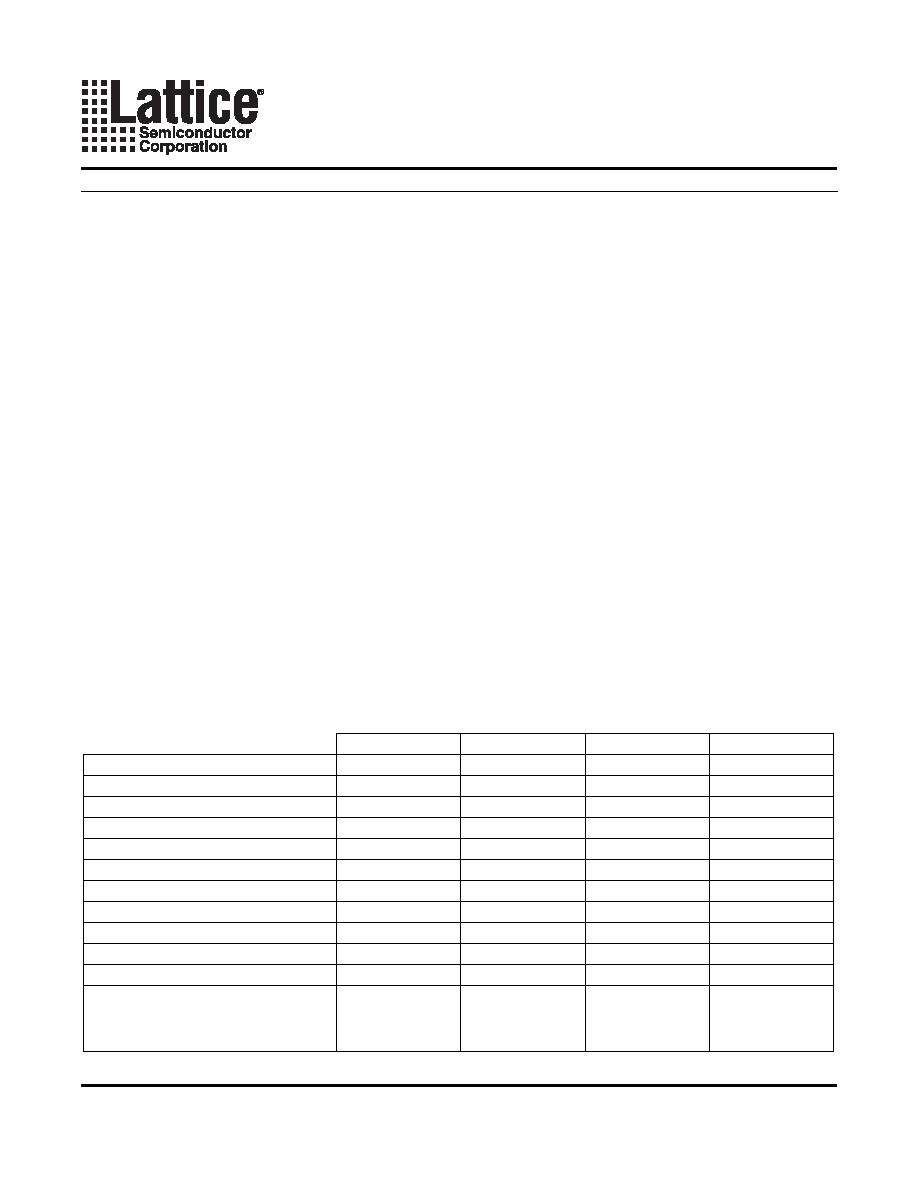
Table 1. ispXPLD 5000MX Family Selection Guide
Note: ispXPLD 5256MX/5512MX/51024MX information is preliminary. ispXPLD 5768MX information is advance.
ispXPLD 5256MX
ispXPLD 5512MX
ispXPLD 5768MX ispXPLD 51024MX
Macrocells
256
512
768
1,024
Multi-Function Blocks
8
16
24
32
Maximum RAM Bits
128K
256K
384K
512K
Maximum CAM Bits
48K
96K
144K
192K
sysCLOCK PLLs
2
2
2
2
t
PD
(Propagation Delay)
4.0ns
4.5ns
5.0ns
5.2ns
t
S
(Register Set-up Time)
2.2ns
2.9ns
3.0ns
3.0ns
t
CO
(Register Clock to Out Time)
2.8ns
3.0ns
3.8ns
3.8ns
f
MAX
(Maximum Operating Frequency)
300MHz
250MHz
240MHz
235MHz
System Gates
75K
150K
225K
300K
I/Os
141
149/193/253
193/317
317/381
Packages
256 fpBGA
208 PQFP
256 fpBGA
484 fpBGA
256 fpBGA
484 fpBGA
484 fpBGA
672 fpBGA

Lattice Semiconductor
ispXPLD 5000MX Family Data Sheet
2
Figure 1. ispXPLD 5000MX Block Diagram
Introduction
The ispXPLD 5000MX family represents a new class of device, referred to as the eXpanded Programmable Logic
Devices (XPLDs). These devices extend the capability of Lattice's popular SuperWIDE ispMACH 5000 architecture
by providing flexible memory capability. The family supports single- or dual-port SRAM, FIFO, and ternary CAM
operation. Extra logic has also been included to allow efficient implementation of arithmetic functions. In addition,
sysCLOCK PLLs and sysIO interfaces provide support for the system-level needs of designers.
The devices provide designers with a convenient one-chip solution that provides logic availability at boot-up, design
security, and extreme reconfigurability. The use of advanced process technology provides industry-leading perfor-
mance with combinatorial propagation delay as low as 4.0ns, 2.8ns clock-to-out delay, 2.2ns set-up time, and oper-
ating frequency up to 300MHz. This performance is coupled with low static and dynamic power consumption. The
ispXPLD 5000MX architecture provides predictable deterministic timing.
The availability of 3.3, 2.5 and 1.8V versions of these devices along with the flexibility of the sysIO interface helps
users meet the challenge of today's mixed voltage designs. Inputs can be safely driven up to 5.5V when an I/O
bank is configured for 3.3V operation, making this family 5V tolerant. Boundary scan testability further eases inte-
gration into today's complex systems. A variety of density and package options increase the likelihood of a good fit
for a particular application. Table 1 shows the members of the ispXPLD 5000MX family.
Architecture
The ispXPLD 5000MX devices consist of Multi-Function Blocks (MFBs) interconnected with a Global Routing Pool.
Signals enter and leave the device via one of four sysIO banks. Figure 1 shows the block diagram of the ispXPLD
ISP Port
Global
Routing
Pool
(GRP)
sysCLOCK
PLL 0
sysCLOCK
PLL 1
sysIO
Bank 0
MFB
MFB
MFB
MFB
V
CCO3
V
CC
V
REF3
V
REF2
V
CCO2
GCLCK3
GCLK2
RESET
GOE0
GOE1
TDO
GND
TDI
TMS
TCK
PROGRAM
OSA
sysIO
Bank 1
sysIO
Bank 3
sysIO
Bank 2
MFB
MFB
MFB
MFB
OSA
OSA
O
SA
V
CCO0
V
CCO1
V
CCP
V
REF0
V
REF1
GCLCK0
GNDP
GCLK1
Optional
sysCONFIG
Interface
V
CCJ

Lattice Semiconductor
ispXPLD 5000MX Family Data Sheet
3
5000MX. Incoming signals may connect to the global routing pool or the registers in the MFBs. An Output Sharing
Array (OSA) increases the number of I/O available to each MFB, allowing a complete function high-performance
access to the I/O. There are four clock pins that drive four global clock nets within the device. Two sysCLOCK PLLs
are provided to allow the synthesis of new clocks and control of clock skews.
Multi-Function Block (MFB)
Each MFB in the ispXPLD 5000MX architecture can be configured in one of the six following modes. This provides
a flexible approach to implementing logic and memory that allows the designer to achieve the mix of functions that
are required for a particular design, maximizing resource utilization. The six modes supported by the MFB are:
� SuperWIDE Logic Mode
� True Dual-port SRAM Mode
� Pseudo Dual-port SRAM Mode
� Single-port SRAM Mode
� FIFO Mode
� Ternary CAM Mode
The MFB consists of a multi-function array and associated routing. Depending on the chosen functions the multi-
function array uses up to 68 inputs from the GRP and the four global clock and reset signals. The array outputs
data along with certain control functions to the macrocells. Output signals can be routed internally for use else-
where in the device and to the sysIO banks for output. Figure 2 shows the block diagram of the MFB. The various
configurations are described in more detail in the following sections.
Figure 2. MFB Block Diagram
To Routing
Reset
CLK0
CLK3
CLK1
CLK2
PTOE
Sharing
To I/O via OSA
Cascade In
Cascade Out
Multifunction Array
True Dual Port
RAM
(8,192 bit)
Pseudo Dual
Port RAM
(16,384 bit)
Single Port
RAM
(16,384 bit)
FIFO
(16,384 bit)
Ternary CAM
(128*48)
Logic
(68 Input * 164 Product
Term Array, 32 MC)
32 Feedback Signals

Lattice Semiconductor
ispXPLD 5000MX Family Data Sheet
4
Cascading For Wide Operation
In several modes it is possible to cascade adjacent MFBs to support wider operation. Table 2 details the different
cascading options. There are chains of MFBs in each device which determine those MFBs that are adjacent for the
purposes of cascading. Table 3 indicates these chains. The ispXPLD 5000MX design tools automatically cascade
blocks if required by a particular design.
Table 2. Cascading Modes For Wide Support
Table 3. MFB Cascade Chain
SuperWIDE Logic Mode
In logic mode, each MFB contains 32 macrocells and a fully populated, programmable AND-array with 160 logic
product terms and four control product terms. The MFB has 68 inputs from the Global Routing Pool, which are
available in both true and complement form for every product term. It is also possible to cascade adjacent MFBs to
create a block with 136 inputs. The four control product terms are used for shared reset, clock, clock enable, and
output enable functions. Figure 3 shows the overall structure of the MFB in logic mode while Figure 4 provides a
more detailed view from the perspective of a macrocell slice.
Mode
Cascading Function
Logic
Input Width.
Allows two MFBs to act as a 136-input block.
Arithmetic.
Allow the carry chain to pass between two MFBs.
FIFO
Memory Width Expansion.
Allows MFBs to be cascaded for greater width support.
CAM
Memory Width Expansion.
Allows up to four MFBs to be cascaded for greater width support.
Device
MFBs in Cascade Chain
ispXPLD 5256MX
A
B
C
D
E
F
G
H
ispXPLD 5512MX
A
B
C
D
E
F
G
H
P
N
M
L
K
J
I
ispXPLD 5768MX
D
C
B
A
X
W
V
U
T
S
R
Q
E
F
G
H
I
J
K
L
M
N
O
P
ispXPLD 51024MX
H
G
F
E
D
C
B
A
AF
AE
AD
AC
AB
AA
Z
Y
I
J
K
L
M
N
O
P
Q
R
S
T
U
V
W
X

Lattice Semiconductor
ispXPLD 5000MX Family Data Sheet
5
Figure 3. MFB in SuperWIDE Logic Mode
Figure 4. Macrocell Slice in Logic Mode AND-Array
To Routing
Reset
CLK0
CLK3
CLK1
CLK2
PTOE
Sharing
To I/O via OSA
Carry In
Carry Out
68 Inputs
from
Routing
68 Inputs*
from
Adjacent
MFB
*Note: These inputs are used for width expansion when more
inputs are needed for CPLD or Memory mode. Single MFB consists
of 68 inputs.
AND Array
68 inputs 164 P-Term
Dual-OR Gate
PT Sharing Array
Shared PT Reset
Shared PT Clk
32 Macrocells
32 Macrocell Feedback Signals
Shared PT Clk En
From
GRP
68
PTSA
From
n-7
Carry-in
To
n+7
PTSA Bypass
PT OE to
I/O Block
From
I/O Cell
PT Clock
PT Preset
PT Reset
Shared PT Reset
Shared
PT CE
CLK0
Shared PTCLK
CLK1
CLK2
CLK3
Global Reset
Clk En
Clk
R/L
D
P
R
Q
AND Array
Dual-OR Array
Macrocell
Output
to I/O Block
GRP
Carry-out