
www.latticesemi.com
1
5kb_011
ispMACH
5000B Family
2.5V In-System Programmable
SuperWIDE
High Density PLDs
September 2002
Data Sheet
Table 1. ispMACH 5000B Family Selection Guide
ispMACH
5128B
ispMACH
5256B
ispMACH
5384B
ispMACH
5512B
Macrocells
128
256
384
512
User I/O Options
92
92/144
156/186
156/196/256
t
PD
(ns)
3.0
4.0
4.0
4.5
t
S
≠ Set-up with 0 Hold (ns)
1.7
2.1
2.1
2.5
t
CO
(ns)
2.2
2.7
2.7
2.8
f
MAX
(MHz)
275
250
250
200
Supply Voltage (V)
2.5
2.5
2.5
2.5
Package
128-pin TQFP
128-pin TQFP
208-pin PQFP
256-ball fpBGA
208-pin PQFP
256-ball fpBGA
208-pin PQFP
256-ball fpBGA
484-ball fpBGA
TM
TM
Features
High Speed Logic Implementation
∑ SuperWIDE 68-input logic block
∑ Up to 35 product terms per output
∑ Single-level Global Routing Pool (GRP)
sysIO
TM
Capability
∑ LVCMOS 1.8, 2.5 and 3.3
∑ LVTTL
∑ SSTL 2 (I and II)
∑ SSTL 3 (I and II)
∑ CTT 3.3, CTT 2.5
∑ HSTL (I and III)
∑ PCI 3.3
∑ GTL+
∑ AGP-1X
∑ LVDS (clock input)
∑ LVPECL (clock input)
∑ Programmable drive strength
Ease of Design
∑ Product term sharing
∑ Extensive clocking and OE capability
Broad Device Offering
∑ 128 to 512 macrocells
∑ 92 to 256 I/Os
∑ 128 to 484 pins/balls in TQFP, PQFP and fpBGA
packages
∑ Commercial and industrial temperature ranges
Easy System Integration
∑ 2.5V power supply
∑ Hot socketing
∑ Input pull-up, pull-down or Bus-keeper
(Pin-by-pin selectable)
∑ Open drain capability
∑ Macrocell-based power management
∑ IEEE 1149.1 Boundary Scan testable
∑ IEEE 1532 compliant In-System Programmable
(ISPTM)
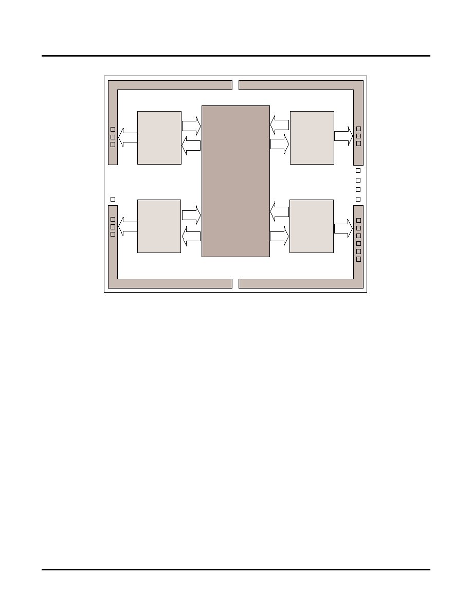
ispMACH 5000B Introduction
The ispMACH 5000B represents the next generation of
Lattice's SuperWIDE CPLD architecture. Through their
wide 68-input blocks, these devices give significantly
improved speed performance for typical designs over
architectures with a lower number of inputs.
In addition to the unique benefits of the SuperWIDE
architecture, the ispMACH 5000B provides sysIO capa-
bility to provide support for a variety of advanced I/O
standards.
The ispMACH 5000B devices consist of multiple Super-
WIDE 68-input, 32-macrocell Generic Logic Blocks
(GLBs) interconnected by a single-level routing system
referred to as the Global Routing Pool (GRP). Figure 1
shows the ispMACH 5000B block diagram. Together,
the GLBs and the GRP allow designers to create large
designs in a single device without compromising perfor-
mance.
Lattice Semiconductor
ispMACH 5000B Family Data Sheet
2
Figure 1. Functional Block Diagram
The GLB has 68 inputs coming from the GRP and contains 163 product terms. These product terms form groups of five
product term clusters, which feed the product term sharing array and the macrocell directly. The ispMACH 5000B allows
up to 35 product terms to be connected to a single macrocell via the Product Term Sharing Array. The macrocell is
designed to provide flexible clocking and control functionality with the capability to select between global, product
term, and block-level resources. The outputs of the macrocells are fed back into the switch matrices and, if
required, the sysIO cell.
All I/Os in the ispMACH 5000B family are sysIO capable, which are split into four banks. Each bank has a separate
I/O power supply and reference voltage. The sysIO cells allow operation with a wide range of today's emerging
interface standards. Within a bank, inputs can be set to a variety of standards providing the reference voltage
requirements of the chosen standards are compatible. Within each bank, the outputs can be set to differing stan-
dards providing the I/O power supply requirements of the chosen standard are compatible. Support for this wide
range of standards allows designers to achieve significantly higher board-level performance compared to the more
traditional LVCMOS standards. Table 1 shows the key attributes and packages for the ispMACH5000B devices.
ispMACH 5000B Architecture
The ispMACH 5000B Family of In-System Programmable (ISPTM) high density programmable logic devices is
based on Generic Logic Blocks (GLBs) and a global routing pool (GRP) structure interconnecting the GLBs.
Outputs from the GLBs drive the GRP. Enhanced switching resources are provided to allow signals in the GRP to
drive any or all of the GLBs. This mechanism allows fast, efficient connections across the entire device. Figure 1
shows the basic ispMACH 5000B architecture.
Generic Logic Block
Each GLB contains 32 macrocells and a fully populated, programmable AND-array with 160 logic product terms
and three GLB-level control product terms. The GLB has 68 inputs from the GRP, which are available in both true
and complement form for every product term. The three control product terms are used for shared reset, clock and
output enable functions.
I/O Bank 0
Global Routing Pool
I/O Bank 3
I/O Bank 1
I/O Bank 2
GCLK0
GCLK1
TOE
VCCO0
TDO
TMS
TCK
TDI
VREF0
VCCO1
VREF1
GCLK3
GCLK2
VCCO3
VREF3
VCCO2
VREF2
RESETB
GOE1
GOE2
Generic
Logic
Block
Generic
Logic
Block
Generic
Logic
Block
Generic
Logic
Block
Lattice Semiconductor
ispMACH 5000B Family Data Sheet
3
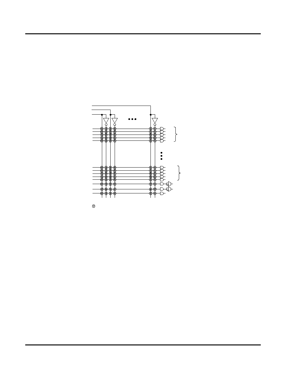
AND-Array
The programmable AND-array consists of 68 inputs and 163 output product terms. The 68 inputs from the GRP are
used to form 136 lines in the AND-array (true and complement of the inputs). Each line in the array can be con-
nected to any of the 163 output product terms via a wired AND. Each of the 160 logic product terms feed the Dual-
OR Array with the remaining three control product terms feeding the Shared PT Clock, Shared PT Reset, and
Shared PT OE. Every set of five product terms from the 160 logic product terms forms a product term cluster start-
ing with PT0. There is one product term cluster for every macrocell in the GLB. In addition to the three control prod-
uct terms, the first, third, fourth and fifth product terms of each cluster can be used as a PTOE (output macrocells
only), PT Clock, PT Preset and PT Reset, respectively. Figure 2 is a graphical representation of the AND-Array.
Figure 2. ispMACH 5000B AND-Array
Dual-OR Array
There are two OR gates per macrocell in the GLB. These OR gates are referred to as the PTSA OR gate and the
PTSA-Bypass OR gate. The PTSA-Bypass OR gate receives its five inputs from the combination of product terms
associated with the product term cluster. The PTSA-Bypass OR gate feeds the macrocell directly for fast narrow
logic. The PTSA OR gate receives its inputs from the combination of product terms associated with the product
term cluster. Figure 3 shows the Dual-OR Array.
PT0
PT1
Cluster 0
PT2
PT3
PT4
In[0]
In[66]
In[67]
Note:
Indicates programmable fuse.
PT160
PT161
PT162
Shared clock
Shared reset
Shared OE
PT156
PT157
PT158
PT159
PT155
Cluster 31

Lattice Semiconductor
ispMACH 5000B Family Data Sheet
4
Figure 3. ispMACH 5000B Dual-OR Array
Product Term Sharing Array
The Product Term Sharing Array (PTSA) consists of 32 inputs from the Dual-OR Array and 32 outputs directly to
the macrocells. Each output is the OR term of any combination of the seven PTSA OR terms connected to that out-
put. Every Nth macrocell is connected to N-3, N-2, N-1, N, N+1, N+2, and N+3 PTSA OR terms via a programma-
ble connection. Figure 4 shows the graphical representation of the PTSA.
Figure 4. ispMACH 5000B PTSA
From PT0
From PT1
From PT2
From PT3
From PT4
PTSA Bypass
To Macrocell
To I/O Block
To Macrocell
To Macrocell
To Macrocell
To PTSA
PT OE
PT Clock
PT Preset
PT Reset
n
PTSA OR 0
PTSA OR 1
PTSA OR 2
PTSA OR 3
PTSA OR 29
PTSA OR 30
PTSA OR 31
Macrocell 0
Macrocell 1
Macrocell 2
Macrocell 29
Macrocell 30
Macrocell 31

Lattice Semiconductor
ispMACH 5000B Family Data Sheet
5
Macrocell
The 32 registered macrocells in the GLB are driven by the 32 outputs from the PTSA or the PTSA bypass. Each
macrocell contains a programmable XOR gate, a programmable register/latch flip-flop and the necessary clocks
and control logic to allow combinatorial or registered operation.
The macrocells each have two outputs, which can be fed to the GRP and I/O cell. This dual or concurrent output
capability from the macrocell gives efficient use of the hardware resources. One output can be a registered function
for example, while the other output can be an unrelated combinatorial function. A direct register input from the I/O
cell facilitates efficient use of the macrocell to construct high-speed input registers.
Macrocell registers can be clocked from one of several global or product term clocks available on the device. A glo-
bal and product term clock enable is also provided, eliminating the need to gate the clock to the macrocell registers
directly. Reset and preset for the macrocell register is provided from both global and product term signals. The
macrocell register can be programmed to operate as a D-type register or a D-type latch. Figure 5 is a graphical rep-
resentation of the ispMACH 5000B macrocell.
Figure 5. ispMACH 5000B Macrocell
I/O Cell
The ispMACH 5000B I/O cell provides a high degree of flexibility. It includes the sysIO feature and an enhanced
output enable MUX for optimal performance both on- and off-chip. The sysIO feature allows I/O cells to be config-
ured to different I/O standards, drive strengths and slew rates. The enhanced output enable MUX provides up to 14
different output enable choices per I/O cell.
The I/O cell contains an output enable (OE) MUX, a programmable tri-state output buffer, a programmable input
buffer, a programmable pull-up resistor, a programmable pull-down resistor and a programmable bus-friendly latch.
The I/O cell receives its input from its associated macrocell. The I/O cell has a feedback line to its associated mac-
rocell and a direct path to the GRP.
The output enable (OE) MUX selects the OE signal per I/O cell. The inputs to the OE MUX are the four shared
PTOE signals, PTOE, the two GOE signals. The OE MUX also has the ability to choose either the true or inverse of
From
GRP
68
Speed/
Power
PTSA
PTSA Bypass
PT OE to
I/O Block
From
I/O Cell
PT Clock
PT Preset
PT Reset
Shared PT Reset
Shared PT Clock
CLK0
CLK1
CLK2
CLK3
Global Reset
Clk En
Clk
R/L
D
P
R
Q
AND Array
Dual-OR Array
Macrocell
Output
to I/O Block
GRP

Lattice Semiconductor
ispMACH 5000B Family Data Sheet
6
each of these signals. The output of the OE MUX goes through a logical AND with the TOE signal to allow easy tri-
stating of the outputs for testing purposes.
The four Shared PTOE signals are derived from PT163 of each GLB. The PTOE signal is derived from the first
product term in each macrocell cluster, which is directly routed to the OE MUX. Therefore, every I/O cell can have a
different OE signal. Figure 6 is a graphical representation of the I/O cell.
Figure 6. ispMACH 5000B I/O Cell
sysIO Capability
The ispMACH 5000B devices are divided into four sysIO banks, where each bank is capable of supporting 14 dif-
ferent I/O standards. Each sysIO bank has its own I/O supply voltage (V
CCO
), reference voltage (V
REF
), and termi-
nation voltage (V
TT
, as applicable), resources allowing each bank complete independence from the others. Each
I/O within a bank is individually configurable consistent with the V
CCO
and V
REF
settings. In addition, each I/O has
individually configurable drive strength, weak pull-up, weak pull-down or a bus-friendly latch. Table 2 lists the
sysIO standards with the typical values for V
CCO
, V
REF
and V
TT
.
The TOE and JTAG pins of the ispMACH 5000B device are the only pins that do not have sysIO capabilities. These
pins support the 2.5V LVTTL and LVCMOS standards.
There are three classes of I/O interface standards implemented in the ispMACH 5000B devices. The first is the
un-terminated, single-ended interface. It includes the 3.3V LVTTL standard along with the 1.8V, 2.5V and 3.3V
LVCMOS interface standards. Additionally, PCI and AGP-1X are all subsets of this type of interface.
The second type of interface implemented is the terminated, single-ended interface standard. This group of inter-
faces includes different versions of SSTL and HSTL interfaces along with CTT, GTL+ and single-ended LVPECL.
Use of these particular I/O interfaces requires an additional V
REF
signal. At the system level a termination voltage,
V
TT
, is also required. Typically an output will be terminated to V
TT
at the receiving end of the transmission line it is
driving.
The final type of interfaces implemented are the differential standards LVDS and LVPECL. These interfaces are
implemented on clock pins only. When using one of the differential standards, a pair of global clock pins (GCLK0
and GCLK1 or GCLK2 and GCLK3) are combined to create a single clock signal.
Global PTOE 0
Global PTOE 1
Global PTOE 2
Global PTOE 3
PTOE
GOE0
GOE1
TOE
V
CCO
to all
other I/Os
in bank
V
CC
for
whole chip
V
REF
to all
other I/Os in bank
V
REF
dependent
Input Buffer
CMOS/TTL
Input Buffer
(V
REF
independent)
I/O
Pad
GND
Output Buffer
(V
CCO
independent for
open drain outputs)
Data Output
from Macrocell
Data Input to Routing
Data Input to Macrocell
+
≠

Lattice Semiconductor
ispMACH 5000B Family Data Sheet
7
For more information on the sysIO capability, please refer to technical note number TN1000,
sysIO Design and
Usage Guidelines
available on the Lattice web site at www.latticesemi.com.
Table 2. ispMACH 5000B Supported I/O Standards
GLB Clock Distribution
The ispLSI 5000B family has four dedicated clock input pins: GCLK0-GCLK3. These feed the Global Clock MUX,
which generates the four global clock signals (CLK0-CLK3). The global clock MUX allows a variety of combinat-
tions of complementary forms of the clock to be used within the device. Additionally, the ispMACH 5000B clock dis-
tribution network offers a differential pair of clock inputs into the global clock MUX for added flexibility. Figure 7
shows the global clock MUX.
The global clock pins are arranged in two pairs, GCLK0 and GCLK1 signals are in one pair and GCLK2 and
GCLK3 signals are in the other pair. The pins are arranged on the die such that each pair of external clock signals
can generate one internal clock from either side of the die when used in differential inputs. This arrangement allows
the clock pins to be used either as four single ended clock signals or two differential (LVPECL or LVDS) clock sig-
nal. Both polarities of the clock are available to drive the internal clock distribution networks.
Figure 7. ispMACH 5000B Global Clock MUX
sysIO Standard
V
CCO
V
REF
V
TT
LVTTL
3.3V
N/A
N/A
LVCMOS 3.3
3.3V
N/A
N/A
LVCMOS 2.5
2.5V
N/A
N/A
LVCMOS 1.8
1.8V
N/A
N/A
PCI 3.3
3.3V
N/A
N/A
AGP-1X
3.3V
N/A
N/A
SSTL3, Class I, II
3.3V
1.5V
1.5V
SSTL2, Class I, II
2.5V
1.25V
1.25V
CTT 3.3
3.3V
1.5V
1.5V
CTT 2.5
2.5V
1.25V
1.25V
HSTL, Class I
1.5V
0.75V
0.75V
HSTL, Class III
1.5V
0.9
0.75V
GTL+
N/A
1.0V
1.5V
VREF0
GCLK0
GCLK1
GCLK3
GCLK2
CLK0
CLK1
CLK2
CLK3
VREF1
VREF3
VREF2
+
≠
+
≠
+
≠
+
≠

Lattice Semiconductor
ispMACH 5000B Family Data Sheet
8
Power Management
The ispMACH 5000B devices provide unique power management controls. The device has two power settings,
high power and low power, on a per node basis. Low power consumption is approximately 50% of high power con-
sumption with a timing delay adder (t
LP
) to the routing delay of the low power node. Each node can be configured
as either high power or low power. However, care should be taken when sharing product terms between nodes with
different power settings.
The ispMACH 5000B devices also have a power-off feature for product terms that are not used. By default, any product
term that is not used is configured as such. This allows the device to operate at minimal power consumption without
affecting the timing of the design. For further information on power management, please refer to technical note number
TN1023,
Power Estimation in ispMACH 5000B Devices
available on the Lattice web site at www.latticesemi.com.
IEEE 1149.1-Compliant Boundary Scan Testability
All ispMACH 5000B devices have boundary scan cells and are compliant to the IEEE 1149.1 standard. This allows
functional testing of the circuit board on which the device is mounted through a serial scan path that can access all
critical logic nodes. Internal registers are linked internally, allowing test data to be shifted in and loaded directly
onto test nodes, or test node data to be captured and shifted out for verification. In addition, these devices can be
linked into a board-level serial scan path for more board-level testing.
sysIO Quick Configuration
To facilitate the most efficient board test, the physical circuit configuration of the I/O cells must be set before run-
ning any continuity tests. As these tests are fast, by nature, the overhead and time that is required for configuration
of the I/Os should be minimal so that board test time is minimized. The ispMACH 5000B family of devices supports
this by offering the user the ability to quickly configure the I/O standard supported by the sysIO cells. This quick
configuration takes milliseconds to complete, whereas it takes seconds for the entire device to be programmed.
Lattice's ispVMTM System programming software can either perform the quick configuration through the PC parallel
port, or can generate the ATE or test vectors necessary for a third-party test system.
IEEE 1532-Compliant In-System Programming
In-system programming of devices provides a number of significant benefits including rapid prototyping, lower inven-
tory levels, higher quality, and the ability to make in-field modifications. All ispMACH 5000B devices provide in-system
programmability through their Boundary Scan Test Access Port. This capability has been implemented in a manner
that ensures that the port remains compliant to the IEEE 1532 standard. By using IEEE 1532 as the communication
interface through which ISP is achieved, customers get the benefit of a standard, well-defined interface.
The ispMACH 5000B devices can be programmed across the commercial temperature and voltage range. The PC-
based Lattice software facilitates in-system programming of ispMACH 5000B devices. The software takes the
JEDEC file output produced by the design implementation software, along with information about the JTAG chain,
and creates a set of vectors that are used to drive the JTAG chain. The software can use these vectors to drive a
JTAG chain via the parallel port of a PC. Alternatively, the software can output files in formats understood by com-
mon automated test equipment. This equipment can then be used to program ispMACH 5000B devices during the
testing of a circuit board.
Security Scheme
A programmable security scheme is provided on the ispMACH 5000B devices as a deterrent to unauthorized copy-
ing of the array configuration patterns. Once programmed, this security prevents readback of the programmed pat-
tern by a device programmer, securing proprietary designs from competitors. The security scheme also prevents
programming and verification. The entire device must be erased in order to reset the security scheme.
Hot Socketing
The ispMACH 5000B devices are well suited for those applications that require hot socketing capability. Hot socket-
ing a device requires that the device, when powered down, can tolerate active signals on the I/Os and inputs with-

Lattice Semiconductor
ispMACH 5000B Family Data Sheet
9
out being damaged. Additionally, it requires that the effects of the powered-down device be minimal on active
signals.
Density Migration
The ispMACH 5000B family has been designed to ensure that different density devices in the same package have
the same pin-out. Furthermore, the architecture ensures a high success rate when performing design migration
from lower density parts to higher density parts. In many cases, it is possible to shift a lower utilization design tar-
geted for a high density device to a lower density device. However, the exact details of the final resource utilization
will impact the likely success in each case.

Lattice Semiconductor
ispMACH 5000B Family Data Sheet
10
Absolute Maximum Ratings
1, 2, 3
Supply Voltage V
CC
. . . . . . . . . . . . . . . . . . . . . . . . . -0.5 to 4.05V
Output Supply Voltage V
CCO
. . . . . . . . . . . . . . . . . . -0.5 to 4.05V
Input Voltage Applied
4
. . . . . . . . . . . . . . . . . . . . . . . -0.5 to 4.05V
Tri-state Output Voltage Applied. . . . . . . . . . . . . . . . -0.5 to 4.05V
Storage Temperature . . . . . . . . . . . . . . . . . . . . . . . . -65 to 150
∞
C
Junction Temperature (Tj) with Power Applied . . . . . -55 to 130
∞
C
1. Stress above those listed under the "Absolute Maximum Ratings" may cause permanent damage to the device. Functional
operation of the device at these or any other conditions above those indicated in the operational sections of this specification
is not implied.
2. Compliance with Lattice
Thermal Management
document is required.
3. All voltages referenced to GND.
4. Overshoot and Undershoot of -2V to (V
IHMAX
+2) volts is permitted for a duration of < 20ns.
Recommended Operating Conditions
Erase Reprogram Specifications
Hot Socketing Characteristics
1,2,3
Symbol
Parameter
Min
Max
Units
V
CC
Supply Voltage
2.3
2.7
V
T
J
Junction Temperature (Commercial)
0
90
C
Junction Temperature (Industrial)
-40
105
C
Parameter
Min
Max
Units
Erase/Reprogram Cycle
1,000
--
Cycles
Symbol
Parameter
Condition
Min
Typ
Max
Units
I
DK
Input or I/O Leakage Current
0
V
IN
V
IH
(MAX)
--
--
+/- 100
µ
A
V
IH
(MAX)
V
IN
3.6V
--
--
+/- 100
µ
A
1. Insensitive to sequence of V
CC
and V
CCO
. However, assumes monotonic rise / fall rates for V
CC
and V
CCO
.
2. LVTTL, LVCMOS only
3. 0
V
CC
V
CC
(MAX), 0
V
CCO
V
CCO
(MAX)

Lattice Semiconductor
ispMACH 5000B Family Data Sheet
11
DC Electrical Characteristics
Over Recommended Operating Conditions
Supply Current
Symbol
Parameter
Condition
Min
Typ
Max
Units
I
IL
, I
IH
1, 2
Input 0V
V
IN
V
CC
--
--
+/- 10
µ
A
I/O
0V
V
IN
V
CCO
--
--
+/- 10
µ
A
I
DK
Input V
CC
V
IN
3.6V
--
--
+/- 100
µ
A
I/O
V
CCO
V
IN
3.6V
--
--
+/- 100
µ
A
I
PU
2
I/O Weak Pull-up Resistor Current
0V
V
IN
1.7V
-30
--
-150
µ
A
1.7V < V
IN
2.0V
-15
--
-150
µ
A
I
PD
2
I/O Weak Pull-down Resistor Current V
IL
(MAX)
V
IN
V
IH
(MAX)
30
--
150
µA
I
BHLS
2
Bus Hold Low Sustaining Current
V
IN
= V
IL
(MAX)
30
--
--
µA
I
BHHS
2
Bus Hold High Sustaining Current
V
IN
= 1.7V
-30
--
--
µA
V
IN
= 2.0V
-15
--
--
µA
I
BHLO
2
Bus Hold Low Overdrive Current
0V V
IN
3.6V
--
--
150
µA
I
BHHO
2
Bus Hold High Overdrive Current
0V V
IN
3.6V
--
--
-150
µA
V
BHT
Bus Hold Trip Points
V
IL
(MAX)
--
V
IH
(MIN)
V
I
CCO
3, 4, 5, 6
I/O Supply Current
No Output Loading
V
CCO
= 3.3V
--
--
10
mA
No Output Loading
V
CCO
= 2.5V
--
--
10
mA
No Output Loading
V
CCO
= 1.8V
--
--
10
mA
C
1
I/O Capacitance
3
V
CC
= 2.5V, V
IO
= 0 to 3.6V
--
8
--
pf
C
2
Clock Capacitance
3
V
CC
= 2.5V, V
CLOCK
= 0 to 3.6V
--
10
--
pf
C
3
Global Input Capacitance
3
V
CC
= 2.5V, V
GLOBAL
= 0 to 3.6V
--
10
--
pf
1. Input or I/O leakage current is measured with the pin configured as an input or as an I/O with the output driver tri-stated. It is not
measured with the output driver active. Bus maintenance circuits are disabled.
2. Only available for LVCMOS and LVTTL standards.
3. T
A
= 25∞C, f = 1.0MHz.
4. Device configured with 16-bit counters.
5. I
CC
varies with specific device configuration and operating frequency.
6. Per bank.
Symbol
Parameter
Condition
Min
Typ
Max
Units
ispMACH 5128B
I
CC
1, 2, 3
Operating Power Supply Current
V
CCO
= 2.5V
--
83
--
mA
ispMACH 5256B
I
CC
1, 2, 3
Operating Power Supply Current
V
CCO
= 2.5V
--
130
--
mA
ispMACH 5384B
I
CC
1, 2, 3
Operating Power Supply Current
V
CCO
= 2.5V
--
216
--
mA
ispMACH 5512B
I
CC
1, 2, 3
Operating Power Supply Current
V
CCO
= 2.5V
--
270
--
mA
1. T
A
= 25∞C, f = 1.0MHz.
2. Device configured with 16-bit counters.
3. I
CC
varies with specific device configuration and operating frequency.

Lattice Semiconductor
ispMACH 5000B Family Data Sheet
12
sysIO Recommended Operating Conditions
Standard
V
CCO
(V)
V
REF
(V)
Min
Max
Min
Max
LVTTL
3.0
3.6
--
--
LVCMOS 3.3
3.0
3.6
--
--
LVCMOS 2.5
1
2.3
2.7
--
--
LVCMOS 1.8
1.65
1.95
--
--
PCI 3.3
3.0
3.6
--
--
AGP-1X
3.15
3.45
--
--
SSTL 3, Class I, II
3.0
3.6
1.3
1.7
SSTL 2, Class I, II
2.3
2.7
1.15
1.35
CTT 3.3
3.0
3.6
1.35
1.65
CTT 2.5
2.3
2.7
1.35
1.65
HSTL
1.4
1.6
0.68
0.9
GTL+
1.4
3.6
0.882
1.122
1. Software default setting.

Lattice Semiconductor
ispMACH 5000B Family Data Sheet
13
sysIO DC Electrical Characteristics
Over Recommended Operating Conditions
sysIO Differential Input DC Electrical Characteristics and Operating Conditions
Input/Output
Standard
V
IL
V
IH
V
OL
Max (V)
V
OH
Min (V)
I
OL
2
(mA)
I
OH
2
(mA)
Min (V)
Max (V)
Min (V)
Max (V)
LVCMOS 3.3
-0.3
0.8
2.0
3.6
0.4
2.4
20, 16,
12, 8,
5.33, 4
-20, -16,
-12, -8,
-5.33 -4
LVTTL
-0.3
0.8
2.0
3.6
0.4
2.4
20
20
0.2
V
CCO
- 0.2
0.1
0.1
LVCMOS 2.5
1
-0.3
0.7
1.7
3.6
0.4
V
CCO
- 0.4
8
-8
LVCMOS 2.5
-0.3
0.7
1.7
3.6
0.4
V
CCO
- 0.4
16, 12,
5.33, 4
-16, -12,
-5.33, -4
0.2
V
CCO
- 0.2
0.1
-0.1
LVCMOS 1.8
-0.3
0.68
1.07
3.6
0.4
V
CCO
-0.4
12, 8,
5.33, 4
-12, -8,
-5.33, -4
0.2
V
CCO
- 0.2
0.1
-0.1
PCI 3.3
-0.3
1.08
1.5
3.6
0.1V
CCO
0.9V
CCO
1.5
-0.5
AGP-1X
-0.3
1.08
1.5
3.6
0.1V
CCO
0.9V
CCO
1.5
-0.5
SSTL3 class I
-0.3
V
REF
-0.2
V
REF
+0.2
3.6
0.7
V
CCO
- 1.1
8
-8
SSTL3 class II
-0.3
V
REF
-0.2
V
REF
+0.2
3.6
0.5
V
CCO
- 0.9
16
-16
SSTL2 class I
-0.3
V
REF
-0.18
V
REF
+0.18
3.6
0.54
V
CCO
- 0.62
7.6
-7.6
SSTL2 class II
-0.3
V
REF
-0.18
V
REF
+0.18
3.6
0.35
V
CCO
- 0.43
15.2
-15.2
CTT 3.3
-0.3
V
REF
-0.2
V
REF
+0.2
3.6
V
REF
-0.4
V
REF
+ 0.4
8
-8
CTT 2.5
-0.3
V
REF
-0.2
V
REF
+0.2
3.6
V
REF
-0.4
V
REF
+ 0.4
8
-8
HSTL class I
-0.3
V
REF
-0.1
V
REF
+0.1
3.6
0.4
V
CCO
- 0.4
8
-8
HSTL class III
-0.3
V
REF
-0.1
V
REF
+0.1
3.6
0.4
V
CCO
- 0.4
24
-8
GLT+
-0.3
V
REF
-0.2
V
REF
+0.2
3.6
0.6
N/A
36
N/A
1. Software default setting
2. The average DC current drawn by I/Os between adjacent bank GND connections, or between the last GND in an I/O bank and the end of the
I/O bank, as shown in the logic signals connection table, shall not exceed 96mA.
Symbol Parameter
Test
Conditions
Min
Max
V
INP
. V
INM
LVDS Input voltage
--
0V
2.4V
V
THD
LVDS Differential input
threshold
--
+/- 100mV
--
V
IL
1
LVPECL Input Voltage
Low
V
CCIO
= 3.0 to 3.6V
V
CCIO
-1.81V
V
CCIO
-1.48V
V
CCIO
= 3.3V
1.49V
1.83V
V
IH
1
LVPECL Input Voltage
High
V
CCIO
= 3.0 to 3.6V
V
CCIO
-1.17V
V
CCIO
-0.88V
V
CCIO
= 3.3V
2.14V
2.42V
1. V
CCIO
is in 3.3V range.

Lattice Semiconductor
ispMACH 5000B Family Data Sheet
14
ispMACH 5128B External Switching Characteristics
Over Recommended Operating Conditions
Parameter
Description
1, 2, 3
-3
-5
-75
-10
Units
Min.
Max.
Min.
Max.
Min.
Max.
Min.
Max.
t
PD
Data propagation delay, 5-PT bypass
-
3.0
-
5.0
-
7.5
-
10.0
ns
t
PD_PTSA
Propagation delay
-
3.8
-
6.5
-
9.0
-
12.0
ns
t
S
GLB register setup time before clock, 5-PT
bypass
1.7
-
3.0
-
5.0
-
6.5
-
ns
t
S_PTSA
GLB register setup time before clock
2.2
-
4.0
-
6.5
-
8.5
-
ns
t
SIR
GLB register setup time before clock, input reg-
ister path, 5-PT bypass
2.0
-
2.5
-
3.5
-
5.0
-
ns
t
H
GLB register hold time before clock, 5-PT
bypass
0.0
-
0.0
-
0.0
-
0.0
-
ns
t
H_PTSA
GLB register hold time before clock
0.0
-
0.0
-
0.0
-
0.0
-
ns
t
HIR
GLB register hold time before clock, input
reg.path
0.0
-
0.0
-
0.0
-
0.0
-
ns
t
CO
GLB register clock-to-output delay
-
2.2
-
3.0
-
4.0
-
5.5
ns
t
R
External reset pin to output delay
-
2.5
-
5.0
-
7.5
-
10.0
ns
t
RW
Reset pulse duration
3.0
-
3.5
-
5.0
-
6.5
-
ns
t
PTEN/DIS
Input to output local product term output
enable/disable
-
4.0
-
6.0
-
8.5
-
10.0
ns
t
GPTEN/DIS
Input to output global product term output
enable/disable
-
4.2
-
7.0
-
10.0
-
12.0
ns
t
GOE/DIS
Global OE input to output enable/disable
-
2.5
-
3.7
-
5.5
-
7.5
ns
t
CW
Clock pulse duration
1.3
-
2.2
-
2.5
-
2.8
-
ns
t
GW
Global gate width low (for low transparent) or
high (for high transparent)
1.3
-
2.2
-
2.5
-
2.8
-
ns
t
WIR
Input register clock width, high or low
1.3
-
2.2
-
2.5
-
2.8
-
ns
f
MAX
4
Clock frequency with internal feedback
275
-
180
-
150
-
110
-
MHz
f
MAX
(Ext.)
Clock frequency with external feedback,
1/(t
S_PTSA
+ t
CO
)
227
-
142
-
95
-
71
-
MHz
f
MAX
(Tog.) Clock frequency max toggle
350
-
225
-
200
-
175
-
MHz
Timing v.1.0
1. Timing Numbers are based on default LVCMOS 2.5V, 8mA I/O buffers. Use timing adjusters provided to calculate timing for other stan-
dards.
2. Measured using standard switching circuit, assuming global routing loading of 1, worst case PTSA loading, CLK0, 1 output switching and
high speed AND array.
3. Pulse widths and clock widths less than minimum will cause unknown behavior.
4. Standard 16-bit counter using GRP feedback.

Lattice Semiconductor
ispMACH 5000B Family Data Sheet
15
ispMACH 5256B External Switching Characteristics
Over Recommended Operating Conditions
Parameter
Description
1, 2, 3
-4
-5
-75
-10
Units
Min.
Max.
Min.
Max.
Min.
Max.
Min.
Max.
t
PD
Data propagation delay, 5-PT bypass
-
4.0
-
5.0
-
7.5
-
10.0
ns
t
PD_PTSA
Propagation delay
-
4.8
-
6.5
-
9.0
-
12.0
ns
t
S
GLB register setup time before clock, 5-PT
bypass
2.1
-
3.0
-
5.0
-
6.5
-
ns
t
S_PTSA
GLB register setup time before clock
2.7
-
4.0
-
6.5
-
8.5
-
ns
t
SIR
GLB register setup time before clock, input reg-
ister path, 5-PT bypass
1.9
-
2.5
-
3.5
-
5.0
-
ns
t
H
GLB register hold time before clock, 5-PT
bypass
0.0
-
0.0
-
0.0
-
0.0
-
ns
t
H_PTSA
GLB register hold time before clock
0.0
-
0.0
-
0.0
-
0.0
-
ns
t
HIR
GLB register hold time before clock, input
reg.path
0.0
-
0.0
-
0.0
-
0.0
-
ns
t
CO
GLB register clock-to-output delay
-
2.7
-
3.0
-
4.0
-
5.5
ns
t
R
External reset pin to output delay
-
3.8
-
5.0
-
7.5
-
10.0
ns
t
RW
Reset pulse duration
3.0
-
3.5
5.0
-
6.5
-
ns
t
PTEN/DIS
Input to output local product term output
enable/disable
-
5.0
-
6.0
-
8.5
-
10.0
ns
t
GPTEN/DIS
Input to output global product term output
enable/disable
-
5.5
-
7.0
-
10.0
-
12.0
ns
t
GOE/DIS
Global OE input to output enable/disable
-
3.4
-
3.7
-
5.5
-
7.5
ns
t
CW
Clock pulse duration
1.5
-
2.2
-
2.5
-
2.8
-
ns
t
GW
Global gate width low (for low transparent) or
high (for high transparent)
1.5
-
2.2
-
2.5
-
2.8
-
ns
t
WIR
Input register clock width, high or low
1.5
-
2.2
-
2.5
-
2.8
-
ns
f
MAX
4
Clock frequency with internal feedback
250
-
180
-
150
-
110
-
MHz
f
MAX
(Ext.)
Clock frequency with external feedback,
1/(t
S_PTSA
+ t
CO
)
185
-
142
-
95
-
71
-
MHz
f
MAX
(Tog.) Clock frequency max toggle
333
-
225
-
200
-
175
-
MHz
Timing v.1.3
1. Timing Numbers are based on default LVCMOS 2.5V, 8mA I/O buffers. Use timing adjusters provided to calculate timing for other stan-
dards.
2. Measured using standard switching circuit, assuming global routing loading of 1, worst case PTSA loading, CLK0, 1 output switching and
high speed AND array.
3. Pulse widths and clock widths less than minimum will cause unknown behavior.
4. Standard 16-bit counter using GRP feedback.

Lattice Semiconductor
ispMACH 5000B Family Data Sheet
16
ispMACH 5384B External Switching Characteristics
Over Recommended Operating Conditions
Parameter
Description
1, 2, 3
-4
-5
-75
-10
Units
Min.
Max.
Min.
Max.
Min.
Max.
Min.
Max.
t
PD
Data propagation delay, 5-PT bypass
-
4.0
-
5.0
-
7.5
-
10.0
ns
t
PD_PTSA
Propagation delay
-
4.8
-
6.5
-
9.0
-
12.0
ns
t
S
GLB register setup time before clock, 5-PT
bypass
2.1
-
3.0
-
5.0
-
6.5
-
ns
t
S_PTSA
GLB register setup time before clock
2.7
-
4.0
-
6.5
-
8.5
-
ns
t
SIR
GLB register setup time before clock, input reg-
ister path, 5-PT bypass
1.9
-
2.5
-
3.5
-
5.0
-
ns
t
H
GLB register hold time before clock, 5-PT
bypass
0.0
-
0.0
-
0.0
-
0.0
-
ns
t
H_PTSA
GLB register hold time before clock
0.0
-
0.0
-
0.0
-
0.0
-
ns
t
HIR
GLB register hold time before clock, input
reg.path
0.00
-
0.0
-
0.0
-
0.0
-
ns
t
CO
GLB register clock-to-output delay
-
2.7
-
3.0
-
4.0
-
5.5
ns
t
R
External reset pin to output delay
-
3.8
-
5.0
-
7.5
-
10.0
ns
t
RW
Reset pulse duration
3.0
-
3.5
-
5.0
-
6.5
-
ns
t
PTEN/DIS
Input to output local product term output enable/
disable
-
5.0
-
6.0
-
8.5
-
10.0
ns
t
GPTEN/DIS
Input to output global product term output
enable/disable
-
5.5
-
7.0
-
10.0
-
12.0
ns
t
GOE/DIS
Global OE input to output enable/disable
-
3.4
-
3.7
-
5.5
-
7.5
ns
t
CW
Clock pulse duration
1.5
-
2.2
-
2.5
-
2.8
-
ns
t
GW
Global gate width low (for low transparent) or
high (for high transparent)
1.5
-
2.2
-
2.5
-
2.8
-
ns
t
WIR
Input register clock width, high or low
1.5
-
2.2
-
2.5
-
2.8
-
ns
f
MAX
4
Clock frequency with internal feedback
250
-
180
-
150
-
110
-
MHz
f
MAX
(Ext.)
Clock frequency with external feedback,
1/(t
S_PTSA+tCO
)
185
-
142
-
95
-
71
-
MHz
f
MAX
(Tog.) Clock frequency max toggle
333
-
225
-
200
-
175
-
MHz
Timing v.1.0
1. Timing Numbers are based on default LVCMOS 2.5V, 8mA I/O buffers. Use timing adjusters provided to calculate timing for other standards.
2. Measured using standard switching circuit, assuming global routing loading of 1, worst case PTSA loading, CLK0, 1 output switching and
high speed AND array.
3. Pulse widths and clock widths less than minimum will cause unknown behavior.
4. Standard 16-bit counter using GRP feedback.

Lattice Semiconductor
ispMACH 5000B Family Data Sheet
17
ispMACH 5512B External Switching Characteristics
Over Recommended Operating Conditions
Parameter
Description
1, 2, 3
-45
-75
-10
-12
Units
Min.
Max.
Min.
Max.
Min.
Max.
Min.
Max.
t
PD
Data propagation delay, 5-PT bypass
-
4.5
-
7.5
-
10.0
-
12.0
ns
t
PD_PTSA
Propagation delay
-
5.3
-
9.0
-
12.0
-
15.0
ns
t
S
GLB register setup time before clock, 5-PT
bypass
2.5
-
5.0
-
6.5
-
7.5
-
ns
t
S_PTSA
GLB register setup time before clock
3.1
-
6.5
-
8.5
-
10.5
-
ns
t
SIR
GLB register setup time before clock, input reg-
ister path, 5-PT bypass
1.7
-
3.5
-
5.0
-
5.5
-
ns
t
H
GLB register hold time before clock, 5-PT
bypass
0.0
-
0.0
-
0.0
-
0.0
-
ns
t
H_PTSA
GLB register hold time before clock
0.0
-
0.0
-
0.0
-
0.0
-
ns
t
HIR
GLB register hold time before clock, input
reg.path
0.0
-
0.0
-
0.0
-
0.0
-
ns
t
CO
GLB register clock-to-output delay
-
2.8
-
4.0
-
5.5
-
6.5
ns
t
R
External reset pin to output delay
-
4.2
-
7.5
-
10.0
-
12.0
ns
t
RW
Reset pulse duration
3.0
-
5.0
-
6.5
-
8.0
-
ns
t
PTEN/DIS
Input to output local product term output enable/
disable
-
5.5
-
8.5
-
10.0
-
12.0
ns
t
GPTEN/DIS
Input to output global product term output
enable/disable
-
6.3
-
10.0
-
12.0
-
15.0
ns
t
GOE/DIS
Global OE input to output enable/disable
-
3.5
-
5.5
-
7.5
-
9.0
ns
t
CW
Clock pulse duration
2.0
-
2.5
-
2.8
-
3.3
-
ns
t
GW
Global gate width low (for low transparent) or
high (for high transparent)
2.0
-
2.5
-
2.8
-
3.3
-
ns
t
WIR
Input register clock width, high or low
2.0
-
2.5
-
2.8
-
3.3
-
ns
f
MAX
4
Clock frequency with internal feedback
200
-
150
-
110
-
90
-
MHz
f
MAX
(Ext.) Clock frequency with external feedback,
1/(t
S_PTSA
+ t
CO
)
169
-
95
-
71
-
58
-
MHz
f
MAX
(Tog.) Clock frequency max toggle
250
-
200
-
175
-
150
-
MHz
Timing v.1.1
1. Timing Numbers are based on default LVCMOS 2.5V, 8mA I/O buffers. Use timing adjusters provided to calculate timing for other stan-
dards.
2. Measured using standard switching circuit, assuming global routing loading of 1, worst case PTSA loading, CLK0 and 1 output switching
and high speed AND array.
3. Pulse widths and clock widths less than minimum will cause unknown behavior.
4. Standard 16-bit counter using GRP feedback.

Lattice Semiconductor
ispMACH 5000B Family Data Sheet
18
Timing Model
The task of determining the timing through the ispLSI 5000B family, just as any CPLD, is relatively simple. The tim-
ing model provided in Figure 8 shows the specific delay paths. Once the implementation of a given function is
determined either conceptually or from the design tool report file, the delay path of the function can easily be
derived from the timing model. The design tool reports the timing delays based on the same timing model for a par-
ticular design. Note that the internal timing parameters are given for reference only and are not tested. The external
timing parameters are tested and guaranteed for every device.
Figure 8. ispMACH 5000B Timing Model
t
BLA
t
LP
t
IOI
t
IOI
t
IOI
t
IOI
t
BSR
t
PTSR
t
GPTOE
t
PTOE
t
PDi
t
GOE
t
RST
t
IN
t
INREG
t
ROUTE
t
PDb
t
FBK
t
BUF
t
IOO
t
EN
t
DIS
t
PTSA
t
PTCLK
t
BCLK
t
GCLK_IN
IN
Q
OE
From Feedback
In/Out
Delays
In/Out
Delays
Routing/
GLB Delays
Register/
Latch Delays
Control
Delays
Feedback
OUT
DATA
MC Reg
CE
S/R
CLK
RST
Note: Italicized parameters are delay adders above and beyond default conditions (i.e. GRP load of one GLB, CLK0, high-speed AND Array
and VCC I/O option).

Lattice Semiconductor
ispMACH 5000B Family Data Sheet
19
ispMACH 5128B Internal Timing Parameters
1
Over Recommended Operating Conditions
Parameter
Description
-3
-5
-75
-10
Units
Min.
Max.
Min.
Max.
Min.
Max.
Min.
Max.
In/Out Delays
t
IN
Input Buffer Delay
-
0.30
-
0.60
-
2.00
-
2.40
ns
t
GCLK_IN
Global Clock Input Buffer Delay
-
1.00
-
1.50
-
1.40
-
1.90
ns
t
GOE
Global OE Pin Delay
-
1.60
-
2.60
-
3.00
-
4.40
ns
t
BUF
Delay through Output Buffer
-
0.50
-
0.80
-
1.80
-
2.50
ns
t
EN
Output Enable Time
-
0.90
-
1.10
-
2.50
-
3.10
ns
t
DIS
Output Disable Time
-
0.90
-
1.10
-
2.50
-
3.10
ns
t
RST
Global Rest Pin Delay
-
1.20
-
2.20
-
2.70
-
3.60
ns
Routing Delays
t
ROUTE
Delay through GRP
-
1.60
-
2.50
-
2.60
-
3.70
ns
t
PTSA
Product Term Sharing Array
-
1.10
-
2.10
-
2.60
-
3.40
ns
t
PDb
5-PT Bypass Propogation Delay
-
0.60
-
1.10
-
1.10
-
1.40
ns
t
PDi
Macrocell Propogation Delay
-
0.30
-
0.50
-
0.00
-
0.00
ns
t
INREG
Input Buffer to Macrocell Register Delay
-
2.50
-
3.10
-
2.20
-
3.60
ns
t
FBK
Internal Feedback Delay
-
0.00
-
0.00
-
0.00
-
0.00
ns
Register/Latch Delays
t
S
D-Register Setup Time (Global Clock)
0.20
-
0.30
-
0.70
-
0.90
-
ns
t
S_PT
D-Register Setup Time (Product Term Clock)
0.20
-
0.20
-
0.70
-
0.90
-
ns
t
SL_PT
Latch Setup Time (Product Term Clock)
0.20
-
0.20
-
0.70
-
0.90
-
ns
t
H
D-Register Hold Time
1.50
-
2.70
-
4.30
-
5.60
-
ns
t
COi
Register Clock to Output/Feedback Mux Time
-
0.70
-
0.70
0.80
1.10
ns
t
CES
Clock Enable Setup Time
3.30
-
4.30
-
4.70
-
5.00
-
ns
t
CEH
Clock Enable Hold Time
0.20
-
0.40
-
0.50
-
0.60
-
ns
t
SL
Latch Setup Time
0.20
-
0.30
-
0.70
-
0.90
-
ns
t
HL
Latch Hold Time
1.50
-
2.70
-
4.30
-
5.60
-
ns
t
GOi
Latch Gate to Output/Feedback Mux Time
-
0.70
-
0.60
-
0.80
-
1.60
ns
t
PDLi
Propogation Delay through Transparent Latch
to Output/Feedback Mux
-
0.50
-
0.50
-
0.50
-
0.50
ns
t
SRi
Asynchronous Reset or Set to Output/Feed-
back MUX Delay
-
0.80
-
2.00
-
3.00
-
3.90
ns
t
SRR
Asynchronous Reset or Set Recovery Delay
1.50
-
2.70
-
4.00
-
6.00
-
ns
Control Delays
t
BCLK
GLB PT Clock Delay
-
1.70
-
2.40
-
2.80
-
3.20
ns
t
PTCLK
Macrocell PT Clock Delay
-
1.50
-
2.10
-
2.40
-
2.70
ns
t
BSR
Block PT Set/Reset Delay
-
1.20
-
1.70
-
1.90
-
2.10
ns
t
PTSR
Macrocell PT Set/Reset Delay
-
0.80
-
1.10
-
1.20
-
1.30
ns
t
GPTOE
Global PT OE Delay
-
1.40
-
2.80
-
2.90
-
2.80
ns
t
PTOE
Macrocell PT OE Delay
-
1.20
-
1.80
-
1.40
-
0.80
ns
Timing v.1.0
1. Internal Timing Parameters are not tested and are for reference only. Refer to Timing Model in this data sheet for further details.

Lattice Semiconductor
ispMACH 5000B Family Data Sheet
20
ispMACH 5256B Internal Timing Parameters
1
Over Recommended Operating Conditions
Parameter
Description
-4
-5
-75
-10
Units
Min.
Max.
Min.
Max.
Min.
Max.
Min.
Max.
In/Out Delays
t
IN
Input Buffer Delay
-
0.40
-
0.60
-
2.00
-
2.40
ns
t
GCLK_IN
Global Clock Input Buffer Delay
-
1.20
-
1.50
-
1.40
-
1.90
ns
t
GOE
Global OE Pin Delay
-
2.40
-
2.60
-
3.00
-
4.40
ns
t
BUF
Delay through Output Buffer
-
1.00
-
0.80
-
1.80
-
2.50
ns
t
EN
Output Enable Time
-
1.00
-
1.10
-
2.50
-
3.10
ns
t
DIS
Output Disable Time
-
1.00
-
1.10
-
2.50
-
3.10
ns
t
RST
Global Rest Pin Delay
-
1.30
-
2.20
-
2.70
-
3.60
ns
Routing Delays
t
ROUTE
Delay through GRP
-
1.80
-
2.50
-
2.60
-
3.70
ns
t
PTSA
Product Term Sharing Array
-
1.40
-
2.10
-
2.60
-
3.40
ns
t
PDb
5-PT Bypass Propogation Delay
-
0.80
-
1.10
-
1.10
-
1.40
ns
t
PDi
Macrocell Propogation Delay
-
0.20
-
0.50
-
0.00
-
0.00
ns
t
INREG
Input Buffer to Macrocell Register Delay
-
2.40
-
3.10
-
2.20
-
3.60
ns
t
FBK
Internal Feedback Delay
-
0.00
-
0.00
-
0.00
-
0.00
ns
Register/Latch Delays
t
S
D-Register Setup Time (Global Clock)
0.30
-
0.30
-
0.70
-
0.90
-
ns
t
S_PT
D-Register Setup Time (Product Term Clock)
0.30
-
0.20
-
0.70
-
0.90
-
ns
t
SL_PT
Latch Setup Time (Product Term Clock)
0.30
-
0.20
-
0.70
-
0.90
-
ns
t
H
D-Register Hold Time
1.80
-
2.70
-
4.30
-
5.60
-
ns
t
COi
Register Clock to Output/Feedback Mux Time
-
0.50
-
0.70
0.80
1.10
ns
t
CES
Clock Enable Setup Time
3.90
-
4.30
-
4.70
-
5.00
-
ns
t
CEH
Clock Enable Hold Time
0.30
-
0.40
-
0.50
-
0.60
-
ns
t
SL
Latch Setup Time
0.30
-
0.30
-
0.70
-
0.90
-
ns
t
HL
Latch Hold Time
1.80
-
2.70
-
4.30
-
5.60
-
ns
t
GOi
Latch Gate to Output/Feedback Mux Time
-
0.60
-
0.60
-
0.80
-
1.60
ns
t
PDLi
Propogation Delay through Transparent Latch
to Output/Feedback Mux
-
0.50
-
0.50
-
0.50
-
0.50
ns
t
SRi
Asynchronous Reset or Set to Output/Feed-
back MUX Delay
-
1.50
-
2.00
-
3.00
-
3.90
ns
t
SRR
Asynchronous Reset or Set Recovery Delay
2.00
-
2.70
-
4.00
-
6.00
-
ns
Control Delays
t
BCLK
GLB PT Clock Delay
-
2.00
-
2.40
-
2.80
-
3.20
ns
t
PTCLK
Macrocell PT Clock Delay
-
1.80
-
2.10
-
2.40
-
2.70
ns
t
BSR
Block PT Set/Reset Delay
-
1.50
-
1.70
-
1.90
-
2.10
ns
t
PTSR
Macrocell PT Set/Reset Delay
-
1.00
-
1.10
-
1.20
-
1.30
ns
t
GPTOE
Global PT OE Delay
-
2.30
-
2.80
-
2.90
-
2.80
ns
t
PTOE
Macrocell PT OE Delay
-
1.80
-
1.80
-
1.40
-
0.80
ns
Timing v.1.3
1. Internal Timing Parameters are not tested and are for reference only. Refer to Timing Model in this data sheet for further details.

Lattice Semiconductor
ispMACH 5000B Family Data Sheet
21
ispMACH 5384B Internal Timing Parameters
1
Over Recommended Operating Conditions
Parameter
Description
-4
-5
-75
-10
Units
Min.
Max.
Min.
Max.
Min.
Max.
Min.
Max.
In/Out Delays
t
IN
Input Buffer Delay
-
0.40
-
0.60
-
2.00
-
2.40
ns
t
GCLK_IN
Global Clock Input Buffer Delay
-
1.20
-
1.50
-
1.40
-
1.90
ns
t
GOE
Global OE Pin Delay
-
2.40
-
2.60
-
3.00
-
4.40
ns
t
BUF
Delay through Output Buffer
-
1.00
-
0.80
-
1.80
-
2.50
ns
t
EN
Output Enable Time
-
1.00
-
1.10
-
2.50
-
3.10
ns
t
DIS
Output Disable Time
-
1.00
-
1.10
-
2.50
-
3.10
ns
t
RST
Global Rest Pin Delay
-
1.30
-
2.20
-
2.70
-
3.60
ns
Routing Delays
t
ROUTE
Delay through GRP
-
1.80
-
2.50
-
2.60
-
3.70
ns
t
PTSA
Product Term Sharing Array
-
1.40
-
2.10
-
2.60
-
3.40
ns
t
PDb
5-PT Bypass Propogation Delay
-
0.80
-
1.10
-
1.10
-
1.40
ns
t
PDi
Macrocell Propogation Delay
-
0.20
-
0.50
-
0.00
-
0.00
ns
t
INREG
Input Buffer to Macrocell Register Delay
-
2.40
-
3.10
-
2.20
-
3.60
ns
t
FBK
Internal Feedback Delay
-
0.00
-
0.00
-
0.00
-
0.00
ns
Register/Latch Delays
t
S
D-Register Setup Time (Global Clock)
0.30
-
0.30
-
0.70
-
0.90
-
ns
t
S_PT
D-Register Setup Time (Product Term Clock)
0.30
-
0.20
-
0.70
-
0.90
-
ns
t
SL_PT
Latch Setup Time (Product Term Clock)
0.30
-
0.20
-
0.70
-
0.90
-
ns
t
H
D-Register Hold Time
1.80
-
2.70
-
4.30
-
5.60
-
ns
t
COi
Register Clock to Output/Feedback MUX Time
-
0.50
-
0.70
0.80
1.10
ns
t
CES
Clock Enable Setup Time
3.90
-
4.30
-
4.70
-
5.00
-
ns
t
CEH
Clock Enable Hold Time
0.30
-
0.40
-
0.50
-
0.60
-
ns
t
SL
Latch Setup Time
0.30
-
0.30
-
0.70
-
0.90
-
ns
t
HL
Latch Hold Time
1.80
-
2.70
-
4.30
-
5.60
-
ns
t
GOi
Latch Gate to Output/Feedback Mux Time
-
0.60
-
0.60
-
0.80
-
1.60
ns
t
PDLi
Propogation Delay through Transparent Latch
to Output/Feedback Mux
-
0.50
-
0.50
-
0.50
-
0.50
ns
t
SRi
Asynchronous Reset or Set to Output/Feed-
back MUX Delay
-
1.50
-
2.00
-
3.00
-
3.90
ns
t
SRR
Asynchronous Reset or Set Recovery Delay
2.00
-
2.70
-
4.00
-
6.00
-
ns
Control Delays
t
BCLK
GLB PT Clock Delay
-
2.00
-
2.40
-
2.80
-
3.20
ns
t
PTCLK
Macrocell PT Clock Delay
-
1.80
-
2.10
-
2.40
-
2.70
ns
t
BSR
Block PT Set/Reset Delay
-
1.50
-
1.70
-
1.90
-
2.10
ns
t
PTSR
Macrocell PT Set/Reset Delay
-
1.00
-
1.10
-
1.20
-
1.30
ns
t
GPTOE
Global PT OE Delay
-
2.30
-
2.80
-
2.90
-
2.80
ns
t
PTOE
Macrocell PT OE Delay
-
1.80
-
1.80
-
1.40
-
0.80
ns
Timing v.1.0
1. Internal Timing Parameters are not tested and are for reference only. Refer to Timing Model in this data sheet for further details.

Lattice Semiconductor
ispMACH 5000B Family Data Sheet
22
ispMACH 5512B Internal Timing Parameters
1
Over Recommended Operating Conditions
Parameter
Description
-45
-75
-10
-12
Units
Min.
Max.
Min.
Max.
Min.
Max.
Min.
Max.
In/Out Delays
t
IN
Input Buffer Delay
-
0.30
-
2.00
-
2.40
-
3.20
ns
t
GCLK_IN
Global Clock Input Buffer Delay
-
1.50
-
1.40
-
1.90
-
2.50
ns
t
GOE
Global OE Pin Delay
-
2.50
-
3.00
-
4.40
-
5.50
ns
t
BUF
Delay through Output Buffer
-
0.60
-
1.80
-
2.50
-
2.80
ns
t
EN
Output Enable Time
-
1.00
-
2.50
-
3.10
-
3.50
ns
t
DIS
Output Disable Time
-
1.00
-
2.50
-
3.10
-
3.50
ns
t
RST
Global Rest Pin Delay
-
1.90
-
2.70
-
3.60
-
4.90
ns
Routing Delays
t
ROUTE
Delay through GRP
-
2.50
-
2.60
-
3.70
-
4.10
ns
t
PTSA
Product Term Sharing Array
-
1.70
-
2.60
-
3.40
-
4.90
ns
t
PDb
5-PT Bypass Propogation Delay
-
1.10
-
1.10
-
1.40
-
1.90
ns
t
PDi
Macrocell Propogation Delay
-
0.20
-
0.00
-
0.00
-
0.00
ns
t
INREG
Input Buffer to Macrocell Register Delay
-
2.80
-
2.20
-
3.60
-
4.00
ns
t
FBK
Internal Feedback Delay
-
0.00
-
0.00
-
0.00
-
0.00
ns
Register/Latch Delays
t
S
D-Register Setup Time (Global Clock)
0.10
-
0.70
-
0.90
-
0.80
-
ns
t
S_PT
D-Register Setup Time (Product Term Clock)
0.10
-
0.70
-
0.90
-
1.40
-
ns
t
SL_PT
Latch Setup Time (Product Term Clock)
0.10
-
0.70
-
0.90
-
1.40
-
ns
t
H
D-Register Hold Time
2.40
-
4.30
-
5.60
-
6.70
-
ns
t
COi
Register Clock to Output/Feedback Mux Time
-
0.70
0.80
1.10
1.20
ns
t
CES
Clock Enable Setup Time
4.10
-
4.70
-
5.00
-
5.00
-
ns
t
CEH
Clock Enable Hold Time
0.30
-
0.50
-
0.60
-
0.60
-
ns
t
SL
Latch Setup Time
0.10
-
0.70
-
0.90
-
0.80
-
ns
t
HL
Latch Hold Time
2.40
-
4.30
-
5.60
-
5.60
-
ns
t
GOi
Latch Gate to Output/Feedback Mux Time
-
0.60
-
0.80
-
1.60
-
1.60
ns
t
PDLi
Propogation Delay through Transparent Latch to
Output/Feedback Mux
-
0.50
-
0.50
-
0.50
-
0.50
ns
t
SRi
Asynchronous Reset or Set to Output/Feedback
Mux Delay
-
1.70
-
3.00
-
3.90
-
4.30
ns
t
SRR
Asynchronous Reset or Set Recovery Delay
2.30
-
4.00
-
6.00
-
7.50
-
ns
Control Delays
t
BCLK
GLB PT Clock Delay
-
2.20
-
2.80
-
3.20
-
3.60
ns
t
PTCLK
Macrocell PT Clock Delay
-
2.00
-
2.40
-
2.70
-
3.00
ns
t
BSR
Block PT Set/Reset Delay
-
1.60
-
1.90
-
2.10
-
2.30
ns
t
PTSR
Macrocell PT Set/Reset Delay
-
1.10
-
1.20
-
1.30
-
1.40
ns
t
GPTOE
Global PT OE Delay
-
2.50
-
2.90
-
2.80
-
4.20
ns
t
PTOE
Macrocell PT OE Delay
-
1.70
-
1.40
-
0.80
-
1.20
ns
Timing v.1.1
1. Internal Timing Parameters are not tested and are for reference only. Refer to Timing Model in this data sheet for further details.

Lattice Semiconductor
ispMACH 5000B Family Data Sheet
23
ispMACH 5128B Timing Adders
Adder
Type
Base
Parameter
Description
-4
-5
-75
-10
Units
Min. Max. Min. Max. Min. Max. Min. Max.
t
LP
t
ROUTE
Low Power Adder
-
1.00
-
1.00
-
1.00
-
1.00
ns
t
IOI
Input Adders
LVCMOS18_in
t
IN
, t
GCLK_IN
,
t
RST,
t
GOE
Using LVCMOS1.8
standard
-
0.40
-
0.40
-
0.40
-
0.40
ns
LVCMOS25_in
t
IN
, t
GCLK_IN
,
t
RST,
t
GOE
Using LVCMOS2.5
standard
-
0.00
-
0.00
-
0.00
-
0.00
ns
LVCMOS33_in
t
IN
, t
GCLK_IN
,
t
RST,
t
GOE
Using LVCMOS3.3
standard
-
0.20
-
0.20
-
0.20
-
0.20
ns
PCI_in
t
IN
, t
GCLK_IN
,
t
RST,
t
GOE
Using PCI standard
-
1.00
-
1.00
-
1.00
-
1.00
ns
AGP_1X_in
t
IN
, t
GCLK_IN
,
t
RST,
t
GOE
Using AGP-1X
standard
-
1.00
-
1.00
-
1.00
-
1.00
ns
SSTL3_I_in
t
IN
, t
GCLK_IN
,
t
RST,
t
GOE
Using SSTL3_I
standard
-
0.90
-
0.90
-
0.90
-
0.90
ns
SSTL3_II_in
t
IN
, t
GCLK_IN
,
t
RST,
t
GOE
Using SSTL3_II
standard
-
0.90
-
0.90
-
0.90
-
0.90
ns
SSTL2_I_in
t
IN
, t
GCLK_IN
,
t
RST,
t
GOE
Using SSTL2_I
standard
-
0.90
-
0.90
-
0.90
-
0.90
ns
SSTL2_II_in
t
IN
, t
GCLK_IN
,
t
RST,
t
GOE
Using SSTL2_II
standard
-
0.90
-
0.90
-
0.90
-
0.90
ns
CTT33_in
t
IN
, t
GCLK_IN
,
t
RST,
t
GOE
Using CTT3.3
standard
-
0.90
-
0.90
-
0.90
-
0.90
ns
CTT25_in
t
IN
, t
GCLK_IN
,
t
RST,
t
GOE
Using CTT2.5
standard
-
0.90
-
0.90
-
0.90
-
0.90
ns
HSTL_I_in
t
IN
, t
GCLK_IN
,
t
RST,
t
GOE
Using HSTL_I
standard
-
1.00
-
1.00
-
1.00
-
1.00
ns
HSTL_III_in
t
IN
, t
GCLK_IN
,
t
RST,
t
GOE
Using HSTL_III
standard
-
1.00
-
1.00
-
1.00
-
1.00
ns
GTL+_in
t
IN
, t
GCLK_IN
,
t
RST,
t
GOE
Using GTL+ standard
-
1.00
-
1.00
-
1.00
-
1.00
ns
LVDS_in
t
GCLK_IN
Using LVDS standard
-
0.50
-
0.50
-
0.50
-
0.50
ns
LVPECL_D_in
t
GCLK_IN
Using LVDS differen-
tial standard
-
1.10
-
1.10
-
1.10
-
1.10
ns
t
IDO
Output Adders
Slow Slew
t
EN,
t
BUF
Output configured for
slow slew rate
-
1.50
-
1.50
-
1.50
-
1.50
ns
LVCMOS18_4mA_out
t
EN,
t
DIS,
t
BUF
Output configured as
1.8V & 4mA Buffer
-
0.80
-
0.80
-
0.80
-
0.80
ns
LVCMOS18_5mA_out
t
EN,
t
DIS,
t
BUF
Output configured as
1.8V & 5.33mA Buffer
-
0.50
-
0.50
-
0.50
-
0.50
ns
LVCMOS18_8mA_out
t
EN,
t
DIS,
t
BUF
Output configured as
1.8V & 8mA Buffer
-
0.10
-
0.10
-
0.10
-
0.10
ns
LVCMOS18_12mA_out t
EN,
t
DIS,
t
BUF
Output configured as
1.8V & 12mA Buffer
-
-0.10
-
-0.10
-
-0.10
-
-0.10
ns
LVCMOS25_4mA_out
t
EN,
t
DIS,
t
BUF
Output configured as
2.5V & 4mA Buffer
-
0.50
-
0.50
-
0.50
-
0.50
ns
LVCMOS25_5mA_out
t
EN,
t
DIS,
t
BUF
Output configured as
2.5V & 5.33mA Buffer
-
0.20
-
0.20
-
0.20
-
0.20
ns
Note: Open drain timing is the same as corresponding LVCMOS timing.
Timing v.1.0
Lattice Semiconductor
ispMACH 5000B Family Data Sheet
24
LVCMOS25_8mA_out
t
EN,
t
DIS,
t
BUF
Output configured as
2.5V & 8mA Buffer
-
0.00
-
0.00
-
0.00
-
0.00
ns
LVCMOS25_12mA_out t
EN,
t
DIS,
t
BUF
Output configured as
2.5V & 12mA Buffer
-
-0.10
-
-0.10
-
-0.10
-
-0.10
ns
LVCMOS25_16mA_out t
EN,
t
DIS,
t
BUF
Output configured as
2.5V & 16mA Buffer
-
-0.20
-
-0.20
-
-0.20
-
-0.20
ns
LVCMOS33_4A_out
t
EN,
t
DIS,
t
BUF
Output configured as
3.3V & 4mA Buffer
-
0.80
-
0.80
-
0.80
-
0.80
ns
LVCMOS33_5mA_out
t
EN,
t
DIS,
t
BUF
Output configured as
3.3V & 5.33mA Buffer
-
0.20
-
0.20
-
0.20
-
0.20
ns
LVCMOS33_8mA_out
t
EN,
t
DIS,
t
BUF
Output configured as
3.3V & 8mA Buffer
-
0.00
-
0.00
-
0.00
-
0.00
ns
LVCMOS33_12mA_out t
EN,
t
DIS,
t
BUF
Output configured as
3.3V & 12mA Buffer
-
-0.10
-
-0.10
-
-0.10
-
-0.10
ns
LVCMOS33_16mA_out t
EN,
t
DIS,
t
BUF
Output configured as
3.3V & 16mA Buffer
-
-0.10
-
-0.10
-
-0.10
-
-0.10
ns
LVCMOS33_20mA_out t
EN,
t
DIS,
t
BUF
Output configured as
3.3V & 20mA Buffer
-
-0.20
-
-0.20
-
-0.20
-
-0.20
ns
PCI_out
t
EN,
t
DIS,
t
BUF
Using PCI standard
-
-0.20
-
-0.20
-
-0.20
-
-0.20
ns
AGP_1X_out
t
EN,
t
DIS,
t
BUF
Using AGP-1X
standard
-
-0.20
-
-0.20
-
-0.20
-
-0.20
ns
SSTL3_I_out
t
EN,
t
DIS,
t
BUF
Using SSTL3_I
standard
-
0.50
-
0.50
-
0.50
-
0.50
ns
SSTL3_II_out
t
EN,
t
DIS,
t
BUF
Using SSTL3_II
standard
-
0.10
-
0.10
-
0.10
-
0.10
ns
SSTL2_I_out
t
EN,
t
DIS,
t
BUF
Using SSTL2_I
standard
-
0.50
-
0.50
-
0.50
-
0.50
ns
SSTL2_II_out
t
EN,
t
DIS,
t
BUF
Using SSTL2_II
standard
-
-0.10
-
-0.10
-
-0.10
-
-0.10
ns
CTT33_out
t
EN,
t
DIS,
t
BUF
Using CCT3.3
standard
-
0.80
-
0.80
-
0.80
-
0.80
ns
CTT_25_out
t
EN,
t
DIS,
t
BUF
Using CCT2.5
standard
-
0.20
-
0.20
-
0.20
-
0.20
ns
HSTL_I_out
t
EN,
t
DIS,
t
BUF
Using HSTL_I
standard
-
0.10
-
0.10
-
0.10
-
0.10
ns
HSTL_III_out
t
EN,
t
DIS,
t
BUF
Using HSTL_III
standard
-
0.40
-
0.40
-
0.40
-
0.40
ns
GTL+_out
t
EN,
t
DIS,
t
BUF
Using GTL+ standard
-
2.00
-
2.00
-
2.00
-
2.00
ns
t
IOI
Input Adders
CLK0
t
GCLK_IN
-
0.00
-
0.00
-
0.00
-
0.00
ns
CLK1
t
GCLK_IN
-
0.20
-
0.20
-
0.20
-
0.20
ns
CLK2
t
GCLK_IN
-
0.20
-
0.20
-
0.20
-
0.20
ns
CLK3
t
GCLK_IN
-
0.20
-
0.20
-
0.20
-
0.20
ns
ispMACH 5128B Timing Adders (Cont.)
Adder
Type
Base
Parameter
Description
-4
-5
-75
-10
Units
Min. Max. Min. Max. Min. Max. Min. Max.
Note: Open drain timing is the same as corresponding LVCMOS timing.
Timing v.1.0
Lattice Semiconductor
ispMACH 5000B Family Data Sheet
25
ispMACH 5128B Timing Adders (Cont).
Adder Type
-4
-5
-75
-10
Units
Base Parameter
Min. Max. Min. Max. Min. Max. Min. Max.
t
BLA
Additional Block Loading Adders
1
t
ROUTE
-
0.10
-
0.10
-
0.10
-
0.10
ns
2
t
ROUTE
-
0.10
-
0.10
-
0.10
-
0.10
ns
3
t
ROUTE
-
0.20
-
0.20
-
0.20
-
0.20
ns
Note: Open drain timing is the same as corresponding LVCMOS timing.
Timing v.1.0

Lattice Semiconductor
ispMACH 5000B Family Data Sheet
26
ispMACH 5256B Timing Adders
Adder
Type
Base
Parameter
Description
-4
-5
-75
-10
Units
Min. Max. Min. Max. Min. Max. Min. Max.
t
LP
t
ROUTE
Low Power Adder
-
1.00
-
1.00
-
1.00
-
1.00
ns
t
IOI
Input Adders
LVCMOS18_in
t
IN
, t
GCLK_IN
,
t
RST,
t
GOE
Using LVCMOS1.8
standard
-
0.40
-
0.40
-
0.40
-
0.40
ns
LVCMOS25_in
t
IN
, t
GCLK_IN
,
t
RST,
t
GOE
Using LVCMOS2.5
standard
-
0.00
-
0.00
-
0.00
-
0.00
ns
LVCMOS33_in
t
IN
, t
GCLK_IN
,
t
RST,
t
GOE
Using LVCMOS3.3
standard
-
0.20
-
0.20
-
0.20
-
0.20
ns
PCI_in
t
IN
, t
GCLK_IN
,
t
RST,
t
GOE
Using PCI standard
-
1.00
-
1.00
-
1.00
-
1.00
ns
AGP_1X_in
t
IN
, t
GCLK_IN
,
t
RST,
t
GOE
Using AGP-1X
standard
-
1.00
-
1.00
-
1.00
-
1.00
ns
SSTL3_I_in
t
IN
, t
GCLK_IN
,
t
RST,
t
GOE
Using SSTL3_I
standard
-
0.90
-
0.90
-
0.90
-
0.90
ns
SSTL3_II_in
t
IN
, t
GCLK_IN
,
t
RST,
t
GOE
Using SSTL3_II
standard
-
0.90
-
0.90
-
0.90
-
0.90
ns
SSTL2_I_in
t
IN
, t
GCLK_IN
,
t
RST,
t
GOE
Using SSTL2_I
standard
-
0.90
-
0.90
-
0.90
-
0.90
ns
SSTL2_II_in
t
IN
, t
GCLK_IN
,
t
RST,
t
GOE
Using SSTL2_II
standard
-
0.90
-
0.90
-
0.90
-
0.90
ns
CTT33_in
t
IN
, t
GCLK_IN
,
t
RST,
t
GOE
Using CTT3.3
standard
-
0.90
-
0.90
-
0.90
-
0.90
ns
CTT25_in
t
IN
, t
GCLK_IN
,
t
RST,
t
GOE
Using CTT2.5
standard
-
0.90
-
0.90
-
0.90
-
0.90
ns
HSTL_I_in
t
IN
, t
GCLK_IN
,
t
RST,
t
GOE
Using HSTL_I
standard
-
1.00
-
1.00
-
1.00
-
1.00
ns
HSTL_III_in
t
IN
, t
GCLK_IN
,
t
RST,
t
GOE
Using HSTL_III
standard
-
1.00
-
1.00
-
1.00
-
1.00
ns
GTL+_in
t
IN
, t
GCLK_IN
,
t
RST,
t
GOE
Using GTL+ standard
-
1.00
-
1.00
-
1.00
-
1.00
ns
LVDS_in
t
GCLK_IN
Using LVDS standard
-
0.50
-
0.50
-
0.50
-
0.50
ns
LVPECL_D_in
t
GCLK_IN
Using LVDS differen-
tial standard
-
1.10
-
1.10
-
1.10
-
1.10
ns
t
IDO
Output Adders
Slow Slew
t
EN,
t
BUF
Output configured for
slow slew rate
-
1.50
-
1.50
-
1.50
-
1.50
ns
LVCMOS18_4mA_out
t
EN,
t
DIS,
t
BUF
Output configured as
1.8V & 4mA Buffer
-
0.80
-
0.80
-
0.80
-
0.80
ns
LVCMOS18_5mA_out
t
EN,
t
DIS,
t
BUF
Output configured as
1.8V & 5.33mA Buffer
-
0.50
-
0.50
-
0.50
-
0.50
ns
LVCMOS18_8mA_out
t
EN,
t
DIS,
t
BUF
Output configured as
1.8V & 8mA Buffer
-
0.10
-
0.10
-
0.10
-
0.10
ns
LVCMOS18_12mA_out t
EN,
t
DIS,
t
BUF
Output configured as
1.8V & 12mA Buffer
-
-0.10
-
-0.10
-
-0.10
-
-0.10
ns
LVCMOS25_4mA_out
t
EN,
t
DIS,
t
BUF
Output configured as
2.5V & 4mA Buffer
-
0.50
-
0.50
-
0.50
-
0.50
ns
LVCMOS25_5mA_out
t
EN,
t
DIS,
t
BUF
Output configured as
2.5V & 5.33mA Buffer
-
0.20
-
0.20
-
0.20
-
0.20
ns
Note: Open drain timing is the same as corresponding LVCMOS timing.
Timing v.1.3

Lattice Semiconductor
ispMACH 5000B Family Data Sheet
27
LVCMOS25_8mA_out
t
EN,
t
DIS,
t
BUF
Output configured as
2.5V & 8mA Buffer
-
0.00
-
0.00
-
0.00
-
0.00
ns
LVCMOS25_12mA_out t
EN,
t
DIS,
t
BUF
Output configured as
2.5V & 12mA Buffer
-
-0.10
-
-0.10
-
-0.10
-
-0.10
ns
LVCMOS25_16mA_out t
EN,
t
DIS,
t
BUF
Output configured as
2.5V & 16mA Buffer
-
-0.20
-
-0.20
-
-0.20
-
-0.20
ns
LVCMOS33_4A_out
t
EN,
t
DIS,
t
BUF
Output configured as
3.3V & 4mA Buffer
-
0.80
-
0.80
-
0.80
-
0.80
ns
LVCMOS33_5mA_out
t
EN,
t
DIS,
t
BUF
Output configured as
3.3V & 5.33mA Buffer
-
0.20
-
0.20
-
0.20
-
0.20
ns
LVCMOS33_8mA_out
t
EN,
t
DIS,
t
BUF
Output configured as
3.3V & 8mA Buffer
-
0.00
-
0.00
-
0.00
-
0.00
ns
LVCMOS33_12mA_out t
EN,
t
DIS,
t
BUF
Output configured as
3.3V & 12mA Buffer
-
-0.10
-
-0.10
-
-0.10
-
-0.10
ns
LVCMOS33_16mA_out t
EN,
t
DIS,
t
BUF
Output configured as
3.3V & 16mA Buffer
-
-0.10
-
-0.10
-
-0.10
-
-0.10
ns
LVCMOS33_20mA_out t
EN,
t
DIS,
t
BUF
Output configured as
3.3V & 20mA Buffer
-
-0.20
-
-0.20
-
-0.20
-
-0.20
ns
PCI_out
t
EN,
t
DIS,
t
BUF
Using PCI standard
-
-0.20
-
-0.20
-
-0.20
-
-0.20
ns
AGP_1X_out
t
EN,
t
DIS,
t
BUF
Using AGP-1X
standard
-
-0.20
-
-0.20
-
-0.20
-
-0.20
ns
SSTL3_I_out
t
EN,
t
DIS,
t
BUF
Using SSTL3_I
standard
-
0.50
-
0.50
-
0.50
-
0.50
ns
SSTL3_II_out
t
EN,
t
DIS,
t
BUF
Using SSTL3_II
standard
-
0.10
-
0.10
-
0.10
-
0.10
ns
SSTL2_I_out
t
EN,
t
DIS,
t
BUF
Using SSTL2_I
standard
-
0.50
-
0.50
-
0.50
-
0.50
ns
SSTL2_II_out
t
EN,
t
DIS,
t
BUF
Using SSTL2_II
standard
-
-0.10
-
-0.10
-
-0.10
-
-0.10
ns
CTT33_out
t
EN,
t
DIS,
t
BUF
Using CCT3.3
standard
-
0.80
-
0.80
-
0.80
-
0.80
ns
CTT_25_out
t
EN,
t
DIS,
t
BUF
Using CCT2.5
standard
-
0.20
-
0.20
-
0.20
-
0.20
ns
HSTL_I_out
t
EN,
t
DIS,
t
BUF
Using HSTL_I
standard
-
0.10
-
0.10
-
0.10
-
0.10
ns
HSTL_III_out
t
EN,
t
DIS,
t
BUF
Using HSTL_III
standard
-
0.40
-
0.40
-
0.40
-
0.40
ns
GTL+_out
t
EN,
t
DIS,
t
BUF
Using GTL+ standard
-
2.00
-
2.00
-
2.00
-
2.00
ns
t
IOI
Input Adders
CLK0
t
GCLK_IN
-
0.00
-
0.00
-
0.00
-
0.00
ns
CLK1
t
GCLK_IN
-
0.20
-
0.20
-
0.20
-
0.20
ns
CLK2
t
GCLK_IN
-
0.20
-
0.20
-
0.20
-
0.20
ns
CLK3
t
GCLK_IN
-
0.20
-
0.20
-
0.20
-
0.20
ns
ispMACH 5256B Timing Adders (Cont.)
Adder
Type
Base
Parameter
Description
-4
-5
-75
-10
Units
Min. Max. Min. Max. Min. Max. Min. Max.
Note: Open drain timing is the same as corresponding LVCMOS timing.
Timing v.1.3

Lattice Semiconductor
ispMACH 5000B Family Data Sheet
28
ispMACH 5256B Timing Adders (Cont).
Adder Type
-4
-5
-75
-10
Units
Base Parameter
Min. Max. Min. Max. Min. Max. Min. Max.
t
BLA
Additional Block Loading Adders
1
t
ROUTE
-
0.10
-
0.10
-
0.10
-
0.10
ns
2
t
ROUTE
-
0.20
-
0.20
-
0.20
-
0.20
ns
3
t
ROUTE
-
0.30
-
0.30
-
0.30
-
0.30
ns
4
t
ROUTE
-
0.40
-
0.40
-
0.40
-
0.40
ns
5
t
ROUTE
-
0.60
-
0.60
-
0.60
-
0.60
ns
6
t
ROUTE
-
0.60
-
0.60
-
0.60
-
0.60
ns
7
t
ROUTE
-
0.60
-
0.60
-
0.60
-
0.60
ns
Note: Open drain timing is the same as corresponding LVCMOS timing.
Timing v.1.3

Lattice Semiconductor
ispMACH 5000B Family Data Sheet
29
ispMACH 5384B Timing Adders
Adder
Type
Base
Parameter
Description
-4
-5
-75
-10
Units
Min. Max. Min. Max. Min. Max. Min. Max.
t
LP
t
ROUTE
Low Power Adder
-
1.00
-
1.00
-
1.00
-
1.00
ns
t
IOI
Input Adders
LVCMOS18_in
t
IN,
t
GCLK_IN,
t
RST,
t
GOE
Using LVCMOS1.8
standard
-
0.40
-
0.40
-
0.40
-
0.40
ns
LVCMOS25_in
t
IN,
t
GCLK_IN,
t
RST,
t
GOE
Using LVCMOS2.5
standard
-
0.00
-
0.00
-
0.00
-
0.00
ns
LVCMOS33_in
t
IN,
t
GCLK_IN,
t
RST,
t
GOE
Using LVCMOS3.3
standard
-
0.20
-
0.20
-
0.20
-
0.20
ns
PCI_in
t
IN,
t
GCLK_IN,
t
RST,
t
GOE
Using PCI standard
-
1.00
-
1.00
-
1.00
-
1.00
ns
AGP_1X_in
t
IN,
t
GCLK_IN,
t
RST,
t
GOE
Using AGP-1X
standard
-
1.00
-
1.00
-
1.00
-
1.00
ns
SSTL3_I_in
t
IN,
t
GCLK_IN,
t
RST,
t
GOE
Using SSTL3_I
standard
-
0.90
-
0.90
-
0.90
-
0.90
ns
SSTL3_II_in
t
IN,
t
GCLK_IN,
t
RST,
t
GOE
Using SSTL3_II
standard
-
0.90
-
0.90
-
0.90
-
0.90
ns
SSTL2_I_in
t
IN,
t
GCLK_IN,
t
RST,
t
GOE
Using SSTL2_I
standard
-
0.90
-
0.90
-
0.90
-
0.90
ns
SSTL2_II_in
t
IN,
t
GCLK_IN,
t
RST,
t
GOE
Using SSTL2_II
standard
-
0.90
-
0.90
-
0.90
-
0.90
ns
CTT33_in
t
IN,
t
GCLK_IN,
t
RST,
t
GOE
Using CTT3.3
standard
-
0.90
-
0.90
-
0.90
-
0.90
ns
CTT25_in
t
IN,
t
GCLK_IN,
t
RST,
t
GOE
Using CTT2.5
standard
-
0.90
-
0.90
-
0.90
-
0.90
ns
HSTL_I_in
t
IN,
t
GCLK_IN,
t
RST,
t
GOE
Using HSTL_I
standard
-
1.00
-
1.00
-
1.00
-
1.00
ns
HSTL_III_in
t
IN,
t
GCLK_IN,
t
RST,
t
GOE
Using HSTL_III
standard
-
1.00
-
1.00
-
1.00
-
1.00
ns
GTL+_in
t
IN,
t
GCLK_IN,
t
RST,
t
GOE
Using GTL+ standard
-
1.00
-
1.00
-
1.00
-
1.00
ns
LVDS_in
t
GCLK_IN
Using LVDS standard
-
0.70
-
0.70
-
0.70
-
0.70
ns
LVPECL_D_in
t
GCLK_IN
Using LVDS
differential standard
-
1.20
-
1.20
-
1.20
-
1.20
ns
t
IDO
Output Adders
Slow Slew
t
EN,
t
BUF
Output configured for
slow slew rate
-
1.50
-
1.50
-
1.50
-
1.50
ns
LVCMOS18_4mA_out
t
EN,
t
DIS,
t
BUF
Output configured as
1.8V & 4mA Buffer
-
0.80
-
0.80
-
0.80
-
0.80
LVCMOS18_5mA_out
t
EN,
t
DIS,
t
BUF
Output configured as
1.8V & 5.33mA Buffer
-
0.50
-
0.50
-
0.50
-
0.50
ns
LVCMOS18_8mA_out
t
EN,
t
DIS,
t
BUF
Output configured as
1.8V & 8mA Buffer
-
0.10
-
0.10
-
0.10
-
0.10
ns
LVCMOS18_12mA_out t
EN,
t
DIS,
t
BUF
Output configured as
1.8V & 12mA Buffer
-
-0.10
-
-0.10
-
-0.10
-
-0.10
ns
LVCMOS25_4mA_out
t
EN,
t
DIS,
t
BUF
Output configured as
2.5V & 4mA Buffer
-
0.50
-
0.50
-
0.50
-
0.50
ns
LVCMOS25_5mA_out
t
EN,
t
DIS,
t
BUF
Output configured as
2.5V & 5.33mA Buffer
-
0.20
-
0.20
-
0.20
-
0.20
ns
Note: Open drain timing is the same as corresponding LVCMOS timing.
Timing v.1.0

Lattice Semiconductor
ispMACH 5000B Family Data Sheet
30
LVCMOS25_8mA_out
t
EN,
t
DIS,
t
BUF
Output configured as
2.5V & 8mA Buffer
-
0.00
-
0.00
-
0.00
-
0.00
ns
LVCMOS25_12mA_out t
EN,
t
DIS,
t
BUF
Output configured as
2.5V & 12mA Buffer
-
-0.10
-
-0.10
-
-0.10
-
-0.10
ns
LVCMOS25_16mA_out t
EN,
t
DIS,
t
BUF
Output configured as
2.5V & 16mA Buffer
-
-0.20
-
-0.20
-
-0.20
-
-0.20
ns
LVCMOS33_4mA_out
t
EN,
t
DIS,
t
BUF
Output configured as
3.3V & 4mA Buffer
-
0.80
-
0.80
-
0.80
-
0.80
ns
LVCMOS33_5mA_out
t
EN,
t
DIS,
t
BUF
Output configured as
3.3V & 5.33mA Buffer
-
0.20
-
0.20
-
0.20
-
0.20
ns
LVCMOS33_8mA_out
t
EN,
t
DIS,
t
BUF
Output configured as
3.3V & 8mA Buffer
-
0.00
-
0.00
-
0.00
-
0.00
ns
LVCMOS33_12mA_out t
EN,
t
DIS,
t
BUF
Output configured as
3.3V & 12mA Buffer
-
-0.10
-
-0.10
-
-0.10
-
-0.10
ns
LVCMOS33_16mA_out t
EN,
t
DIS,
t
BUF
Output configured as
3.3V & 16mA Buffer
-
-0.10
-
-0.10
-
-0.10
-
-0.10
ns
LVCMOS33_20mA_out t
EN,
t
DIS,
t
BUF
Output configured as
3.3V & 20mA Buffer
-
-0.20
-
-0.20
-
-0.20
-
-0.20
ns
PCI_out
t
EN,
t
DIS,
t
BUF
Using PCI standard
-
-0.20
-
-0.20
-
-0.20
-
-0.20
ns
AGP_1X_out
t
EN,
t
DIS,
t
BUF
Using AGP-1X
standard
-
-0.20
-
-0.20
-
-0.20
-
-0.20
ns
SSTL3_I_out
t
EN,
t
DIS,
t
BUF
Using SSTL3_I
standard
-
0.50
-
0.50
-
0.50
-
0.50
ns
SSTL3_II_out
t
EN,
t
DIS,
t
BUF
Using SSTL3_II
standard
-
0.10
-
0.10
-
0.10
-
0.10
ns
SSTL2_I_out
t
EN,
t
DIS,
t
BUF
Using SSTL2_I
standard
-
0.50
-
0.50
-
0.50
-
0.50
ns
SSTL2_II_out
t
EN,
t
DIS,
t
BUF
Using SSTL2_II
standard
-
-0.10
-
-0.10
-
-0.10
-
-0.10
ns
CTT33_out
t
EN,
t
DIS,
t
BUF
Using CCT3.3
standard
-
0.80
-
0.80
-
0.80
-
0.80
ns
CTT_25_out
t
EN,
t
DIS,
t
BUF
Using CCT2.5
standard
-
0.20
-
0.20
-
0.20
-
0.20
ns
HSTL_I_out
t
EN,
t
DIS,
t
BUF
Using HSTL_I
standard
-
0.10
-
0.10
-
0.10
-
0.10
ns
HSTL_III_out
t
EN,
t
DIS,
t
BUF
Using HSTL_III
standard
-
0.40
-
0.40
-
0.40
-
0.40
ns
GTL+_out
t
EN,
t
DIS,
t
BUF
Using GTL+ standard
-
2.00
-
2.00
-
2.00
-
2.00
ns
t
IOI
Input Adders
CLK0
t
GCLK_IN
-
0.00
-
0.00
-
0.00
-
0.00
ns
CLK1
t
GCLK_IN
-
0.20
-
0.20
-
0.20
-
0.20
ns
CLK2
t
GCLK_IN
-
0.20
-
0.20
-
0.20
-
0.20
ns
CLK3
t
GCLK_IN
-
0.20
-
0.20
-
0.20
-
0.20
ns
ispMACH 5384B Timing Adders (Cont.)
Adder
Type
Base
Parameter
Description
-4
-5
-75
-10
Units
Min. Max. Min. Max. Min. Max. Min. Max.
Note: Open drain timing is the same as corresponding LVCMOS timing.
Timing v.1.0

Lattice Semiconductor
ispMACH 5000B Family Data Sheet
31
ispMACH 5384B Timing Adders (Cont.)
Adder Type
-4
-5
-75
-10
Units
Base Parameter
Min. Max. Min. Max. Min. Max. Min. Max.
t
BLA
Additional Block Loading Adders
1
t
ROUTE
-
0.20
-
0.20
-
0.20
-
0.20
ns
2
t
ROUTE
-
0.40
-
0.40
-
0.40
-
0.40
ns
3
t
ROUTE
-
0.60
-
0.60
-
0.60
-
0.60
ns
4
t
ROUTE
-
0.80
-
0.80
-
0.80
-
0.80
ns
5
t
ROUTE
-
1.00
-
1.00
-
1.00
-
1.00
ns
6
t
ROUTE
-
1.10
-
1.10
-
1.10
-
1.10
ns
7
t
ROUTE
-
1.20
-
1.20
-
1.20
-
1.20
ns
8
t
ROUTE
-
1.20
-
1.20
-
1.20
-
1.20
ns
9
t
ROUTE
-
1.20
-
1.20
-
1.20
-
1.20
ns
10
t
ROUTE
-
1.20
-
1.20
-
1.20
-
1.20
ns
11
t
ROUTE
-
1.20
-
1.20
-
1.20
-
1.20
ns
Note: Open drain timing is the same as corresponding LVCMOS timing.
Timing v.1.0

Lattice Semiconductor
ispMACH 5000B Family Data Sheet
32
ispMACH 5512B Timing Adders
Adder
Type
Base
Parameter
Description
-45
-75
-10
-12
Units
Min. Max. Min. Max. Min. Max. Min. Max.
t
LP
t
ROUTE
Low Power Adder
-
1.00
-
1.00
-
1.00
-
1.00
ns
t
IOI
Input Adders
LVCMOS18_in
t
IN,
t
GCLK_IN,
t
RST,
t
GOE
Using LVCMOS1.8
standard
-
0.30
-
0.30
-
0.30
-
0.30
ns
LVCMOS25_in
t
IN,
t
GCLK_IN,
t
RST,
t
GOE
Using LVCMOS2.5
standard
-
0.00
-
0.00
-
0.00
-
0.00
ns
LVCMOS33_in
t
IN,
t
GCLK_IN,
t
RST,
t
GOE
Using LVCMOS3.3
standard
-
0.20
-
0.20
-
0.20
-
0.20
ns
PCI_in
t
IN,
t
GCLK_IN,
t
RST,
t
GOE
Using PCI standard
-
1.00
-
1.00
-
1.00
-
1.00
ns
AGP_1X_in
t
IN,
t
GCLK_IN,
t
RST,
t
GOE
Using AGP-1X
standard
-
1.00
-
1.00
-
1.00
-
1.00
ns
SSTL3_I_in
t
IN,
t
GCLK_IN,
t
RST,
t
GOE
Using SSTL3_I
standard
-
0.90
-
0.90
-
0.90
-
0.90
ns
SSTL3_II_in
t
IN,
t
GCLK_IN,
t
RST,
t
GOE
Using SSTL3_II
standard
-
0.90
-
0.90
-
0.90
-
0.90
ns
SSTL2_I_in
t
IN,
t
GCLK_IN,
t
RST,
t
GOE
Using SSTL2_I
standard
-
0.90
-
0.90
-
0.90
-
0.90
ns
SSTL2_II_in
t
IN,
t
GCLK_IN,
t
RST,
t
GOE
Using SSTL2_II
standard
-
0.90
-
0.90
-
0.90
-
0.90
ns
CTT33_in
t
IN,
t
GCLK_IN,
t
RST,
t
GOE
Using CTT3.3
standard
-
0.90
-
0.90
-
0.90
-
0.90
ns
CTT25_in
t
IN,
t
GCLK_IN,
t
RST,
t
GOE
Using CTT2.5
standard
-
0.90
-
0.90
-
0.90
-
0.90
ns
HSTL_I_in
t
IN,
t
GCLK_IN,
t
RST,
t
GOE
Using HSTL_I
standard
-
1.00
-
1.00
-
1.00
-
1.00
ns
HSTL_III_in
t
IN,
t
GCLK_IN,
t
RST,
t
GOE
Using HSTL_III
standard
-
1.00
-
1.00
-
1.00
-
1.00
ns
GTL+_in
t
IN,
t
GCLK_IN,
t
RST,
t
GOE
Using GTL+ standard
-
1.00
-
1.00
-
1.00
-
1.00
ns
LVDS_in
t
GCLK_IN
Using LVDS standard
-
1.00
-
1.00
-
1.00
-
1.00
ns
LVPECL_D_in
t
GCLK_IN
Using LVDS
differential standard
-
1.50
-
1.50
-
1.50
-
1.50
ns
t
IOO
Output Adders
Slow Slew
t
EN,
t
BUF
Output configured for
slow slew rate
-
1.50
-
1.50
-
1.50
-
1.50
ns
LVCMOS18_4mA_out
t
EN,
t
DIS,
t
BUF
Output configured as
1.8V & 4mA Buffer
-
0.80
-
0.80
-
0.80
-
0.80
ns
LVCMOS18_5mA_out
t
EN,
t
DIS,
t
BUF
Output configured as
1.8V & 5.33mA Buffer
-
0.50
-
0.50
-
0.50
-
0.50
ns
LVCMOS18_8mA_out
t
EN,
t
DIS,
t
BUF
Output configured as
1.8V & 8mA Buffer
-
0.10
-
0.10
-
0.10
-
0.10
ns
LVCMOS18_12mA_out t
EN,
t
DIS,
t
BUF
Output configured as
1.8V & 12mA Buffer
-
-0.10
-
-0.10
-
-0.10
-
-0.10
ns
LVCMOS25_4mA_out
t
EN,
t
DIS,
t
BUF
Output configured as
2.5V & 4mA Buffer
-
0.50
-
0.50
-
0.50
-
0.50
ns
LVCMOS25_5mA_out
t
EN,
t
DIS,
t
BUF
Output configured as
2.5V & 5.33mA Buffer
-
0.20
-
0.20
-
0.20
-
0.20
ns
Note: Open drain timing is the same as corresponding LVCMOS timing.
Timing v.1.1

Lattice Semiconductor
ispMACH 5000B Family Data Sheet
33
LVCMOS25_8mA_out
t
EN,
t
DIS,
t
BUF
Output configured as
2.5V & 8mA Buffer
-
0.00
-
0.00
-
0.00
-
0.00
ns
LVCMOS25_12mA_out t
EN,
t
DIS,
t
BUF
Output configured as
2.5V & 12mA Buffer
-
-0.10
-
-0.10
-
-0.10
-
-0.10
ns
LVCMOS25_16mA_out t
EN,
t
DIS,
t
BUF
Output configured as
2.5V & 16mA Buffer
-
-0.20
-
-0.20
-
-0.20
-
-0.20
ns
LVCMOS33_4mA_out
t
EN,
t
DIS,
t
BUF
Output configured as
3.3V & 4mA Buffer
-
0.80
-
0.80
-
0.80
-
0.80
ns
LVCMOS33_5mA_out
t
EN,
t
DIS,
t
BUF
Output configured as
3.3V & 5.33mA Buffer
-
0.20
-
0.20
-
0.20
-
0.20
ns
LVCMOS33_8mA_out
t
EN,
t
DIS,
t
BUF
Output configured as
3.3V & 8mA Buffer
-
0.00
-
0.00
-
0.00
-
0.00
ns
LVCMOS33_12mA_out t
EN,
t
DIS,
t
BUF
Output configured as
3.3V & 12mA Buffer
-
-0.10
-
-0.10
-
-0.10
-
-0.10
ns
LVCMOS33_16mA_out t
EN,
t
DIS,
t
BUF
Output configured as
3.3V & 16mA Buffer
-
-0.10
-
-0.10
-
-0.10
-
-0.10
ns
LVCMOS33_20mA_out t
EN,
t
DIS,
t
BUF
Output configured as
3.3V & 20mA Buffer
-
-0.20
-
-0.20
-
-0.20
-
-0.20
ns
PCI_out
t
EN,
t
DIS,
t
BUF
Using PCI standard
-
-0.20
-
-0.20
-
-0.20
-
-0.20
ns
AGP_1X_out
t
EN,
t
DIS,
t
BUF
Using AGP-1X
standard
-
-0.20
-
-0.20
-
-0.20
-
-0.20
ns
SSTL3_I_out
t
EN,
t
DIS,
t
BUF
Using SSTL3_I
standard
-
0.50
-
0.50
-
0.50
-
0.50
ns
SSTL3_II_out
t
EN,
t
DIS,
t
BUF
Using SSTL3_II
standard
-
0.10
-
0.10
-
0.10
-
0.10
ns
SSTL2_I_out
t
EN,
t
DIS,
t
BUF
Using SSTL2_I
standard
-
0.50
-
0.50
-
0.50
-
0.50
ns
SSTL2_II_out
t
EN,
t
DIS,
t
BUF
Using SSTL2_II
standard
-
-0.10
-
-0.10
-
-0.10
-
-0.10
ns
CTT33_out
t
EN,
t
DIS,
t
BUF
Using CCT3.3
standard
-
0.80
-
0.80
-
0.80
-
0.80
ns
CTT_25_out
t
EN,
t
DIS,
t
BUF
Using CCT2.5
standard
-
0.20
-
0.20
-
0.20
-
0.20
ns
HSTL_I_out
t
EN,
t
DIS,
t
BUF
Using HSTL_I
standard
-
0.10
-
0.10
-
0.10
-
0.10
ns
HSTL_III_out
t
EN,
t
DIS,
t
BUF
Using HSTL_III
standard
-
0.50
-
0.50
-
0.50
-
0.50
ns
GTL+_out
t
EN,
t
DIS,
t
BUF
Using GTL+ standard
-
2.00
-
2.00
-
2.00
-
2.00
ns
ispMACH 5512B Timing Adders (Cont.)
Adder
Type
Base
Parameter
Description
-45
-75
-10
-12
Units
Min. Max. Min. Max. Min. Max. Min. Max.
Note: Open drain timing is the same as corresponding LVCMOS timing.
Timing v.1.1
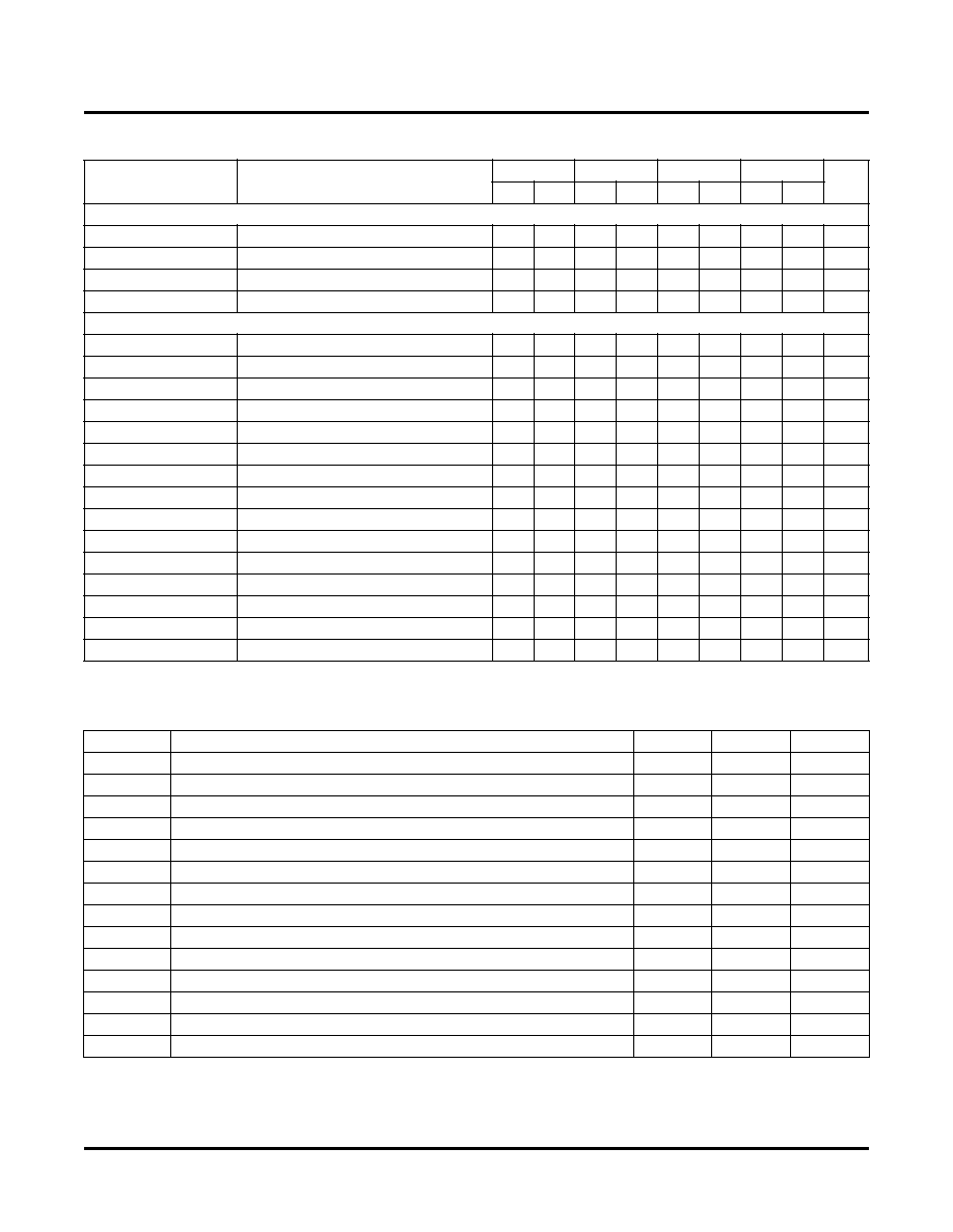
Lattice Semiconductor
ispMACH 5000B Family Data Sheet
34
ispMACH 5512B Timing Adders (Cont.)
Boundary Scan Timing Specifications
Adder
Type
-45
-75
-10
-12
Units
Base Parameter
Min. Max. Min. Max. Min. Max. Min. Max.
t
IOI
Input Adders
CLK0
t
GCLK_IN
-
0.00
-
0.00
-
0.00
-
0.00
ns
CLK1
t
GCLK_IN
-
0.20
-
0.20
-
0.20
-
0.20
ns
CLK2
t
GCLK_IN
-
0.20
-
0.20
-
0.20
-
0.20
ns
CLK3
t
GCLK_IN
-
0.20
-
0.20
-
0.20
-
0.20
ns
t
BLA
Additional Block Loading Adders
1
t
ROUTE
-
0.30
-
0.30
-
0.30
-
0.30
ns
2
t
ROUTE
-
0.70
-
0.70
-
0.70
-
0.70
ns
3
t
ROUTE
-
0.90
-
0.90
-
0.90
-
0.90
ns
4
t
ROUTE
-
1.10
-
1.10
-
1.10
-
1.10
ns
5
t
ROUTE
-
1.20
-
1.20
-
1.20
-
1.20
ns
6
t
ROUTE
-
1.30
-
1.30
-
1.30
-
1.30
ns
7
t
ROUTE
-
1.50
-
1.50
-
1.50
-
1.50
ns
8
t
ROUTE
-
1.60
-
1.60
-
1.60
-
1.60
ns
9
t
ROUTE
-
1.80
-
1.80
-
1.80
-
1.80
ns
10
t
ROUTE
-
1.90
-
1.90
-
1.90
-
1.90
ns
11
t
ROUTE
-
2.10
-
2.10
-
2.10
-
2.10
ns
12
t
ROUTE
-
2.40
-
2.40
-
2.40
-
2.40
ns
13
t
ROUTE
-
2.60
-
2.60
-
2.60
-
2.60
ns
14
t
ROUTE
-
2.90
-
2.90
-
2.90
-
2.90
ns
15
t
ROUTE
-
3.00
-
3.00
-
3.00
-
3.00
ns
Note: Open drain timing is the same as corresponding LVCMOS timing.
Timing v.1.1
Symbol
Parameter
Min.
Max.
Units
t
BTCP
TCK [BSCAN test] clock pulse width
125
--
ns
t
BTCH
TCK [BSCAN test] pulse width high
62.5
--
ns
t
BTCL
TCK [BSCAN test] pulse width low
62.5
--
ns
t
BTSU
TCK [BSCAN test] setup time
25
--
ns
t
BTH
TCK [BSCAN test] hold time
25
--
ns
t
BRF
TCK [BSCAN test] rise and fall time
50
--
mV/ns
t
BTCO
TAP controller falling edge of clock to valid output
--
25
ns
t
BTOZ
TAP controller falling edge of clock to data output disable
--
25
ns
t
BTVO
TAP controller falling edge of clock to data output enable
--
25
ns
t
BVTCPSU
BSCAN test Capture register setup time
25
--
ns
t
BTCPH
BSCAN test Capture register hold time
25
--
ns
t
BTUCO
BSCAN test Update reg, falling edge of clock to valid output
--
50
ns
t
BTUOZ
BSCAN test Update reg, falling edge of clock to output disable
--
50
ns
t
BTUOV
BSCAN test Update reg, falling edge of clock to output enable
--
50
ns

Lattice Semiconductor
ispMACH 5000B Family Data Sheet
35
Power Consumption
Power Estimation Coefficients
The device power, I
DEVICE,
is calculated from the following equation:
I
DEVICE
= I
DEVICE-AC
+ I
DEVICE-DC
Each term in I
DEVICE
is further defined as:
I
DEVICE-AC
= F
AVE
[(K0 * PT
HP
) + (K1 * PT
LP
) + K2 * GRP
LINES
)]
I
DEVICE-DC
= K3 * PT
HP
+ K4 * PT
LP
+ I
DC
+ I
DCO
where:
PT
HP
= Number of product terms in high power
PT
LP
= Number of product terms in low power
F
AVE
= Average output frequency of switching product terms in MHz
K0 = average current per product term in high power/MHz
K1 = average current per product term in low power/MHz
K2 = average current per GRP line/MHz
K3 = DC current per product term in high power
K4 = DC current per product term in low power
I
DC
= Static Device Current
I
DCO
= Static I/O Bank Current
I
CC
estimates are based on typical conditions (V
CC
= 2.5V, 25∞C). These values are for estimates only. Since the
value of I
CC
is sensitive to operating conditions and the program in the device, the actual I
CC
should be verified.
Device
K0
K1
K2
K3
K4
I
DC
(mA)
I
DCO
(mA)
ispMACH 5128B
0.0055
0.0055
0.005
0.273
0.091
10.6
1.2
ispMACH 5256B
0.0055
0.0055
0.005
0.2215
0.075
10.5
1.2
ispMACH 5384B
0.0055
0.0055
0.0065
0.2215
0.075
18.4
1.2
ispMACH 5512B
0.0055
0.0055
0.008
0.2215
0.075
22.9
1.2
Note: For further information about the use of these coefficients, refer to Lattice technical note number TN1023, Power Estimation in ispMACH
5000B Devices
.
ispMACH 5256B (High Power Mode)
ispMACH 5256B (Low Power Mode)
ispMACH 5000B Typical I
CC
vs. Frequency
ispMACH 5512B (High Power Mode)
ispMACH 5512B (Low Power Mode)
ispMACH 5384B (High Power Mode)
ispMACH 5384B (Low Power Mode)
0
100
200
300
400
500
600
0
50
100
150
200
250
300
f
MAX
(MHz)
I
CC
(mA)
Note: The devices are configured with maximum number of
16-bit counters, typical current at 2.5V, 25∞C.
ispMACH 5128B (High Power Mode)
ispMACH 5128B (Low Power Mode)

Lattice Semiconductor
ispMACH 5000B Family Data Sheet
36
Switching Test Conditions
Figure 9 shows the output test load that is used for AC testing. The specific values for resistance, capacitance, volt-
age, and other test conditions are shown in Table 3.
Figure 9. Output Test Load, LVTTL and LVCMOS Standards
Table 3. Test Fixture Required Components
Output test conditions for all other interfaces are determined by the respective standards.
Test Condition
R
1
R
2
C
L
Timing Ref.
V
CCO
Default LVCMOS 2.5 I/O (L -> H, H -> L)
188
188
35pF
V
CCO
/2
2.3V
Other LVCMOS Settings (L -> H, H -> L)
35pF
LVCMOS 3.3 = 1.5V
LVCMOS 3.3 = 3.0V
LVCMOS 2.5 = V
CCO
/2
LVCMOS 2.5 = 2.3V
LVCMOS 1.8 = V
CCO
/2
LVCMOS 1.8 = 1.65V
Default LVCMOS 2.5 I/O (Z -> H)
188
35pF
V
CCO
/2
2.3V
Default LVCMOS 2.5 I/O (Z -> L)
188
35pF
V
CCO
/2
2.3V
Default LVCMOS 2.5 I/O (H -> Z)
188
5pF
V
OH
- 0.15
2.3V
Default LVCMOS 2.5 I/O (L -> Z)
188
5pF
V
OL
+ 0.15
2.3V
V
CCO
R1
R2
CL
*
DUT
Test
Point
*
CL includes Test Fixture and Probe Capacitance.
0213A/ispm5kb
Lattice Semiconductor
ispMACH 5000B Family Data Sheet
37
Signal Descriptions
Signal Names
Description
TMS
Input - This pin is the Test Mode Select input, which is used to control the IEEE 1149.1 state machine.
TCK
Input - This pin is the Test Clock input pin, used to clock the IEEE 1149.1 state machine.
TDI
Input - This pin is the IEEE 1149.1 Test Data In pin, used to load data.
TDO
Output - This pin is the IEEE 1149.1 Test Data Out pin used to shift data out.
TOE
Input - Test Output Enable pin. TOE tristates all I/O pins when a logic low is driven.
GOE0, GOE1
Input - These two pins are the Global Output Enable input pins.
RESETB
Dedicated Reset Input - This pin resets all registers in the devices. The global polarity (active high or low
input) for this pin is selectable.
yzz
Input/Output ≠ These are the general purpose I/O used by the logic array. y is the GLB reference (alpha)
and z is the macrocell reference (numeric). z: 0-31
ispMACH 5128B
y: A-D, z: 0-31
ispMACH 5256B
y: A-H, z: 0-31
ispMACH 5384B
y: A-L, z: 0-31
ispMACH 5512B
y: A-P, z: 0-31
GND
Ground
NC
No connect
V
CC
Vcc - These are the power supply pins for the logic core.
GCLK0, GCLK1,
GCLK2, GCLK3
Inputs - These pins are dedicated CLK inputs.
V
REF0
, V
REF1
,
V
REF2
, V
REF3
Inputs - These are the reference supplies for the I/O banks.
V
CCO0
, V
CCO1
,
V
CCO2
, V
CCO3
V
CC
- These are the V
CC
supplies for each I/O bank.

Lattice Semiconductor
ispMACH 5000B Family Data Sheet
38
ispMACH 5000B Power Supply and NC Connections
Signal
128-Pin TQFP
1,2
208-Pin PQFP
1,2
256-Ball fpBGA
3
484-Ball fpBGA
3
VCC
13, 45, 77, 109
11, 48, 74, 115, 152,
178
F8, F9, H6, H11, J6, J11, L8,
L9
B2, B6, B17, B21, C9, C14, E5, E18,
F2, F21, J3, J20, P3, P20, U2, U21,
Y9, Y14, AA2, AA6, AA17, AA21
VCCO0
5, 120
5256B: 18, 189, 203
5384B/5512B: 7, 18,
189, 203
C3, C7, G3
B5, D7, E2, E6, E9, F5, G4, J5
VCCO1
28, 41
41, 56, 70
K3, P3, P7
P5, U5, V6, V9, Y3,
VCCO2
56, 69
5256B: 85, 99, 122
5384B/5512B: 85, 99,
109, 122
K14, P10, P14
P18, U18, V14, V17, Y20,
VCCO3
92, 105
145, 160, 174
C10, C14, G14
B18, D16, E14, E17, E21, F18, G19,
J18
VREF0
124
193
E7
A9
VREF1
37
66
M7
AA10
VREF2
61
90
R13
AA13
VREF3
100
169
A8
A15
GND
6, 20, 27, 40, 52,
57, 70, 84, 91,
104, 116, 121
5256B: 19, 20, 39, 40,
55, 69, 81, 86, 100,
123, 124, 143, 144,
159, 173, 185, 190,
204
5384B/5512B: 8, 19,
20, 39, 40, 55, 69, 81,
86, 100, 110, 123, 124,
143, 144, 159, 173,
185, 190, 204
A1, C5, C12, E3, E14, G7,
G8, G9, G10, H8, H9, H10,
J7, J8, J9, K7, K8, K9, K10,
M3, M14, P5, P12
A1, A22, C3, C20, D4, D19, E7, E16,
G5, G7, G8, G9, G10, G11, G12, G13,
G14, G15, G16, G18, H7, H8, H9, H10,
H11, H12, H13, H14, H15, H16, J7, J8,
J9, J10, J11, J12, J13, J14, J15, J16,
K7, K8, K9, K10, K11, K12, K13, K14,
K15, K16, L8, L9, L10, L11, L12, L13,
L14, L15, M7, M8, M9, M10, M11,
M12, M13, M14, M15, M16, N7, N8,
N9, N10, N11, N12, N13, N14, N15,
N16, P7, P8, P9, P10, P11, P12, P13,
P14, P15, P16, R7, R8, R9, R10, R11,
R12, R13, R14, R15, R16, T4, T7, T8,
T9, T10, T11, T12, T13, T14, T15, T16,
T19, W7, W16, AB1, AB22
NC
4
5128B: 45, 52,
109, 116
5256B: 1, 2, 7, 8, 101,
102, 103, 104, 105,
106, 109, 110, 205,
206, 207, 208
5256B: A11, A12, A13, A14,
B1, B2, B11, B12, B13, B16,
C1, C2, C13, C15, C16, D14,
D15, D16, E13, E15, F6, F7,
F10, F11, G6, G11, H1, H7,
H16, J1, J10, K6, K11, L5,
L6, L7, L10, L11, M4, N2,
N3, N4, N5, P1, P2, P4, P6,
P15, P16, R4, R5, R6, R15,
R16, T4, T5, T6
5384B: A11, A12, A13, B13,
C13, H1, H7, H16, J1, J10,
P6, R5, R6, T5, T6
5512B: H1, H7, H16, J1, J10
5512B: A6, A7, A8, A19, A20, A21, B7,
B8, B19, B20, B22, C7, C8, C10, C16,
C17, D9, D15, D18, E3, E10, F1, F3,
F4, F9, F10, F16, F17, F19, F20, G1,
G2, G3, G6, G17, G20, G21, G22, H1,
H2, H5, H6, H17, H18, H19, H20, H21,
H22, L6, L7, L16, N18, P4, AA1
1. All grounds must be electrically connected at the board level.
2. Not all grounds internally connected within the device. Pin orientation follows the conventional order from pin 1 marking of the top side view
and counter-clockwise.
3. Balls for ground (GND), VCC and VCCO signals are connected within the substrate. Pin orientation A1 starts from the upper left corner of
the top side view with alphabetical order ascending vertically and numerical order ascending horizontally.
4. No connects should not be connected to any active signals, VCC, VCCO, or GND.

Lattice Semiconductor
ispMACH 5000B Family Data Sheet
39
ispMACH 5128B, 5256B Logic Signal Connections: 128 TQFP
Pin Number
Bank
Number
ispMACH 5128B
ispMACH 5256B
GLB/MC/Pad
GLB/MC/Pad
1
0
D12
H16
2
0
D10
H14
3
0
D9
H12
4
0
D8
H10
5
0
VCCO (Bank 0)
VCCO (Bank 0)
6
0
GND (Bank 0)
GND (Bank 0)
7
0
D6
H8
8
0
D5
H6
9
0
D4
H5
10
0
D2
H4
11
0
D1
H2
12
0
D0
H0
13
-
VCC
VCC
14
0
GCLK0
GCLK0
15
1
GCLK1
GCLK1
16
-
TDI
TDI
17
-
TMS
TMS
18
-
TCK
TCK
19
-
TDO
TDO
20
-
GND
GND
21
1
A0
A0
22
1
A1
A2
23
1
A2
A4
24
1
A4
A5
25
1
A5
A6
26
1
A6
A8
27
1
GND (Bank 1)
GND (Bank 1)
28
1
VCCO (Bank 1)
VCCO (Bank 1)
29
1
A8
A10
30
1
A9
A12
31
1
A10
A14
32
1
A12
A16
33
1
A14
A20
34
1
A16
B10
35
1
A17
B12
36
1
A18
B14
37
1
A20/VREF1
B16/VREF1
38
1
A21
B18
39
1
A22
B20
40
1
GND (Bank 1)
GND (Bank 1)
41
1
VCCO (Bank 1)
VCCO (Bank 1)

Lattice Semiconductor
ispMACH 5000B Family Data Sheet
40
42
1
A24
B21
43
1
A25
B22
44
1
A26
B24
45
-
NC
VCC
46
1
A28
B26
47
1
A29
B28
48
1
A30
B30
49
2
B0
C0
50
2
B1
C2
51
2
B2
C4
52
-
NC
GND
53
2
B4
C5
54
2
B5
C6
55
2
B6
C8
56
2
VCCO (Bank 2)
VCCO (Bank 2)
57
2
GND (Bank 2)
GND (Bank 2)
58
2
B8
C10
59
2
B9
C12
60
2
B10
C14
61
2
B12/VREF2
C16/VREF2
62
2
B13
C18
63
2
B14
C20
64
2
B16
D10
65
2
B18
D14
66
2
B20
D16
67
2
B21
D18
68
2
B22
D20
69
2
VCCO (Bank 2)
VCCO (Bank 2)
70
2
GND (Bank 2)
GND (Bank 2)
71
2
B24
D21
72
2
B25
D22
73
2
B26
D24
74
2
B28
D26
75
2
B29
D28
76
2
B30
D30
77
-
VCC
VCC
78
-
TOE
TOE
79
2
RESETB
RESETB
80
2
GOE0
GOE0
81
2
GOE1
GOE1
82
2
GCLK2
GCLK2
83
3
GCLK3
GCLK3
84
-
GND
GND
ispMACH 5128B, 5256B Logic Signal Connections: 128 TQFP (Cont.)
Pin Number
Bank
Number
ispMACH 5128B
ispMACH 5256B
GLB/MC/Pad
GLB/MC/Pad

Lattice Semiconductor
ispMACH 5000B Family Data Sheet
41
85
3
C30
E30
86
3
C29
E28
87
3
C28
E26
88
3
C26
E24
89
3
C25
E22
90
3
C24
E21
91
3
GND (Bank 3)
GND (Bank 3)
92
3
VCCO (Bank 3)
VCCO (Bank 3)
93
3
C22
E20
94
3
C21
E18
95
3
C20
E16
96
3
C18
E14
97
3
C16
E10
98
3
C14
F20
99
3
C13
F18
100
3
C12/VREF3
F16/VREF3
101
3
C10
F14
102
3
C9
F12
103
3
C8
F10
104
3
GND (Bank 3)
GND (Bank 3)
105
3
VCCO (Bank 3)
VCCO (Bank 3)
106
3
C6
F8
107
3
C5
F6
108
3
C4
F5
109
-
NC
VCC
110
3
C2
F4
111
3
C1
F2
112
3
C0
F0
113
0
D30
G30
114
0
D29
G28
115
0
D28
G26
116
-
NC
GND
117
0
D26
G24
118
0
D25
G22
119
0
D24
G21
120
0
VCCO (Bank 0)
VCCO (Bank 0)
121
0
GND (Bank 0)
GND (Bank 0)
122
0
D22
G20
123
0
D21
G18
124
0
D20/VREF0
G16/VREF0
125
0
D18
G14
126
0
D17
G12
ispMACH 5128B, 5256B Logic Signal Connections: 128 TQFP (Cont.)
Pin Number
Bank
Number
ispMACH 5128B
ispMACH 5256B
GLB/MC/Pad
GLB/MC/Pad

Lattice Semiconductor
ispMACH 5000B Family Data Sheet
42
127
0
D16
G10
128
0
D14
H20
ispMACH 5256B, 5384B, 5512B Logic Signal Connections: 208 PQFP
Pin
Number
Bank
Number
ispMACH 5256B
ispMACH 5384B
ispMACH 5512B
GLB/MC/Pad
GLB/MC/Pad
GLB/MC/Pad
1
0
NC
K14
O30
2
0
NC
K12
O28
3
0
H30
K10
O26
4
0
H28
K8
O24
5
0
H26
K6
O22
6
0
H24
K4
O20
7
0
NC
VCCO
(Bank 0)
VCCO
(Bank 0)
8
0
NC
GND
(Bank 0)
GND
(Bank 0)
9
0
H22
K2
O18
10
0
H21
K0
O16
11
-
VCC
VCC
VCC
12
0
H20
L22
P22
13
0
H18
L20
P20
14
0
H16
L18
P18
15
0
H14
L16
P16
16
0
H12
L14
P14
17
0
H10
L12
P12
18
0
VCC
(Bank 0)
VCCO
(Bank 0)
VCCO
(Bank 0)
19
-
GND
GND
GND
20
0
GND
(Bank 0)
GND
(Bank 0)
GND
(Bank 0)
21
0
H8
L10
P10
22
0
H6
L8
P8
23
0
H5
L6
P6
24
0
H4
L4
P4
25
0
H2
L2
P2
26
0
H0
L0
P0
27
0
GCLK0
GCLK0
GCLK0
28
1
GCLK1
GCLK1
GCLK1
29
-
TDI
TDI
TDI
30
-
TMS
TMS
TMS
31
-
TCK
TCK
TCK
32
-
TDO
TDO
TDO
ispMACH 5128B, 5256B Logic Signal Connections: 128 TQFP (Cont.)
Pin Number
Bank
Number
ispMACH 5128B
ispMACH 5256B
GLB/MC/Pad
GLB/MC/Pad

Lattice Semiconductor
ispMACH 5000B Family Data Sheet
43
33
1
A0
A0
A0
34
1
A2
A2
A2
35
1
A4
A4
A4
36
1
A5
A6
A6
37
1
A6
A8
A8
38
1
A8
A10
A10
39
1
GND
(Bank 1)
GND
(Bank 1)
GND
(Bank 1)
40
-
GND
GND
GND
41
1
VCCO
(Bank 1)
VCCO
(Bank 1)
VCCO
(Bank 1)
42
1
A10
A12
A12
43
1
A12
A14
A14
44
1
A14
A16
A16
45
1
A16
A18
A18
46
1
A18
A20
A20
47
1
A20
A22
A22
48
-
VCC
VCC
VCC
49
1
A21
B12
B12
50
1
A22
B14
B14
51
1
A24
B16
B16
52
1
A26
B18
B18
53
1
A28
B20
B20
54
1
A30
B21
B21
55
1
GND
(Bank 1)
GND
(Bank 1)
GND
(Bank 1)
56
1
VCCO
(Bank 1)
VCCO
(Bank 1)
VCCO
(Bank 1)
57
1
B0
C0
C20
58
1
B2
C2
C24
59
1
B4
C4
C26
60
1
B5
C5
C28
61
1
B6
C6
D0
62
1
B8
C8
D2
63
1
B10
C10
D4
64
1
B12
C12
D6
65
1
B14
C14
D8
66
1
B16/VREF1
C16/VREF1
D10/VREF1
67
1
B18
C18
D12
68
1
B20
C20
D16
69
1
GND
(Bank 1)
GND
(Bank 1)
GND
(Bank 1)
70
1
VCCO
(Bank 1)
VCCO
(Bank 1)
VCCO
(Bank 1)
ispMACH 5256B, 5384B, 5512B Logic Signal Connections: 208 PQFP (Cont.)
Pin
Number
Bank
Number
ispMACH 5256B
ispMACH 5384B
ispMACH 5512B
GLB/MC/Pad
GLB/MC/Pad
GLB/MC/Pad

Lattice Semiconductor
ispMACH 5000B Family Data Sheet
44
71
1
B21
C21
D18
72
1
B22
C22
D20
73
1
B24
C24
D22
74
-
VCC
VCC
VCC
75
1
B26
C26
D24
76
1
B28
C28
D26
77
1
B30
C30
D28
78
2
C0
D0
E0
79
2
C2
D2
E2
80
2
C4
D4
E4
81
-
GND
GND
GND
82
2
C5
D5
E6
83
2
C6
D6
E8
84
2
C8
D8
E10
85
2
VCCO
(Bank 2)
VCCO
(Bank 2)
VCCO
(Bank 2)
86
2
GND
(Bank 2)
GND
(Bank 2)
GND
(Bank 2)
87
2
C10
D10
E12
88
2
C12
D12
E16
89
2
C14
D14
E18
90
2
C16/VREF2
D16/VREF2
E20/VREF2
91
2
C18
D18
E22
92
2
C20
D20
E24
93
2
C21
D21
E26
94
2
C22
D22
E28
95
2
C24
D24
F0
96
2
C26
D26
F2
97
2
C28
D28
F4
98
2
C30
D30
F6
99
2
VCCO
(Bank 2)
VCCO
(Bank 2)
VCCO
(Bank 2)
100
2
GND
(Bank 2)
GND
(Bank 2)
GND
(Bank 2)
101
2
NC
E4
G4
102
2
NC
E6
G6
103
2
NC
E8
G8
104
2
NC
E10
G10
105
2
NC
E20
G20
106
2
NC
E22
G22
107
2
D0
E24
G24
108
2
D2
E26
G26
109
2
NC
VCCO
(Bank 2)
VCCO
(Bank 2)
ispMACH 5256B, 5384B, 5512B Logic Signal Connections: 208 PQFP (Cont.)
Pin
Number
Bank
Number
ispMACH 5256B
ispMACH 5384B
ispMACH 5512B
GLB/MC/Pad
GLB/MC/Pad
GLB/MC/Pad
Lattice Semiconductor
ispMACH 5000B Family Data Sheet
45
110
2
NC
GND
(Bank 2)
GND
(Bank 2)
111
2
D4
E28
G28
112
2
D5
E30
G30
113
2
D6
F0
H0
114
2
D8
F2
H2
115
-
VCC
VCC
VCC
116
2
D10
F8
H8
117
2
D12
F10
H10
118
2
D14
F12
H12
119
2
D16
F14
H14
120
2
D18
F16
H16
121
2
D20
F18
H18
122
2
VCCO
(Bank 2)
VCCO
(Bank 2)
VCCO
(Bank 2)
123
-
GND
GND
GND
124
2
GND
(Bank 2)
GND
(Bank 2)
GND
(Bank 2)
125
2
D21
F20
H20
126
2
D22
F22
H22
127
2
D24
F24
H24
128
2
D26
F26
H26
129
2
D28
F28
H28
130
2
D30
F30
H30
131
-
TOE
TOE
TOE
132
2
RESETB
RESETB
RESETB
133
2
GOE0
GOE0
GOE0
134
2
GOE1
GOE1
GOE1
135
2
GCLK2
GCLK2
GCLK2
136
3
GCLK3
GCLK3
GCLK3
137
3
E30
G30
I30
138
3
E28
G28
I28
139
3
E26
G26
I26
140
3
E24
G24
I24
141
3
E22
G22
I22
142
3
E21
G20
I20
143
3
GND
(Bank 3)
GND
(Bank 3)
GND
(Bank 3)
144
-
GND
GND
GND
145
3
VCCO
(Bank 3)
VCCO
(Bank 3)
VCCO
(Bank 3)
146
3
E20
G18
I18
147
3
E18
G16
I16
148
3
E16
G14
I14
ispMACH 5256B, 5384B, 5512B Logic Signal Connections: 208 PQFP (Cont.)
Pin
Number
Bank
Number
ispMACH 5256B
ispMACH 5384B
ispMACH 5512B
GLB/MC/Pad
GLB/MC/Pad
GLB/MC/Pad
Lattice Semiconductor
ispMACH 5000B Family Data Sheet
46
149
3
E14
G12
I12
150
3
E12
G10
I10
151
3
E10
G8
I8
152
-
VCC
VCC
VCC
153
3
E8
H18
J0
154
3
E6
H16
K30
155
3
E5
H14
K28
156
3
E4
H12
K26
157
3
E2
H10
K24
158
3
E0
H8
K22
159
3
GND
(Bank 3)
GND
(Bank 3)
GND
(Bank 3)
160
3
VCCO
(Bank 3)
VCCO
(Bank 3)
VCCO
(Bank 3)
161
3
F30
I30
L30
162
3
F28
I28
L28
163
3
F26
I26
L26
164
3
F24
I24
L24
165
3
F22
I22
L22
166
3
F21
I21
L21
167
3
F20
I20
L20
168
3
F18
I18
L18
169
3
F16/VREF3
I16/VREF3
L16/VREF3
170
3
F14
I14
L14
171
3
F12
I12
L12
172
3
F10
I10
L10
173
3
GND
(Bank 3)
GND
(Bank 3)
GND
(Bank 3)
174
3
VCCO
(Bank 3)
VCCO
(Bank 3)
VCCO
(Bank 3)
175
3
F8
I8
L8
176
3
F6
I6
L6
177
3
F5
I5
L5
178
-
VCC
VCC
VCC
179
3
F4
I4
L4
180
3
F2
I2
L2
181
3
F0
I0
L0
182
0
G30
J30
M30
183
0
G28
J28
M28
184
0
G26
J26
M26
185
-
GND
GND
GND
186
0
G24
J24
M24
187
0
G22
J22
M22
188
0
G21
J21
M21
ispMACH 5256B, 5384B, 5512B Logic Signal Connections: 208 PQFP (Cont.)
Pin
Number
Bank
Number
ispMACH 5256B
ispMACH 5384B
ispMACH 5512B
GLB/MC/Pad
GLB/MC/Pad
GLB/MC/Pad
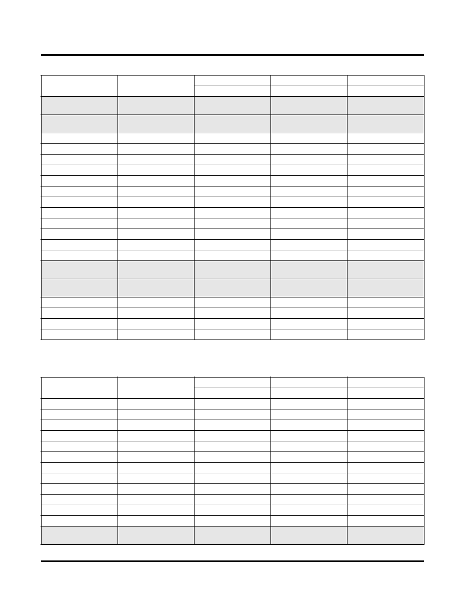
Lattice Semiconductor
ispMACH 5000B Family Data Sheet
47
189
0
VCCO
(Bank 0)
VCCO
(Bank 0)
VCCO
(Bank 0)
190
0
GND
(Bank 0)
GND
(Bank 0)
GND
(Bank 0)
191
0
G20
J20
M20
192
0
G18
J18
M18
193
0
G16/VREF0
J16/VREF0
M16/VREF0
194
0
G14
J14
M14
195
0
G12
J12
M12
196
0
G10
J10
M10
197
0
G8
J8
M8
198
0
G6
J6
M6
199
0
G5
J5
M5
200
0
G4
J4
M4
201
0
G2
J2
M2
202
0
G0
J0
M0
203
0
VCCO
(Bank 0)
VCCO
(Bank 0)
VCCO
(Bank 0)
204
0
GND
(Bank 0)
GND
(Bank 0)
GND
(Bank 0)
205
0
NC
K26
N8
206
0
NC
K24
N6
207
0
NC
K22
N5
208
0
NC
K20
N4
ispMACH 5256B, 5384B, 5512B Logic Signal Connections: 256 fpBGA
Ball
Number
Bank
Number
ispMACH 5256B
ispMACH 5384B
ispMACH 5512B
GLB/MC/Pad
GLB/MC/Pad
GLB/MC/Pad
A2
0
G5
J5
M5
A3
0
G10
J10
M10
A4
0
G20
J20
M20
A5
0
G26
J26
M26
B1
0
NC
K24
N6
B2
0
NC
K26
N8
B3
0
G4
J4
M4
B4
0
G12
J12
M12
B5
0
G21
J21
M21
B6
0
G28
J28
M28
C1
0
NC
K20
N4
C2
0
NC
K22
N5
C3
0
VCCO
(Bank 0)
VCCO
(Bank 0)
VCCO
(Bank 0)
ispMACH 5256B, 5384B, 5512B Logic Signal Connections: 208 PQFP (Cont.)
Pin
Number
Bank
Number
ispMACH 5256B
ispMACH 5384B
ispMACH 5512B
GLB/MC/Pad
GLB/MC/Pad
GLB/MC/Pad

Lattice Semiconductor
ispMACH 5000B Family Data Sheet
48
C4
0
G2
J2
M2
C6
0
G14
J14
M14
C7
0
VCCO
(Bank 0)
VCCO
(Bank 0)
VCCO
(Bank 0)
C8
0
G30
J30
M30
D1
0
H22
K2
O18
D2
0
H22
K4
O20
D3
0
H26
K6
O22
D4
0
H28
K8
O24
D5
0
H0
J0
M0
D6
0
H8
J8
M8
D7
0
H18
J18
M18
D8
0
H24
J24
M24
E1
0
H16
L18
P18
E2
0
H18
L20
P20
E4
0
H21
K0
O16
E5
0
H30
K10
O26
E6
0
G6
J6
M6
E7
0
G16/VREF0
J16/VREF0
M16/VREF0
E8
0
G22
J22
M22
F1
0
H5
L6
P6
F2
0
H10
L12
P12
F3
0
H12
L14
P14
F4
0
H14
L16
P16
F5
0
H20
L22
P22
F6
0
NC
K12
O28
F7
0
NC
K14
O30
G1
0
H2
L2
P2
G2
0
H4
L4
P4
G3
0
VCCO
(Bank 0)
VCCO
(Bank 0)
VCCO
(Bank 0)
G4
0
H6
L8
P8
G5
0
H8
L10
P10
G6
0
NC
L30
P30
H1
0
NC
NC
NC
H4
0
GCLK0
GCLK0
GCLK0
H5
0
H0
L0
P0
H7
0
NC
NC
NC
J1
1
NC
NC
NC
J4
1
GCLK1
GCLK1
GCLK1
J5
1
A5
A6
A6
K1
1
A0
A0
A0
K2
1
A2
A2
A2
ispMACH 5256B, 5384B, 5512B Logic Signal Connections: 256 fpBGA (Cont.)
Ball
Number
Bank
Number
ispMACH 5256B
ispMACH 5384B
ispMACH 5512B
GLB/MC/Pad
GLB/MC/Pad
GLB/MC/Pad

Lattice Semiconductor
ispMACH 5000B Family Data Sheet
49
K3
1
VCCO
(Bank 1)
VCCO
(Bank 1)
VCCO
(Bank 1)
K4
1
A8
A10
A10
K5
1
A16
A18
A18
K6
1
NC
A26
A26
L1
1
A4
A4
A4
L2
1
A6
A8
A8
L3
1
A12
A14
A14
L4
1
A14
A16
A16
L5
1
NC
A28
A28
L6
1
NC
B0
B0
L7
1
NC
B2
B2
M1
1
A10
A12
A12
M2
1
A18
A20
A20
M4
1
NC
B28
B28
M5
1
B0
C0
C20
M6
1
B6
C6
D0
M7
1
B16/VREF1
C16/VREF1
D10/VREF1
M8
1
B24
C24
D22
N1
1
A20
A22
A22
N2
1
NC
A30
A30
N3
1
NC
B6
B6
N4
1
NC
B26
B26
N5
1
NC
B30
B30
N6
1
B8
C8
D2
N7
1
B18
C18
D12
N8
1
B22
C22
D20
P1
1
NC
B4
B4
P2
1
NC
B5
B5
P3
1
VCCO
(Bank 1)
VCCO
(Bank 1)
VCCO
(Bank 1)
P4
1
NC
B22
B22
P6
1
NC
NC
C18
P7
1
VCC
(Bank 1)
VCCO
(Bank 1)
VCCO
(Bank 1)
P8
1
B20
C20
D16
R1
1
A21
B12
B12
R10
1
B30
C30
D28
R2
1
A26
B18
B18
R3
1
A30
B21
B21
R4
1
NC
B8
B8
R5
1
NC
NC
C0
R6
1
NC
NC
C16
ispMACH 5256B, 5384B, 5512B Logic Signal Connections: 256 fpBGA (Cont.)
Ball
Number
Bank
Number
ispMACH 5256B
ispMACH 5384B
ispMACH 5512B
GLB/MC/Pad
GLB/MC/Pad
GLB/MC/Pad

Lattice Semiconductor
ispMACH 5000B Family Data Sheet
50
R7
1
B10
C10
D4
R8
1
B5
C5
C28
R9
1
B21
C21
D18
T1
1
A22
B14
B14
T10
1
B14
C14
D8
T11
1
B26
C26
D24
T12
1
B28
C28
D26
T2
1
A24
B16
B16
T3
1
A28
B20
B20
T4
1
NC
B24
B24
T5
1
NC
NC
C2
T6
1
NC
NC
C12
T7
1
B2
C2
C24
T8
1
B4
C4
C26
T9
1
B12
C12
D6
H14
2
GCLK2
GCLK2
GCLK2
H15
2
GOE1
GOE1
GOE1
J10
2
NC
NC
NC
J14
2
RESETB
RESETB
RESETB
J15
2
GOE0
GOE0
GOE0
J16
2
D28
F28
H28
K11
2
NC
E8
G8
K12
2
D30
F30
H30
K13
2
D22
F22
H22
K14
2
VCCO
(Bank 2)
VCCO
(Bank 2)
VCCO
(Bank 2)
K15
2
D24
F24
H24
K16
2
D26
F26
H26
L10
2
NC
E4
G4
L11
2
NC
E6
G6
L12
2
D21
F20
H20
L13
2
D18
F16
H16
L14
2
D20
F18
H18
L15
2
D16
F14
H14
L16
2
D14
F12
H12
M10
2
C14
D14
E18
M11
2
C21
D21
E26
M12
2
D8
F2
H2
M13
2
D10
F8
H8
M15
2
D12
F10
H10
M16
2
D6
F0
H0
M9
2
C6
D6
E8
N10
2
C12
D12
E16
ispMACH 5256B, 5384B, 5512B Logic Signal Connections: 256 fpBGA (Cont.)
Ball
Number
Bank
Number
ispMACH 5256B
ispMACH 5384B
ispMACH 5512B
GLB/MC/Pad
GLB/MC/Pad
GLB/MC/Pad
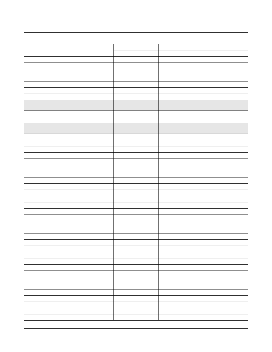
Lattice Semiconductor
ispMACH 5000B Family Data Sheet
51
N11
2
C22
D22
E28
N12
2
C30
D30
F6
N13
2
D2
E26
G26
N14
2
D0
E24
G24
N15
2
D4
E28
G28
N16
2
D5
E30
G30
N9
2
C5
D5
E6
P10
2
VCCO
(Bank 2)
VCCO
(Bank 2)
VCCO
(Bank 2)
P11
2
C10
D10
E12
P13
2
C24
D24
F0
P14
2
VCCO
(Bank 2)
VCCO
(Bank 2)
VCCO
(Bank 2)
P15
2
NC
E18
G18
P16
2
NC
E22
G22
P9
2
C0
D0
E0
R11
2
C2
D2
E2
R12
2
C8
D8
E10
R13
2
C16/VREF2
D16/VREF2
E20/VREF2
R14
2
C20
D20
E24
R15
2
NC
E10
G10
R16
2
NC
E20
G20
T13
2
B4
D4
E4
T14
2
B18
D18
E22
T15
2
B26
D26
F2
T16
2
B28
D28
F4
A10
3
F30
I30
L30
A14
3
NC
H0
K14
A15
3
E4
H12
K26
A16
3
E6
H16
K30
A6
3
F2
I2
L2
A7
3
F10
I10
L10
A8
3
F16/VREF3
I16/VREF3
L16/VREF3
A9
3
F26
I26
L26
B10
3
F21
I21
L21
B11
3
NC
G0
I0
B12
3
NC
H28
J12
B14
3
E0
H8
K22
B15
3
E5
H14
K28
B16
3
NC
H6
K21
B7
3
F0
I0
L0
B8
3
F4
I4
L4
B9
3
F20
I20
L20
ispMACH 5256B, 5384B, 5512B Logic Signal Connections: 256 fpBGA (Cont.)
Ball
Number
Bank
Number
ispMACH 5256B
ispMACH 5384B
ispMACH 5512B
GLB/MC/Pad
GLB/MC/Pad
GLB/MC/Pad
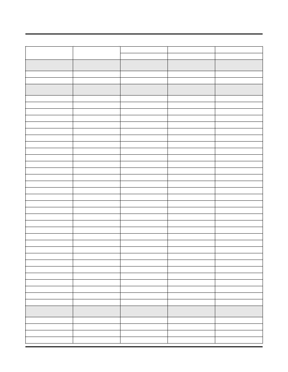
Lattice Semiconductor
ispMACH 5000B Family Data Sheet
52
C10
3
VCCO
(Bank 3)
VCCO
(Bank 3)
VCCO
(Bank 3)
C11
3
F28
I28
L28
C13
3
NC
NC
K12
C14
3
VCCO
(Bank 3)
VCCO
(Bank 3)
VCCO
(Bank 3)
C15
3
NC
H4
K18
C16
3
NC
H5
K20
C9
3
F8
I8
L8
D10
3
F14
I14
L14
D11
3
F22
I22
L22
D12
3
F24
I24
L24
D13
3
E2
H10
K24
D14
3
NC
H2
K16
A11
3
NC
NC
K0
A12
3
NC
NC
K2
A13
3
NC
NC
K4
B13
3
NC
NC
K10
D15
3
NC
H24
J8
D16
3
NC
H20
J2
D9
3
F5
I5
L5
E10
3
F12
I12
L12
E11
3
F18
I18
L18
E12
3
E8
H18
J0
E13
3
NC
H30
J14
E15
3
NC
H26
J10
E16
3
E10
G8
I8
E9
3
F6
I6
L6
F10
3
NC
G2
I2
F11
3
NC
G4
I4
F12
3
E12
G10
I10
F13
3
E16
G14
I14
F14
3
E14
G12
I12
F15
3
E18
G16
I16
F16
3
E20
G18
I18
G11
3
NC
G6
I6
G12
3
E22
G22
I22
G13
3
E21
G20
I20
G14
3
VCCO
(Bank 3)
VCCO
(Bank 3)
VCCO
(Bank 3)
G15
3
E26
G26
I26
G16
3
E28
G28
I28
H12
3
E24
G24
I24
H13
3
GCLK3
GCLK3
GCLK3
ispMACH 5256B, 5384B, 5512B Logic Signal Connections: 256 fpBGA (Cont.)
Ball
Number
Bank
Number
ispMACH 5256B
ispMACH 5384B
ispMACH 5512B
GLB/MC/Pad
GLB/MC/Pad
GLB/MC/Pad

Lattice Semiconductor
ispMACH 5000B Family Data Sheet
53
H16
3
NC
NC
NC
J12
3
E30
G30
I30
A1
-
GND
GND
GND
C12
-
GND
GND
GND
C5
-
GND
GND
GND
E14
-
GND
GND
GND
E3
-
GND
GND
GND
F8
-
VCC
VCC
VCC
F9
-
VCC
VCC
VCC
G10
-
GND
GND
GND
G7
-
GND
GND
GND
G8
-
GND
GND
GND
G9
-
GND
GND
GND
H10
-
GND
GND
GND
H11
-
VCC
VCC
VCC
H2
-
TMS
TMS
TMS
H3
-
TDI
TDI
TDI
H6
-
VCC
VCC
VCC
H8
-
GND
GND
GND
H9
-
GND
GND
GND
J11
-
VCC
VCC
VCC
J13
-
TOE
TOE
TOE
J2
-
TDO
TDO
TDO
J3
-
TCK
TCK
TCK
ispMACH 5512B Logic Signal Connections: 484 fpBGA
Ball
Number
Bank
Number
ispMACH 5512B
GLB/MC/Pad
J1
0
O30
K1
0
O28
H3
0
O26
J2
0
O24
H4
0
O22
K2
0
O20
B5
0
VCCO (Bank 0)
D19
0
GND
J6
0
O18
L1
0
O16
AA17
-
VCC
N2
0
P22
M3
0
P20
ispMACH 5256B, 5384B, 5512B Logic Signal Connections: 256 fpBGA (Cont.)
Ball
Number
Bank
Number
ispMACH 5256B
ispMACH 5384B
ispMACH 5512B
GLB/MC/Pad
GLB/MC/Pad
GLB/MC/Pad
Lattice Semiconductor
ispMACH 5000B Family Data Sheet
54
L5
0
P18
R1
0
P16
P2
0
P14
N3
0
P12
D7
0
VCCO (Bank 0)
A1
-
GND
D4
-
GND
M6
0
P10
M5
0
P8
M4
0
P6
N4
0
P4
N6
0
P2
N5
0
P0
P6
0
GCLK0
R6
1
GCLK1
R2
-
TDI
T1
-
TMS
R3
-
TCK
R4
-
TDO
R5
1
A0
T2
1
A2
T5
1
A4
T3
1
A6
U1
1
A8
U4
1
A10
G10
-
GND
A22
-
GND
P5
1
VCCO (Bank 1)
V1
1
A12
U3
1
A14
V5
1
A16
V2
1
A18
W1
1
A20
V3
1
A22
AA2
-
VCC
AA4
1
B12
W6
1
B14
V4
1
B16
U7
1
B18
AB2
1
B20
V7
1
B21
G11
-
GND
U5
1
VCCO (Bank 1)
ispMACH 5512B Logic Signal Connections: 484 fpBGA (Cont.)
Ball
Number
Bank
Number
ispMACH 5512B
GLB/MC/Pad

Lattice Semiconductor
ispMACH 5000B Family Data Sheet
55
U8
1
C20
AB7
1
C24
U9
1
C26
AA9
1
C28
W9
1
D0
AB8
1
D2
U10
1
D4
AB9
1
D6
V11
1
D8
AA10
1
D10/VREF1
V10
1
D12
AB10
1
D16
G12
1
GND
V6
1
VCCO (Bank 1)
W10
1
D18
W11
1
D20
U11
1
D22
AA21
-
VCC
AA11
1
D24
V12
1
D26
AB11
1
D28
W12
2
E0
Y11
2
E2
Y12
2
E4
AB1
-
GND
AB12
2
E6
U12
2
E8
AA12
2
E10
P18
2
VCCO (Bank 2)
G13
-
GND
Y13
2
E12
AB13
2
E16
W13
2
E18
AA13
2
E20/VREF2
U13
2
E22
AB14
2
E24
V13
2
E26
AA14
2
E28
U14
2
F0
AB15
2
F2
Y15
2
F4
AB16
2
F6
U18
2
VCCO (Bank 2)
ispMACH 5512B Logic Signal Connections: 484 fpBGA (Cont.)
Ball
Number
Bank
Number
ispMACH 5512B
GLB/MC/Pad
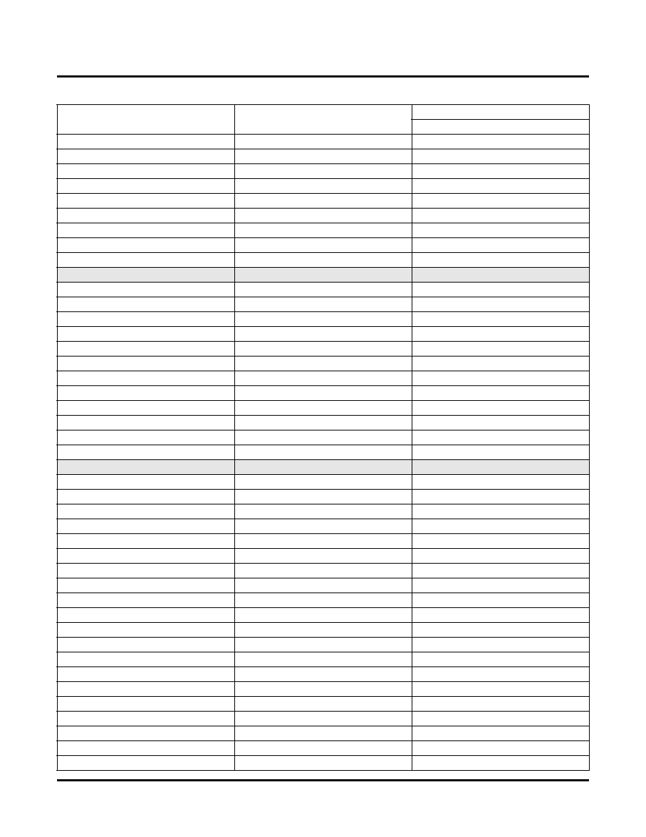
Lattice Semiconductor
ispMACH 5000B Family Data Sheet
56
G14
-
GND
U15
2
G4
W17
2
G6
U16
2
G8
AA19
2
G10
AA20
2
G20
W19
2
G22
Y19
2
G24
V19
2
G26
V14
2
VCCO (Bank 2)
G15
-
GND
Y21
2
G28
W20
2
G30
AA22
2
H0
W21
2
H2
AA6
-
VCC
V21
2
H8
W22
2
H10
V18
2
H12
U20
2
H14
V22
2
H16
U19
2
H18
V17
2
VCCO (Bank 2)
AB22
-
GND
G16
-
GND
U17
2
H20
U22
2
H22
T20
2
H24
T21
2
H26
T17
2
H28
R20
2
H30
T18
-
TOE
R19
2
RESETB
R18
2
GOE0
R17
2
GOE1
P17
2
GCLK2
P19
3
GCLK3
R21
3
I30
T22
3
I28
P21
3
I26
N20
3
I24
R22
3
I22
N21
3
I20
ispMACH 5512B Logic Signal Connections: 484 fpBGA (Cont.)
Ball
Number
Bank
Number
ispMACH 5512B
GLB/MC/Pad

Lattice Semiconductor
ispMACH 5000B Family Data Sheet
57
G18
-
GND
C20
-
GND
B18
3
VCCO (Bank 3)
M18
3
I18
N19
3
I16
P22
3
I14
M20
3
I12
N22
3
I10
N17
3
I8
B17
-
VCC
J21
3
J0
F22
3
K30
E22
3
K28
E19
3
K26
E20
3
K24
D22
3
K22
G5
-
GND
D16
3
VCCO (Bank 3)
A16
3
L30
F14
3
L28
C15
3
L26
D13
3
L24
E15
3
L22
F13
3
L21
B14
3
L20
E13
3
L18
A15
3
L16/VREF3
D12
3
L14
A14
3
L12
B13
3
L10
G7
-
GND
E14
3
VCCO (Bank 3)
A13
3
L8
B12
3
L6
C13
3
L5
B2
-
VCC
A12
3
L4
C12
3
L2
A11
3
L0
D11
0
M30
B11
0
M28
E12
0
M26
C3
-
GND
ispMACH 5512B Logic Signal Connections: 484 fpBGA (Cont.)
Ball
Number
Bank
Number
ispMACH 5512B
GLB/MC/Pad

Lattice Semiconductor
ispMACH 5000B Family Data Sheet
58
C11
0
M24
F12
0
M22
B10
0
M21
E2
0
VCCO (Bank 0)
E16
-
GND
A10
0
M20
D10
0
M18
A9
0
M16/VREF0
E11
0
M14
B9
0
M12
F11
0
M10
E8
0
M8
A5
0
M6
F8
0
M5
C6
0
M4
D8
0
M2
A3
0
M0
E6
0
VCCO (Bank 0)
E7
-
GND
C2
0
N8
C1
0
N6
D1
0
N5
D2
0
N4
W2
0
A24
Y1
0
A26
Y2
0
A28
W3
0
A30
B15
3
K0
C21
3
K10
D17
3
K12
C19
3
K14
C18
3
K16
C22
3
K18
A17
3
K2
D20
3
K20
D21
3
K21
F15
3
K4
A18
3
K5
D14
3
K6
B16
3
K8
E1
0
N0
E4
0
N10
C4
0
N12
ispMACH 5512B Logic Signal Connections: 484 fpBGA (Cont.)
Ball
Number
Bank
Number
ispMACH 5512B
GLB/MC/Pad
Lattice Semiconductor
ispMACH 5000B Family Data Sheet
59
D6
0
N14
B1
0
N16
D5
0
N18
D3
0
N2
B4
0
N20
B3
0
N21
F6
0
N22
C5
0
N24
F7
0
N26
A4
0
N28
A2
0
N30
K5
0
O0
L2
0
O10
J4
0
O12
K3
0
O14
L3
0
O2
K4
0
O4
K6
0
O6
M1
0
O8
L4
0
P24
P1
0
P26
M2
0
P28
N1
0
P30
AA3
1
B0
U6
1
B10
W4
1
B2
AA5
1
B22
AB3
1
B24
Y6
1
B26
AB4
1
B28
Y7
1
B30
W5
1
B4
Y4
1
B5
T6
1
B6
Y5
1
B8
AB5
1
C0
AB6
1
C10
W8
1
C12
AA8
1
C16
Y10
1
C18
V8
1
C2
AA7
1
C4
Y8
1
C8
ispMACH 5512B Logic Signal Connections: 484 fpBGA (Cont.)
Ball
Number
Bank
Number
ispMACH 5512B
GLB/MC/Pad

Lattice Semiconductor
ispMACH 5000B Family Data Sheet
60
W14
2
F10
AB17
2
F12
Y16
2
F16
AA16
2
F18
Y17
2
F20
AB18
2
F22
V15
2
F24
AB19
2
F26
W15
2
F28
AA15
2
F8
AB20
2
G0
V16
2
G12
AB21
2
G14
Y18
2
G16
W18
2
G18
AA18
2
G2
Y22
2
H4
V20
2
H6
L20
3
I0
L19
3
I2
M21
3
I4
M19
3
I6
K21
3
J10
L17
3
J12
K22
3
J14
K17
3
J16
L22
3
J18
J22
3
J2
K19
3
J20
L21
3
J22
L18
3
J24
K20
3
J26
M22
3
J28
M17
3
J30
J19
3
J4
J17
3
J6
K18
3
J8
B21
-
VCC
B6
-
VCC
C14
-
VCC
C9
-
VCC
E18
-
VCC
E5
-
VCC
ispMACH 5512B Logic Signal Connections: 484 fpBGA (Cont.)
Ball
Number
Bank
Number
ispMACH 5512B
GLB/MC/Pad
Lattice Semiconductor
ispMACH 5000B Family Data Sheet
61
F2
-
VCC
F21
-
VCC
J20
-
VCC
J3
-
VCC
P20
-
VCC
P3
-
VCC
U2
-
VCC
U21
-
VCC
Y14
-
VCC
Y9
-
VCC
E9
0
VCCO (Bank 0)
F5
0
VCCO (Bank 0)
G4
0
VCCO (Bank 0)
J5
0
VCCO (Bank 0)
V9
1
VCCO (Bank 1)
Y3
1
VCCO (Bank 1)
Y20
2
VCCO (Bank 2)
E17
3
VCCO (Bank 3)
E21
3
VCCO (Bank 3)
F18
3
VCCO (Bank 3)
G19
3
VCCO (Bank 3)
J18
3
VCCO (Bank 3)
ispMACH 5512B Logic Signal Connections: 484 fpBGA (Cont.)
Ball
Number
Bank
Number
ispMACH 5512B
GLB/MC/Pad

Lattice Semiconductor
ispMACH 5000B Family Data Sheet
62
Part Number Description
Ordering Information
Commercial
Device
Part Number
Macrocells
Voltage
t
PD
Package
Pin/Ball Count
I/O
Grade
LC5128B
LC5128B-3T128C
128
2.5
3.0
TQFP
128
92
C
LC5128B-5T128C
128
2.5
5.0
TQFP
128
92
C
LC5128B-75T128C
128
2.5
7.5
TQFP
128
92
C
LC5256B
LC5256B-4T128C
256
2.5
4.0
TQFP
128
92
C
LC5256B-4Q208C
256
2.5
4.0
PQFP
208
144
C
LC5256B-4F256C
256
2.5
4.0
fpBGA
256
144
C
LC5256B-5T128C
256
2.5
5.0
TQFP
128
92
C
LC5256B-5Q208C
256
2.5
5.0
PQFP
208
144
C
LC5256B-5F256C
256
2.5
5.0
fpBGA
256
144
C
LC5256B-75T128C
256
2.5
7.5
TQFP
128
92
C
LC5256B-75Q208C
256
2.5
7.5
PQFP
208
144
C
LC5256B-75F256C
256
2.5
7.5
fpBGA
256
144
C
LC5384B
LC5384B-4Q208C
384
2.5
4.0
PQFP
208
156
C
LC5384B-4F256C
384
2.5
4.0
fpBGA
256
186
C
LC5384B-5Q208C
384
2.5
5.0
PQFP
208
156
C
LC5384B-5F256C
384
2.5
5.0
fpBGA
256
186
C
LC5384B-75Q208C
384
2.5
7.5
PQFP
208
156
C
LC5384B-75F256C
384
2.5
7.5
fpBGA
256
186
C
Device Number
5128 = 128 Macrocells
5256 = 256 Macrocells
5384 = 384 Macrocells
5512 = 512 Macrocells
Supply Voltage
B = 2.5V
LC XXXXB ≠ XX X XXX X
Speed
3 = 3.0ns
4 = 4.0ns
45 = 4.5ns
5 = 5.0ns
75 = 7.5ns
10 = 10ns
12 = 12ns
Pin/Ball Count
128
208
256
484
Package
T = TQFP
Q = PQFP
F = fpBGA
Grade
C = Commercial
I = Industrial
Device Family
0212/ispm5b

Lattice Semiconductor
ispMACH 5000B Family Data Sheet
63
Industrial
LC5512B
LC5512B-45Q208C
512
2.5
4.5
PQFP
208
156
C
LC5512B-45F256C
512
2.5
4.5
fpBGA
256
196
C
LC5512B-45F484C
512
2.5
4.5
fpBGA
484
256
C
LC5512B-75Q208C
512
2.5
7.5
PQFP
208
156
C
LC5512B-75F256C
512
2.5
7.5
fpBGA
256
196
C
LC5512B-75F484C
512
2.5
7.5
fpBGA
484
256
C
LC5512B-10Q208C
512
2.5
10
PQFP
208
156
C
LC5512B-10F256C
512
2.5
10
fpBGA
256
196
C
LC5512B-10F484C
512
2.5
10
fpBGA
484
256
C
Note: The speed grade for these devices are dual marked. For example, the commercial grade -4xxxxC is also marked with the industrial
grade -5xxxxI. The commercial grade is always one speed grade faster than the associated dual mark industrial grade.
Device
Part Number
Macrocells
Voltage
t
PD
Package
Pin/Ball Count
I/O
Grade
LC5128B
LC5128B-5T128I
128
2.5
5.0
TQFP
128
92
I
LC5128B-75T128I
128
2.5
7.5
TQFP
128
92
I
LC5128B-10T128I
128
2.5
10
TQFP
128
92
I
LC5256B
LC5256B-5T128I
256
2.5
5.0
TQFP
128
92
I
LC5256B-5Q208I
256
2.5
5.0
PQFP
208
144
I
LC5256B-5F256I
256
2.5
5.0
fpBGA
256
144
I
LC5256B-75T128I
256
2.5
7.5
TQFP
128
92
I
LC5256B-75Q208I
256
2.5
7.5
PQFP
208
144
I
LC5256B-75F256I
256
2.5
7.5
fpBGA
256
144
I
LC5256B-10T128I
256
2.5
10
TQFP
128
92
I
LC5256B-10Q208I
256
2.5
10
PQFP
208
144
I
LC5256B-10F256I
256
2.5
10
fpBGA
256
144
I
LC5384B
LC5384B-5Q208I
384
2.5
5.0
PQFP
208
156
I
LC5384B-5F256I
384
2.5
5.0
fpBGA
256
186
I
LC5384B-75Q208I
384
2.5
7.5
PQFP
208
156
I
LC5384B-75F256I
384
2.5
7.5
fpBGA
256
186
I
LC5384B-10Q208I
384
2.5
10
PQFP
208
156
I
LC5384B-10F256I
384
2.5
10
fpBGA
256
186
I
LC5512B
LC5512B-75Q208I
512
2.5
7.5
PQFP
208
156
I
LC5512B-75F256I
512
2.5
7.5
fpBGA
256
196
I
LC5512B-75F484I
512
2.5
7.5
fpBGA
484
256
I
LC5512B-10Q208I
512
2.5
10
PQFP
208
156
I
LC5512B-10F256I
512
2.5
10
fpBGA
256
196
I
LC5512B-10F484I
512
2.5
10
fpBGA
484
256
I
LC5512B-12Q208I
512
2.5
12
PQFP
208
156
I
LC5512B-12F256I
512
2.5
12
fpBGA
256
196
I
LC5512B-12F484I
512
2.5
12
fpBGA
484
256
I
Note: The speed grade for these devices are dual marked. For example, the commercial grade -4xxxxC is also marked with the industrial
grade -5xxxxI. The commercial grade is always one speed grade faster than the associated dual mark industrial grade.
Commercial (Cont.)
Device
Part Number
Macrocells
Voltage
t
PD
Package
Pin/Ball Count
I/O
Grade

Lattice Semiconductor
ispMACH 5000B Family Data Sheet
64
For Further Information
In addition to this data sheet, the following technical notes may be helpful when designing with the ispMACH 5000B family:
∑ sysIO Design and Usage Guidelines (TN1000)
∑ Power Estimation in ispMACH 5000B Devices (TN1023)