
www.latticesemi.com
1
5kvg_09
ispMACH
5000VG Family
3.3V In-System Programmable
SuperBIG,
SuperWIDE
High Density PLDs
December 2001
Data Sheet
TM
TM
TM
Features
High Density
� 768 to 1,024 macrocells
� 196 to 384 I/Os
sysCLOCKTM PLL � Timing Control
� Multiply and divide factors between 1 and 32
� Clock shifting capability � 3.5ns in 500ps steps
� Multiple output frequencies
� External feedback capability for board-level
clock deskew
� LVDS/LVPECL clock input capability
High Speed Logic Implementation
� SuperWIDE 68-input logic block
� Up to 160 product terms per output
� Hierarchical routing structure provides fast inter-
connect
sysIOTM Capability
� LVCMOS 1.8, 2.5 and 3.3
� LVTTL
� SSTL 2 (I & II)
� SSTL 3 (I & II)
� CTT 3.3, CTT 2.5
� HSTL (I & III)
� PCI-X, PCI 3.3
� GTL+
� AGP-1X
� 5V tolerance
� Programmable drive strength
Ease of Design
� Product term sharing
� Extensive clocking and OE capability
Easy System Integration
� 3.3V power supply
� Hot socketing
� Input pull-up, pull-down or bus-keeper
� Open drain capability
� Slew rate control
� Macrocell-based power management
� IEEE 1149.1 boundary scan testable
� In-system programmable via IEEE 1532 ISC
compliant interface
ispMACH 5000VG Introduction
The ispMACH 5000VG represents the third generation
of Lattice's SuperWIDE CPLD architecture. Through
their wide 68-input blocks, these devices give signifi-
cantly improved speed performance for typical designs
over architectures with fewer inputs.
The ispMACH 5000VG takes the unique benefits of the
SuperWIDE architecture and extends it to higher densi-
ties referred to as SuperBIG, by using the combination
of an innovative product term architecture and a two-
tiered hierarchical routing architecture. Additionally,
sysCLOCK and sysIO capabilities have been added to
maximize system-level performance and integration.
Table 1. ispMACH 5000VG Family Selection Guide
ispMACH
5768VG
ispMACH
51024VG
Macrocells
768
1,024
User I/O Options
196/304
304/384
t
PD
(ns)
5.0
5.0
t
S
� Set-up with 0 Hold (ns)
3.0
3.0
t
CO
(ns)
4.4
4.4
f
MAX
(MHz)
178
178
Supply Voltage (V)
3.3V
3.3V
Package
256-ball fpBGA
484-ball fpBGA
484-ball fpBGA
676-ball fpBGA
Lattice Semiconductor
ispMACH 5000VG Family Data Sheet
2
Overview
The ispMACH 5000VG devices consist of multiple SuperWIDE 68-input, 32-macrocell Generic Logic Blocks
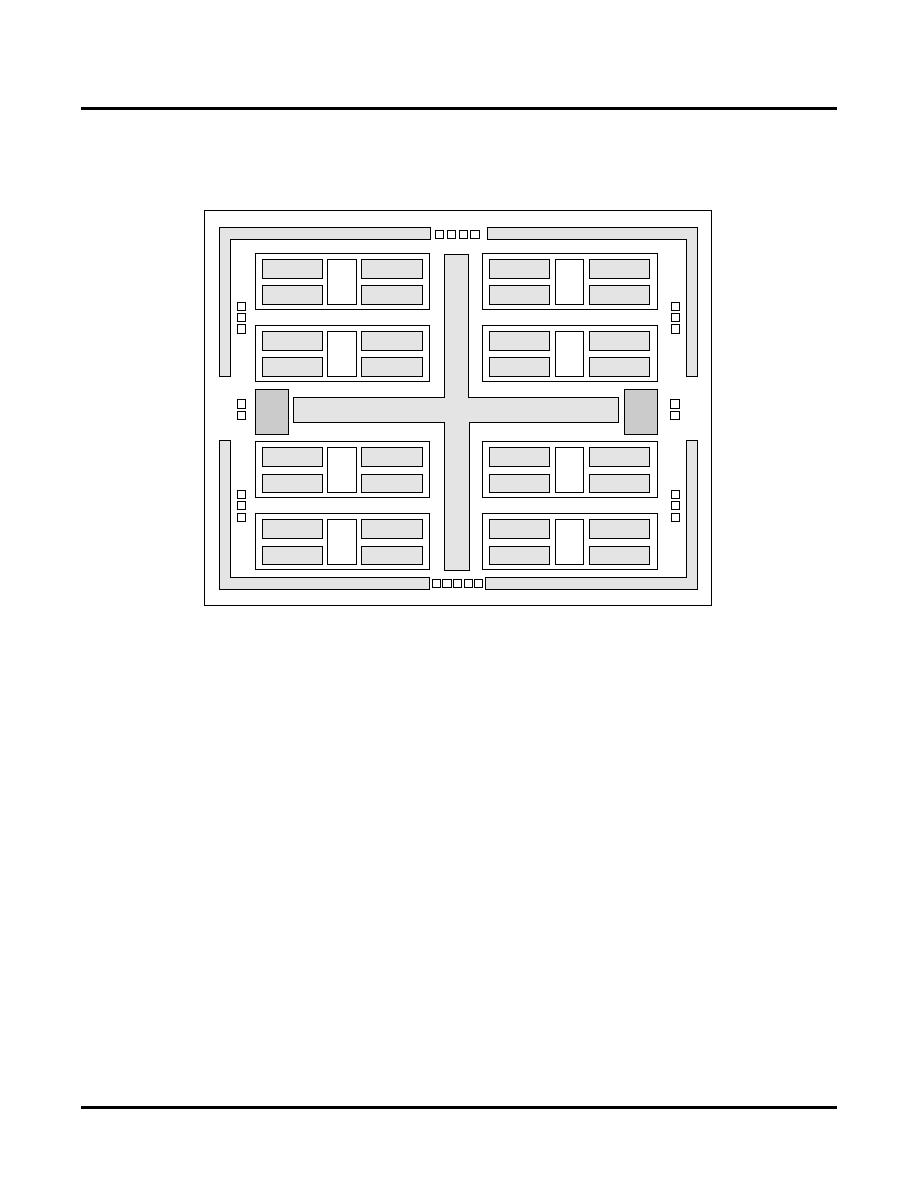
(GLBs) interconnected by a tiered routing system. Figure 1 shows the functional block diagram of the ispMACH
5000VG. Groups of four GLBs, referred to as segments, are interconnected via a Segment Routing Pool (SRP).
Segments are interconnected via the Global Routing Pool (GRP.) Together the GLBs and the routing pools allow
designers to create large designs in a single device without compromising performance.
Each GLB has 68 inputs coming from the SRP and contains 163 product terms. These product terms form groups
of five product term clusters, which feed the PT sharing array or the macrocell directly. The ispMACH 5000VG
allows up to 160 product terms to be connected to a single macrocell via the product term expanders and PT Shar-
ing Array.
The macrocell is designed to provide flexible clocking and control functionality with the capability to select between
global, product term and block-level resources. The outputs of the macrocells are fed back into the switch matrices
and, if required, the sysIO cell.
All I/Os in the ispMACH 5000VG family are sysIOs, which are split into four banks. Each bank has a separate I/O
power supply and reference voltage. The sysIO cells allow operation with a wide range of today's emerging inter-
face standards. Within a bank, inputs can be set to a variety of standards, providing the reference voltage require-
ments of the chosen standards are compatible. Within a bank, the outputs can be set to differing standards,
providing the I/O power supply voltage and the reference voltage requirements of the chosen standard are compat-
ible. Support for this wide range of standards allows designers to achieve significantly higher board-level perfor-
mance compared to the more traditional LVCMOS standards.
Figure 1. Functional Block Diagram
PLL0
PLL1
GLB
V
CCP0
V
CCO0
GCLK0
V
REF0
RESETB
GOE1
GOE2
TO
E
TDI
TDO
TMS
TCK
V
CCJ
I/O Bank 0
I/O Bank 3
I/O Bank 1
I/O Bank 2
GNDP0
V
CCP1
GNDP1
GLB
GLB
GLB
Global Routing Pool
SRP
SRP
SRP
SRP
SRP
SRP
SRP
SRP
V
CCO1
GCLK1
V
REF1
V
CCO3
GCLK3
V
REF3
V
CCO2
GCLK2
V
REF2
GLB
GLB
GLB
GLB
GLB
GLB
GLB
GLB
GLB
GLB
GLB
GLB
GLB
GLB
GLB
GLB
GLB
GLB
GLB
GLB
GLB
GLB
GLB
GLB
GLB
GLB
GLB
GLB

Lattice Semiconductor
ispMACH 5000VG Family Data Sheet
3
The ispMACH5000VG devices also contain sysCLOCK Phase Locked Loops (PLLs) that provide designers with
increased clocking flexibility. The PLLs can be used to synthesize new clocks for use on-chip or elsewhere within
the system. They can also be used to deskew clocks, again both at the chip and system levels. A variable delay line
capability further improves this and allows designers to retard or advance the clock in order to tune set-up and
clock-to-out times for optimal results. The ispMACH 5000VG Family Selection Guide (Table 1) details the key
attributes and packages for the ispMACH 5000VG devices.
ispMACH 5000VG Architecture
The ispMACH 5000VG Family of In-System Programmable High Density Logic Devices is based on segments con-
taining four Generic Logic Blocks (GLBs) and a hierarchical routing pool (GRP) structure interconnecting the seg-
ments. A segment routing pool (SRP) connects each GLB in a segment allowing the maximum flexibility and
speed.
Outputs from the GLBs drive the Segment Routing Pool (SRP) and the Global Routing Pool (GRP). Enhanced
switching resources are provided to allow signals in the Segment Routing Pool to drive any or all the GLBs in the
segment. Optimal switching is provided to allow all signals in the Global Routing Pool to be routed to any or all
SRPs. This mechanism allows fast, efficient connections across the entire device.
Segment
Each segment contains four GLBs and a segment routing pool (SRP). Each GLB has 32 internal feedback outputs
and 16 external feedback outputs, for a total of 48 outputs from each GLB feeding the SRP. The SRP contains up to
384 signals, 48 from each GLB and 192 from the GRP, with full routing capability. This routing scheme maximizes
the flexibility and speed of the device without sacrificing the routing.
Generic Logic Block
Each GLB contains 32 macrocells and a fully populated, programmable AND-array with 160 logic product terms
and three control product terms. The GLB has 68 inputs from the Segment Routing Pool, which are available in
both true and complement form for every product term. The three control product terms are used for shared reset,
clock and output enable functions. Figure 3 shows the structure of the GLB from the macrocell perspective. This is
referred to as a macrocell slice. There are 32 macrocell slices per GLB.
AND-Array
The programmable AND-Array consists of 68 inputs and 163 output product terms. The 68 inputs from the SRP are
used to form 136 lines in the AND-Array (true and complement of the inputs). Each line in the array can be con-
nected to any of the 163 output product terms via a wired AND. Each of the 160 logic product terms feed the Dual-
OR Array with the remaining three control product terms feeding the Shared PT Clock, Shared PT Reset and
Shared PT OE. Every set of five product terms from the 160 logic product terms forms a product term cluster start-
Figure 2. Segment
Clocks
4
GLB
Segment
Routing
Pool
(SRP)
48
68
48
48
68
48
68
68
48
48
192
From
GRP
To
GRP
To
GRP
To
GRP
Clocks
4
To
GRP
48
48
Clocks
4
Clocks
4
GLB
GLB
GLB

Lattice Semiconductor
ispMACH 5000VG Family Data Sheet
4
ing with PT0. There is one product term cluster for every macrocell in the GLB. In addition to the three control prod-
uct terms, the first, third, fourth and fifth product terms of each cluster can be used as a PTOE (output macrocells
only), PT Clock, PT Preset and PT Reset, respectively. Figure 4 is a graphical representation of the AND-Array.
Figure 3. Macrocell Slice
Figure 4. AND-Array
From
SRP
68
Speed/
Power
PTSA
From
n-7
To
n+7
PTSA Bypass
PT OE to
I/O Block
From
I/O Cell
PT Clock
PT Preset
PT Reset
Shared PT Reset
Shared PT Clock
BCLK0
BCLK1
BCLK2
BCLK3
Global Reset
Clk En
Clk
R/L
D
P
R
Q
AND Array
Dual-OR Array
Macrocell
Output
to I/O Block
GRP and SRP
PT0
PT1
Cluster 0
PT2
PT3
PT4
In[0]
In[66]
In[67]
Note:
Indicates programmable fuse.
PT160
PT161
PT162
Shared clock
Shared reset
Shared OE
PT156
PT157
PT158
PT159
PT155
Cluster 31

Lattice Semiconductor
ispMACH 5000VG Family Data Sheet
5
Enhanced Dual-OR Array
To facilitate logic functions requiring a very large number of product terms, the ispMACH 5000VG architecture has
been enhanced with an innovative product term expander capability. This capability is embedded in the Dual-OR
Array. The Dual-OR Array consists of 64 OR gates. There are two OR gates per macrocell in the GLB. These OR
gates are referred to as the Expandable PTSA OR gate and the PTSA-Bypass OR gate.
The PTSA-Bypass OR gate receives its five inputs from the combination of product terms associated with the prod-
uct term cluster. The PTSA-Bypass OR gate feeds the macrocell directly for fast narrow logic. The Expandable
PTSA OR gate receives five inputs from the combination of product terms associated with the product term cluster.
It also receives an additional input from the Expanded PTSA OR gate of the N-7 macrocell, where N is the number
of the macrocell associated with the current OR gate. The Expandable PTSA OR gate feeds the PTSA for sharing
with other product terms and the N+7 Expandable PTSA OR gate. This allows cascading of multiple OR gates for
wide functions. There is a small timing adder for each level of expansion. Figure 5 is a graphical representation of
the Enhanced Dual-OR Array.
Figure 5. Enhanced Dual-OR Array
From
n-7
To
n+7
From PT0
From PT1
From PT2
From PT3
From PT4
PTSA Bypass
To Macrocell
To I/O Block
To Macrocell
To Macrocell
To Macrocell
To PTSA
PT OE
PT Clock
PT Preset
PT Reset
n