www.latticesemi.com
1-1
Introduction_01.2
November 2004
Preliminary Data Sheet
� 2004 Lattice Semiconductor Corp. All Lattice trademarks, registered trademarks, patents, and disclaimers are as listed at www.latticesemi.com/legal. All other brand
or product names are trademarks or registered trademarks of their respective holders. The specifications and information herein are subject to change without notice.
Features
Extensive Density and Package Options
� 1.5K to 41K LUT4s
� 65 to 576 I/Os
� Density migration supported
sysDSPTM Block (LatticeECPTM Versions)
� High performance multiply and accumulate
� 4 to 10 blocks
-
4 to 10 36x36 multipliers or
� 16 to 40 18x18 multipliers or
-
32 to 80 9x9 multipliers
Embedded and Distributed Memory
� 18 Kbits to 645 Kbits sysMEMTM Embedded
Block RAM (EBR)
� Up to 163 Kbits distributed RAM
� Flexible memory resources:
-
Distributed and block memory
Flexible I/O Buffer
� Programmable sysIOTM buffer supports wide
range of interfaces:
-
LVCMOS 3.3/2.5/1.8/1.5/1.2
-
LVTTL
-
SSTL 3/2 Class I, II, SSTL18 Class I
-
HSTL 18 Class I, II, III, HSTL15 Class I, III
-
PCI
-
LVDS, Bus-LVDS, LVPECL, RSDS
Dedicated DDR Memory Support
� Implements interface up to DDR400 (200MHz)
sysCLOCKTM PLLs
� Up to 4 analog PLLs per device
� Clock multiply, divide and phase shifting
System Level Support
� IEEE Standard 1149.1 Boundary Scan, plus
ispTRACYTM internal logic analyzer capability
� SPI boot flash interface
� 1.2V power supply
Low Cost FPGA
� Features optimized for mainstream applications
� Low cost TQFP and PQFP packaging
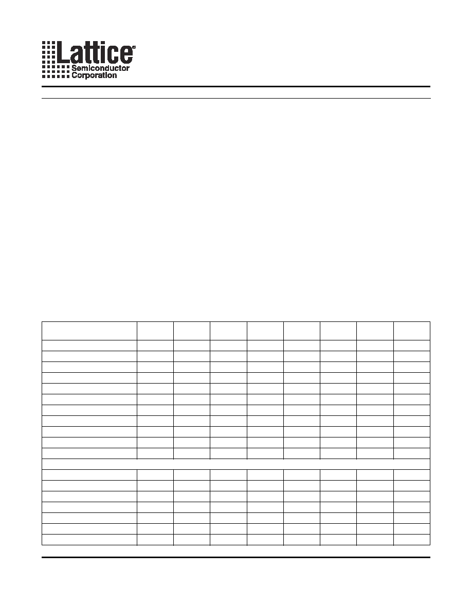
Table 1-1. LatticeECP/EC Family Selection Guide
Device LFEC1
LFEC3
LFEC6/
LFECP6
LFEC10/
LFECP10
LFEC15/
LFECP15
LFEC20/
LFECP20
LFEC33/
LFECP33
LFEC40/
LFECP40
PFU/PFF Rows
12
16
24
32
40
44
64
64
PFU/PFF Columns
16
24
32
40
48
56
64
80
PFUs/PFFs
192
384
768
1280
1920
2464
4096
5120
LUTs (K)
1.5
3.1
6.1
10.2
15.4
19.7
32.8
41.0
Distributed RAM (Kbits)
6
12
25
41
61
79
131
164
EBR SRAM (Kbits)
18
55
92
277
350
424
535
645
EBR SRAM Blocks
2
6
10
30
38
46
58
70
sysDSP Blocks
1
--
--
4
5
6
7
8
10
18x18 Multipliers
1
--
--
16
20
24
28
32
40
V
CC
Voltage (V)
1.2
1.2
1.2
1.2
1.2
1.2
1.2
1.2
Number of PLLs
2
2
2
4
4
4
4
4
Packages and I/O Combinations:
100-pin TQFP (14 x 14 mm)
67
67
144-pin TQFP (20 x 20 mm)
97
97
97
208-pin PQFP (28 x 28 mm)
112
145
147
147
256-ball fpBGA (17 x 17 mm)
160
195
195
195
484-ball fpBGA (23 x 23 mm)
224
288
352
360
360
672-ball fpBGA (27 x 27 mm)
400
496
496
900-ball fpBGA (31 x 31 mm)
576
1. LatticeECP devices only.
LatticeECP/EC Family Data Sheet
Introduction

1-2
Introduction
Lattice Semiconductor
LatticeECP/EC Family Data Sheet
Introduction
The LatticeECP/EC family of FPGA devices has been optimized to deliver mainstream FPGA features at low cost.
For maximum performance and value, the LatticeECP (EConomy Plus) FPGA concept combines an efficient FPGA
fabric with high-speed dedicated functions. Lattice's first family to implement this approach is the LatticeECP-DSP
(EConomy Plus DSP) family, providing dedicated high-performance DSP blocks on-chip. The LatticeECTM (ECon-
omy) family supports all the general purpose features of LatticeECP devices without dedicated function blocks to
achieve lower cost solutions.
The LatticeECP/EC FPGA fabric, which was designed from the outset with low cost in mind, contains all the critical
FPGA elements: LUT-based logic, distributed and embedded memory, PLLs and support for mainstream I/Os.
Dedicated DDR memory interface logic is also included to support this memory that is becoming increasingly prev-
alent in cost-sensitive applications.
The ispLEVER
�
design tool from Lattice allows large complex designs to be efficiently implemented using the Latti-
ceECP/EC family of FPGA devices. Synthesis library support for LatticeECP/EC is available for popular logic syn-
thesis tools. The ispLEVER tool uses the synthesis tool output along with the constraints from its floor planning
tools to place and route the design in the LatticeECP/EC device. The ispLEVER tool extracts the timing from the
routing and back-annotates it into the design for timing verification.
Lattice provides many pre-designed IP (Intellectual Property) ispLeverCORETM modules for the LatticeECP/EC
family. By using these IPs as standardized blocks, designers are free to concentrate on the unique aspects of their
design, increasing their productivity.

www.latticesemi.com
2-1
Architecture_01.3
November 2004
Preliminary Data Sheet
� 2004 Lattice Semiconductor Corp. All Lattice trademarks, registered trademarks, patents, and disclaimers are as listed at www.latticesemi.com/legal. All other brand
or product names are trademarks or registered trademarks of their respective holders. The specifications and information herein are subject to change without notice.
Architecture Overview
The LatticeECPTM-DSP and LatticeECTM architectures contain an array of logic blocks surrounded by Programma-
ble I/O Cells (PIC). Interspersed between the rows of logic blocks are rows of sysMEM Embedded Block RAM
(EBR) as shown in Figures 2-1 and 2-2. In addition, LatticeECP-DSP supports an additional row of DSP blocks as
shown in Figure 2-2.
There are two kinds of logic blocks, the Programmable Functional Unit (PFU) and Programmable Functional unit
without RAM/ROM (PFF). The PFU contains the building blocks for logic, arithmetic, RAM, ROM and register func-
tions. The PFF block contains building blocks for logic, arithmetic and ROM functions. Both PFU and PFF blocks
are optimized for flexibility allowing complex designs to be implemented quickly and efficiently. Logic Blocks are
arranged in a two-dimensional array. Only one type of block is used per row. The PFU blocks are used on the out-
side rows. The rest of the core consists of rows of PFF blocks interspersed with rows of PFU blocks. For every
three rows of PFF blocks there is a row of PFU blocks.
Each PIC block encompasses two PIOs (PIO pairs) with their respective sysIO interfaces. PIO pairs on the left and
right edges of the device can be configured as LVDS transmit/receive pairs. sysMEM EBRs are large dedicated fast
memory blocks. They can be configured as RAM or ROM.
The PFU, PFF, PIC and EBR Blocks are arranged in a two-dimensional grid with rows and columns as shown in
Figure 2-1. The blocks are connected with many vertical and horizontal routing channel resources. The place and
route software tool automatically allocates these routing resources.
At the end of the rows containing the sysMEM Blocks are the sysCLOCK Phase Locked Loop (PLL) Blocks. These
PLLs have multiply, divide and phase shifting capability; they are used to manage the phase relationship of the
clocks. The LatticeECP/EC architecture provides up to four PLLs per device.
Every device in the family has a JTAG Port with internal Logic Analyzer (ispTRACY) capability. The sysCONFIGTM
port which allows for serial or parallel device configuration. The LatticeECP/EC devices use 1.2V as their core volt-
age.
LatticeECP/EC Family Data Sheet
Architecture

2-2
Architecture
Lattice Semiconductor
LatticeECP/EC Family Data Sheet
Figure 2-1. Simplified Block Diagram, LatticeECP/EC Device (Top Level)
Figure 2-2. Simplified Block Diagram, LatticeECP-DSP Device (Top Level)
Programmable I/O Cell
(PIC) includes sysIO
Interface
sysCONFIG Programming
Port (includes dedicated
and dual use pins)
Programmable
Functional Unit (PFU)
sysCLOCK PLL
PFF (PFU without
RAM)
JTAG Port
sysMEM Embedded
Block RAM (EBR)
Programmable I/O Cell
(PIC) includes sysIO
Interface
sysCONFIG Programming
Port (includes dedicated
and dual use pins)
Programmable
Functional Unit (PFU)
sysDSP Block
sysCLOCK PLL
PFF (Fast PFU
without RAM/ROM)
JTAG Port
sysMEM Embedded
Block RAM (EBR)
