www.latticesemi.com
1
ip1030_01
May 2004
IP Data Sheet
© 2004 Lattice Semiconductor Corp. All Lattice trademarks, registered trademarks, patents, and disclaimers are as listed at www.latticesemi.com/legal. All other brand
or product names are trademarks or registered trademarks of their respective holders. The specifications and information herein are subject to change without notice.
The product described herein is subject to continuing development, and applicable specifications and information are subject to change without notice. Such specifica-
tions and information are provided in good faith; actual performance is not guaranteed, as it is dependent on many factors, including the user's system design.
1GbE PCS IP Core
Features
Complete 1Gb Ethernet Physical Coding
Sublayer Solution Based on the ORCA
Æ
ORT42G5 Device
IP Targeted to the ORT42G5 Programmable
Array Section Implements Functionality
Conforming to IEEE 803.2-2002
≠ Encoding/decoding for GMII data octets
≠ Optional Auto-negotiation function with manage-
ment registers and interface
≠ External GMII interface or internal interface to
single chip MAC and PCS implementation
Ethernet Functionality Supported by the
Embedded Section of the ORT42G5,
Including:
≠ Support for 8b/10b encoding/decoding
≠ Serialization/deserialization of code groups for
transmit/receive
≠ Clock recovery from encoded data stream
Simulation Models and Test Benches
Available for Free Evaluation
General Description
The GbE PCS Intellectual Property (IP) Core targets
the programmable array section of the ORCA
ORT42G5
FPSC and provides the PCS (Physical Coding Sub-
layer) function.
The ORT42G5 device is built on the Series 4 re-config-
urable embedded System-on-a-Chip (SoC) architec-
ture and is made up of SERDES transceivers containing
four channels, each operating at up to 3.7Gbps, with a
full-duplex synchronous interface with built-in RX Clock
and Data Recovery (CDR), and transmitter pre-empha-
sis, for high-speed data transmission.
PCS (Physical Coding Sublayer) and PMA (Physical
Media Attachment) are sublayers of the physical layer
implementation of IEEE 802.3 standards. The PCS pro-
vides a uniform interface to the MAC sublayer through
GMII (Gigabit Media Independent Interface) for all
1000Mb/s PHY implementations. The 1GbE PCS IP
core is provided with implementation scripts, test
benches and documentation.
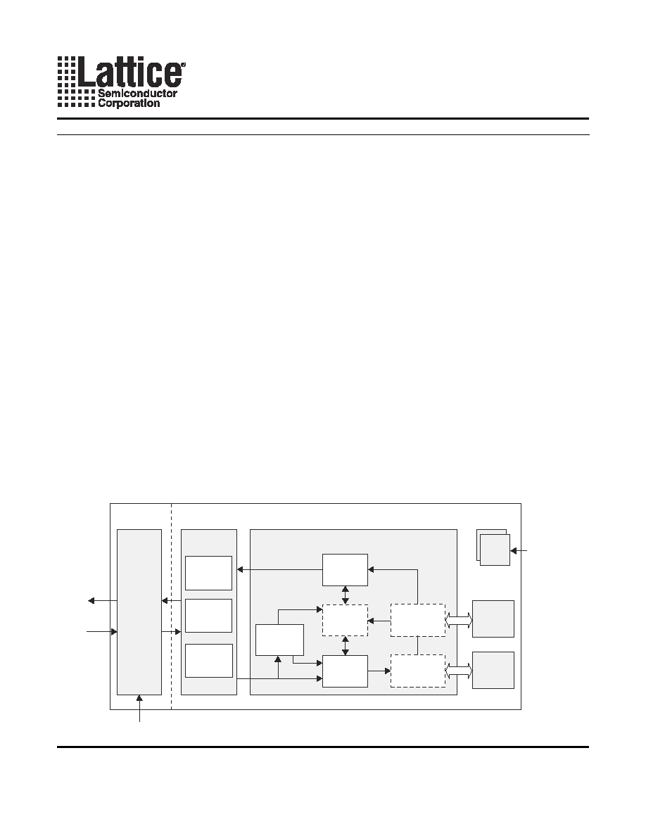
Block Diagram
Figure 1. 1GbE PCS Solution
tx_sm
Optional
autoneg
tx_sync
Embedded
ASB Section
ORT42G5 Device
Programmable Array Section
1G Line
umi
rx_sync_cc
rx_sm
ort42g5_inf
rx_sync_sm
rx_sync_sm
Optional
gmii_mac_inf
Optional
Management
Interface
pcs_1g_core
GMII or
MAC
Interface
PLL
MDIO
or MAC
interface
125MHz
tx/rx
clocks
PLL
SERDES
8b/10b
Systembus
of
ORT42G5
(ASB)
Note: Optional interfaces are not needed if an Ethernet MAC Interfafce is present on-chip

Lattice Semiconductor
1GbE PCS IP Core
2
Functional Description
The major blocks in the GbE PCS core are shown in Figure 1. Descriptions of these blocks follow.
Transmit Section
This section implements the Transmit State Machine which is specified by Figures 36-5 and 36-6 in Clause 36 of
the IEEE 802.3-2002 Standard.
The PCS Transmit process continuously generates code groups based upon the
TXD <7:0>
,
TX_EN
and
TX_ER
signals on the GMII, sending them immediately to the Line Interface. The PCS Transmit process monitors the Auto-
negotiation process transmit flag to determine whether to transmit data or reconfigure the link.
Receive Section
Receive Synchronization State Machine
This module implements the synchronization state machine which is specified by Figure 36-9 of the IEEE 802.3-
2002 Standard.
The Synchronization process is responsible for determining whether the underlying receive channel is ready for
operation. The process continuously accepts code groups from the Line Interface and scans them to detect the
acquisition and maintenance of code group synchronization. This state machine also sets the
sync_status
flag
which is monitored by the receive state machine.
Receive State Machine
This module implements the receive state machine, which is specified by Figures 36-7a and 36-7b in Clause 36 of
the IEEE 802.3-2002 Standard.
The PCS Receive process continuously accepts and monitors code-groups from the Line Interface and generates
RXD <7:0>
,
RX_DV
and
RX_ER
on the GMII, and the internal receiving flag used by the Carrier Sense and Trans-
mit processes.
Auto-negotiation
This module implements the auto-negotiation state machine, which is specified by the Figure 37-6 in Clause 37 of
the IEEE 802.3-2002 Standard.
The Auto-negotiation function that allows a device (local device) to advertise modes of operation it possesses to a
device at the remote end of a link segment (link partner) and to detect corresponding operational modes that the
link partner may be advertising. The Auto-negotiation function exchanges information between two devices that
share a link segment and automatically configures both devices to take maximum advantage of their abilities.
Management Interface
The MDIO Management Interface is implemented based on specifications in Clause 22 of the IEEE 802.3-2002
Standard.
The management interface is used to connect a management entity and a managed PHY for the purposes of con-
trolling the PHY and gathering status from the PHY. The management interface consists of a pair of signals that
physically transport the management information across the GMII, a frame format and a protocol specification for
exchanging management frames, and a register set that can be read and written using these frames.
GMII Interface
This module, depending on the configuration, provides a GMII Interface or a connection to an on-chip MAC.

Lattice Semiconductor
1GbE PCS IP Core
3
ORT42G5 Interface
This section provides the following functions:
∑ A bridging function between the 8-bit PCS core and the 32-bit Application Specific Block (ASB). The data
rate translation cross the two clock domains is achieved using asynchronous FIFOs.
∑ Clock compensation to a tolerance of +/- 100ppm between the recovered clock and IP system clock. This is
done by insertion or deletion of idle characters.
∑ Logic to program the control registers inside the ASB through the system bus User Master Interface.
Design Parameters
Table 1. Parameter Descriptions
Signal Descriptions
Parameter
Description
GMII_INF
If this parameter is set to "yes", a GMII interface will be provided through the
FPGA I/Os to an external device. If this parameter is set to "no", an internal
interface will be provided to a MAC on the same chip.
AUTO_NEG
If this parameter is set to "yes", the Auto-negotiation module and Manage-
ment registers will be enabled. If this parameter is set to "no", the Auto-
negotiation module and Management registers will be disabled.
MDIO_INF
The optional MDIO Interface is only available if the Auto-negotiation param-
eter is set to "yes". If the MDIO parameter is set to "yes", an MDIO interface
will be provided through the FPGA I/Os to an external device.
Table 2. Signal Definitions for GbE PCS Solution I/O
Signal Name
Direction
Description
Clocks and Resets
RX_CLK_125
Input
Receive Clock (125MHz)
TX_CLK_125
Input
Transmit Clock (125MHz)
RST_N
Input
Active Low Reset
USR_CLK
Input
Clock for the User Master Interface
GMII/MAC Interface
RX_DV
Output
Receive Data Valid
RX_D [7:0]
Output
Receive Data Bus
RX_ER
Output
Receive
TX_ER
Input
Transmit Error Indicator
TX_D [7:0]
Input
Transmit Data Bus
TX_DV
Input
Transmit Data Valid
MDIO Signals
MDC
Input
MDIO clock
MDIO
Input/Output
MDIO bi-directional data
Line Interface
1
REFCLKN_A
Input
CML reference clock input ≠ SERDES Quad A
REFCLKP_A
Input
CML reference clock input ≠ SERDES Quad A
HDINN_AC
Input
High-speed CML receive data input ≠ SERDES Quad A, Channel C
HDINP_AC
Input
High-speed CML receive data input ≠ SERDES Quad A, Channel C
HDOUTN_AC
Output
High-speed CML receive data output ≠ SERDES Quad A, Channel C
HDOUTP_AC
Output
High-speed CML receive data output ≠ SERDES Quad A, Channel C

Lattice Semiconductor
1GbE PCS IP Core
4
Table 3. Signal Definitions for GbE PCS Solution ≠ FPGA/Embedded ASB Interface (Internal to ORT42G5
Device)
1
Auto-negotiation Signals
(if MDIO is not implemented)
MR_ADV_ABILITY[
15:0]
Input
Advertisement Register
MR_AN_ENABLE
Input
Enable Auto-negotiation
MR_RESTART_EN
Input
Restart Auto-negotiation
MR_AN_COMPLETE
Output
Auto-negotiation Complete
MR_LP_ADV_ABILI
TY[15:0]
Output
Link Partner Ability Register
MR_PAGE_RX
Output
Page Received
LINK_STATUS
Output
Link Status
Control Signals
(if MDIO is not implemented)
MR_MAIN_RESET
Input
Core Reset
MR_LOOPBACK
Input
Enable Loopback
1. The signals listed here are required for the Embedded SPI-4 interface Quad A, Channel C. Please refer to the ORT42G5 Data Sheet for
additional information on configuring the SPI-4 interface for specific applications.
Signal Name
FPGA
Direction
Description
Receive Interface Signals
RSYSCLK_A2
Output
Low-speed receive FIFO clock for Channel AC
RCK78A
Input
Receive low-speed clock to FPGA ≠ SERDES Quad A
MRWDAC[39]
Input
Code violation for Receive Data Byte 3 Channel AC
MRWDAC[38]
Input
K_CTRL for Receive Data Byte 3 Channel AC
MRWDAC[37:30]
Input
Receive Data Byte 3 Channel AC
MRWDAC[29]
Input
Code violation for Receive Data Byte 2 Channel AC
MRWDAC[28]
Input
K_CTRL for Receive Data Byte 2 Channel AC
MRWDAC[27:20]
Input
Receive Data Byte 2 Channel AC
MRWDAC[19]
Input
Code violation for Receive Data Byte 1 Channel AC
MRWDAC[18]
Input
K_CTRL for Receive Data Byte 1 Channel AC
MRWDAC[17:10]
Input
Receive Data Byte 1 Channel AC
MRWDAC[9]
Input
Code violation for Receive Data Byte 0 Channel AC
MRWDAC[8]
Input
K_CTRL for Receive Data Byte 0 Channel AC
MRWDAC[7:0]
Input
Receive Data Byte 0 Channel AC
Transmit Interface Signals
TSYSCLK_AC
Output
Transmit Low Speed Clock Channel AC
TCK78A
Input
Transmit Low Speed Clock to FPGA ≠ SERDES Quad A
TWDAC[31:0]
Output
Transmit Data Channel AC
TCOMMAAC[3:0]
Output
Transmit Comma Character Channel AC
TBIT9AC[3:0]
Output
Transmit Force Negative Disparity Channel AC
1. The signals listed here are required for the Embedded SPI-4 interface Quad A, Channel C. Please refer to the ORT42G5 Data Sheet for
additional information on configuring the SPI-4 interface for specific applications.
Table 2. Signal Definitions for GbE PCS Solution I/O (Continued)
Signal Name
Direction
Description

Lattice Semiconductor
1GbE PCS IP Core
5
Custom Core Configurations
To request features or a custom 1GbE PCS core configuration, please contact your Lattice sales office.
Related Information
For more information regarding core usage and design verification, refer to the
1GbE PCS Core User's Guide,
available on the Lattice web site at www.latticesemi.com.

Lattice Semiconductor
1GbE PCS IP Core
6
Appendix for ORCA Series 4 ORT42G5 FPSC
Table 4. Available Configuration
Table 5. Performance and Utilization
1
Supplied Netlist Configurations
The Ordering Part Number (OPN) for all configurations of this core is 1GBE-PCS-O4-N1.
To load the preset parameters for this core, click on the "Load Parameters" button inside the IP Manager tool. Make
sure that you are looking for a file inside of this core's directory location. The Lattice Parameter Configuration files
(.lpc) are located inside this directory.
Configuration
Number
Configuration Features
001
∑ GMII interface through FPGA I/Os.
∑ No auto-negotiation and Management registers.
∑ No MDIO interface.
Configuration
PFUs
Block RAM
PLL
LUTs
Registers
f
MAX
1gbe_pcs_o4_1_001
157
4
2
622
605
125 MHz
tx_clk
rx_clk
1. Performance and utilization characteristics are generated using an ORT42G5-2BM484C in Lattice's ispLEVER
Æ
v.4.0 software. When using
this IP core in a different density, package, speed, or grade within the ORT42G5 family, performance may vary.