
Preliminary Data Sheet
April 2002
ORCA
ģ
ORT4622 Field-Programmable System Chip (FPSC)
Four-Channel x 622 Mbits/s Backplane Transceiver
Introduction
Lattice has developed a solution for designers who
need the many advantages of FPGA-based design
implementation, coupled with high-speed serial back-
plane data transfer. The 622 Mbits/s backplane trans-
ceiver offers a clockless, high-speed interface for
interdevice communication on a board or across a
backplane. The built-in clock recovery of the
ORT4622 allows for higher system performance,
easier-to-design clock domains in a multiboard sys-
tem, and fewer signals on the backplane. Network
designers will benefit from the backplane transceiver
as a network termination device. The backplane
transceiver offers SONET scrambling/descrambling
of data and streamlined SONET framing, pointer
moving, and transport overhead handling, plus the
programmable logic to terminate the network into
proprietary systems. For non-SONET applications,
all SONET functionality is hidden from the user and
no prior networking knowledge is required.
Embedded Core Features
Implemented in an
ORCA
Series 3 FPGA array.
Allows wide range of applications for SONET net-
work termination application as well as generic data
moving for high-speed backplane data transfer.
No knowledge of SONET/SDH needed in generic
applications. Simply supply data, 78 MHz clock, and
a frame pulse.
High-speed interface (HSI) function for clock/data
recovery serial backplane data transfer without
external clocks.
HSI function uses Lattice's proven 622 Mbits/s
serial interface core.
Four-channel HSI function provides 622 Mbits/s
serial interface per channel for a total chip band-
width of 2.5 Gbits/s (full duplex).
LVDS I/Os compliant with
EIA
*-644, support hot
insertion.
8:1 data multiplexing/demultiplexing for 77.76 MHz
byte-wide data processing in FPGA logic.
On-chip phase-lock loop (PLL) clock meets B jitter
tolerance specification of ITU-T Recommendation
G.958 (0.6
UI
P-P
at 250 kHz).
Powerdown option of HSI receiver on a per-
channel basis.
Highly efficient implementation with only 3% over-
head vs. 25% for 8B10B coding.
In-Band management and configuration.
Streamlined pointer processor (pointer mover) for
8 kHz frame alignment to system clocks.
Built-in boundry scan (
IEEE
1149.1 JTAG).
FIFOs align incoming data across all four channels
for STS-48 (2.5 Gbits/s) operation (in quad STS-12
format).
1 + 1 protection supports STS-12/STS-48 redun-
dancy by either software or hardware control for
protection switching applications.
*
EIA
is a registered trademark of Electronic Industries Associa-
tion.
IEEE
is a registered trademark of The Institute of Electrical and
Electronics Engineers, Inc.
Table 1.
ORCA
ORT4622--Available FPGA Logic
The embedded core and interface are not included in the above gate counts. The usable gate count range from a logic-only gate count to
a gate count assuming 30% of the PFUs/SLICs being used as RAMs. The logic-only gate count includes each PFU/SLIC (counted as
108 gates per PFU/SLIC), including 12 gates pre-LUT/FF pair (eight per PFU), and 12 gates per SLC/FF pair (one per PFU). Each of the
four PIOs per PIC is counted as 16 gates (two FFs, fast-capture latch, output logic, CLK drivers, and I/O buffers). PFUs used as RAM are
counted at four gates per bit, with each PFU capable of implementing a 32 x 4 RAM (or 512 gates) per PFU.
Device
Usable
System
Gates
Number of
LUTs
Number of
Registers
Max User
RAM
Max User
I/Os
Array Size
Number of
PFUs
ORT4622
60K--120K
4032
5304
64K
259
18 x 28
504

Table of Contents
Contents
Page
Contents
Page
ORCA
ORT4622 FPSC
Preliminary Data Sheet
Four-Channel x 622 Mbits/s Backplane Transceiver
April 2002
Lattice Semiconductor
2
Introduction ............................................................... 1
Embedded Core Features ........................................ 1
FPSC Highlights ........................................................ 3
Software Support ....................................................... 3
Description ................................................................ 4
What Is an FPSC? ............................................... 4
FPSC Overview ................................................... 4
FPSC Gate Counting .......................................... 4
FPGA/Embedded Core Interface ....................... 4
ORCA
Foundry
Development System ............. 4
FPSC Design Kit ................................................. 5
FPGA Logic Overview ........................................ 5
PLC Logic ............................................................ 5
PIC Logic ............................................................ 6
System Features ................................................. 6
Routing ............................................................... 6
Configuration ...................................................... 6
More Series 3 Information .................................. 6
ORT4622 Overview ................................................... 7
Device Layout ..................................................... 7
Backplane Transceiver Interface ....................... 7
HSI Interface ....................................................... 9
STM Macrocell .................................................... 9
CPU Interface ..................................................... 9
FPGA Interface ................................................... 9
FPSC Configuration ............................................ 11
Generic Backplane Transceiver
Application ............................................................... 11
Backplane Transceiver Core Detailed Description ... 12
HSI Macro ........................................................... 12
STM Transmitter (FPGA -> Backplane) .............. 14
STM Receiver (Backplane -> FPGA) .................. 18
Powerdown Mode ............................................... 24
Redundancy and Protection Switching .............. 24
Memory Map ............................................................. 25
Definition of Register Types ............................... 25
Memory Map Overview ...................................... 26
Powerup Sequencing for ORT4622 Device .............. 34
FPGA Configuration Data Format ............................. 35
Using ORCA Foundry to Generate Configuration
RAM Data ......................................................... 35
FPGA Configuration Data Frame ........................ 35
Bit Stream Error Checking ........................................ 37
FPGA Configuration Modes ...................................... 37
Absolute Maximum Ratings ...................................... 38
Recommend Operating Conditions .......................... 38
Electrical Characteristics .......................................... 39
HSI Circuit Specifications ......................................... 40
Input Data ........................................................... 40
Jitter Tolerance ................................................... 40
Generated Output Jitter ...................................... 40
PLL ..................................................................... 40
Input Reference Clock ........................................ 40
Power Supply Decoupling LC Circuit ................. 41
LVDS I/O .................................................................... 42
LVDS Receiver Buffer Requirements .................. 43
Timing Characteristics .............................................. 44
Description ......................................................... 44
PFU Timing ......................................................... 45
PLC Timing ......................................................... 45
SLIC Timing ........................................................ 45
PIO Timing .......................................................... 45
Special Function Timing ..................................... 45
Clock Timing ....................................................... 45
Configuration Timing .......................................... 45
Readback Timing ............................................... 45
Input/Output Buffer Measurement Conditions
(on-LVDS Buffer) ...................................................... 55
FPGA Output Buffer Characteristics ......................... 56
LVDS Buffer Characteristics ...................................... 57
Termination Resistor ........................................... 57
LVDS Driver Buffer Capabilities .......................... 57
Estimating Power Dissipation .................................... 58
ORT4622 Clock Power ....................................... 58
Pin Information .......................................................... 59
Package Thermal Characteristics Summary ............. 82
JA ................................................................... 82
JC ..................................................................... 82
JC ................................................................... 82
JB ................................................................... 82
FPGA Maximum Junction Temperature .............. 82
Package Thermal Characteristics ............................. 83
Package Coplanarity ................................................. 83
Package Parasitics .................................................... 83
Package Outline Diagrams ....................................... 85
Terms and Definitions ......................................... 85
432-Pin EBGA ..................................................... 86
680-Pin PBGAM .................................................. 87
Ordering Information ................................................. 88

ORCA
ORT4622 FPSC
Preliminary Data Sheet
Four-Channel x 622 Mbits/s Backplane Transceiver
April 2002
3
Lattice Semiconductor
Embedded Core Features
(continued)
Pseudo-SONET protocol including A1/A2 framing.
SONET scrambling and descrambling for required
ones density (optional).
Selected transport overhead (TOH) bytes insertion
and extraction for interdevice communication via the
TOH serial link.
FPSC Highlights
Implemented as an embedded core in the
ORCA
Series 3+ FPSC architecture.
Allows the user to integrate the core with up to 120K
gates of programmable logic (all in one device) and
provides up to 242 user I/Os in addition to the
embedded core I/O pins.
FPGA portion retains all of the features of the
ORCA
Series 3 FPGA architecture:
-- High-performance, cost-effective, 0.25 Ķm, 5-level
metal technology.
-- Twin-quad programmable function unit (PFU)
architecture with eight 16-bit look-up tables
(LUTs) per PFU, organized in two nibbles for use
in nibble- or byte-wide functions. Allows for mixed
arithmetic and logic functions in a single PFU.
-- Softwired LUTs (SWL) allow fast cascading of up
to three levels of LUT logic in a single PFU.
-- Supplemental logic and interconnect cell (SLIC)
provides 3-statable buffers, up to 10-bit decoder,
and
PAL
*-like AND-OR-INVERT (AOI) in each
programmable logic cell (PLC).
-- Up to three ExpressCLK inputs allow extremely
fast clocking of signals on- and off-chip plus
access to internal general clock routing.
-- Dual-use microprocessor interface (MPI) can be
used for configuration, as well as for a general-
purpose interface to the FPGA. Glueless interface
to
i960
and
PowerPC
processors with user-
configurable address space provided.
-- Programmable clock manager (PCM) adjusts
clock phase and duty cycle for input clock rates
from 5 MHz to 120 MHz. The PCM may be com-
bined with FPGA logic to create complex
functions, such as digital phase-locked loops,
frequency counters, and frequency synthesizers
or clock doublers. Two PCMs are provided per
device.
-- True internal 3-state, bidirectional buses with
simple control provided by the SLIC.
-- 32 x 4 RAM per PFU, configurable as single or
dual port. Create large, fast RAM/ROM blocks
(128 x 8 in only eight PFUs) using the SLIC
decoders as bank drivers.
-- Built-in boundary scan (
IEEE
1149.1 JTAG) and
TS_ALL testability function to 3-state all I/O pins.
High-speed, on-chip interface provided between
FPGA logic and embedded core to reduce bottle-
necks typically found when interfacing off-chip.
Software Support
Supported by
ORCA
Foundry software and third-
party CAE tools for implementing
ORCA
Series 3+
devices and simulation/timing analysis with the
embedded core functions.
Embedded core configuration options and simulation
netlists generated by FPSC Configuration Manager
utility.
*
PAL
is a trademark of Advanced Micro Devices, Inc.
i960
is a registered trademark of Intel Corporation.
PowerPC
is a registered trademark of International Business
Machines Corporation.

Lattice Semiconductor
4
Preliminary Data Sheet
ORCA
ORT4622 FPSC
April 2002
Four-Channel x 622 Mbits/s Backplane Transceiver
Description
What Is an FPSC?
FPSCs, or field-programmable system chips, are
devices that combine field-programmable logic with
ASIC or mask-programmed logic on a single device.
FPSCs provide the time to market and flexibility of
FPGAs, the design effort savings of using soft intellec-
tual property (IP) cores, and the speed, design density,
and economy of ASICs.
FPSC Overview
Lattice's Series 3+ FPSCs are created from Series 3
ORCA
FPGAs. To create a Series 3+ FPSC, several
rows of programmable logic cells (see FPGA Logic
Overview section for FPGA logic details) are removed
from a Series 3
ORCA
FPGA, and the area is replaced
with an embedded logic core. Other than replacing
some FPGA gates with ASIC gates, at greater than
10:1 efficiency, none of the FPGA functionality is
changed--all of the Series 3 FPGA capability is
retained: MPI, PCMs, boundary scan, etc. The rows of
programmable logic are replaced at the bottom of the
device, allowing pins on the bottom and sides of the
replaced rows to be used as I/O pins for the embedded
core. The remainder of the device pins retain their
FPGA functionality as do special function FPGA pins
within the embedded core area.
FPSC Gate Counting
The total gate count for an FPSC is the sum of its
embedded core (standard-cell/ASIC gates) and its
FPGA gates. Because FPGA gates are generally
expressed as a usable range with a nominal value, the
total FPSC gate count is sometimes expressed in the
same manner. Standard-cell ASIC gates are, however,
10 to 25 times more silicon area efficient than FPGA
gates. Therefore, an FPSC with an embedded function
is gate equivalent to an FPGA with a much larger gate
count.
FPGA/Embedded Core Interface
The interface between the FPGA logic and the embed-
ded core is designed to look like FPGA I/Os from the
FPGA side, simplifying interface signal routing and pro-
viding a unified approach with general FPGA design.
Effectively, the FPGA is designed as if signals were
going off of the device to the embedded core, but the
on-chip interface is much faster than going off-chip and
requires less power. All of the delays for the interface
are precharacterized and accounted for in the
ORCA
Foundry Development System.
Clock spines also can pass across the FPGA/embed-
ded core boundary. This allows for fast, low-skew clock-
ing between the FPGA and the embedded core. Many
of the special signals from the FPGA, such as DONE
and global set/reset, are also available to the embed-
ded core, making it possible to fully integrate the
embedded core with the FPGA as a system.
For even greater system flexibility, FPGA configuration
RAMs are available for use by the embedded core. This
allows for user-programmable options in the embedded
core, in turn allowing for greater flexibility. Multiple
embedded core configurations may be designed into a
single device with user-programmable control over
which configurations are implemented, as well as the
capability to change core functionality simply by recon-
figuring the device.
ORCA
Foundry Development System
The
ORCA
Foundry Development System is used to
process a design from a netlist to a configured FPSC.
This system is used to map a design onto the
ORCA
architecture and then place and route it using
ORCA
Foundry's timing-driven tools. The development system
also includes interfaces to, and libraries for, other popu-
lar CAE tools for design entry, synthesis, simulation,
and timing analysis.
The
ORCA
Foundry Development System interfaces to
front-end design entry tools and provides the tools to
produce a configured FPSC. In the design flow, the
user defines the functionality of the FPGA portion of
the FPSC and embedded core settings at two points in
the design flow: at design entry and at the bit stream
generation stage. Following design entry, the develop-
ment system's map, place, and route tools translate the
netlist into a routed FPSC. A static timing analysis tool
is provided to determine device speed, and a back-
annotated netlist can be created to allow simulation.

ORCA
ORT4622 FPSC
Preliminary Data Sheet
Four-Channel x 622 Mbits/s Backplane Transceiver
April 2002
5
Lattice Semiconductor
Description
(continued)
Timing and simulation output files from
ORCA
Foundry
are also compatible with many third-party analysis
tools. Its bit stream generator is then used to generate
the configuration data which is loaded into the FPSC's
internal configuration RAM.
When using the bit stream generator, the user selects
options that affect the functionality of the FPSC. Com-
bined with the front-end tools,
ORCA
Foundry pro-
duces configuration data that implements the various
logic and routing options discussed in this data sheet.
FPSC Design Kit
Development is facilitated by an FPSC design kit
which, together with
ORCA
Foundry and third-party
synthesis and simulation engines, provides all software
and documentation required to design and verify an
FPSC implementation. Included in the kit are the FPSC
configuration manager, HDL gate-level structural
netlists, all necessary synthesis libraries, and complete
online documentation. The kit's software couples with
ORCA
Foundry, providing a seamless FPSC design
environment. More information can be obtained by vis-
iting the
ORCA
website or contacting a local sales
office, both listed on the last page of this document.
FPGA Logic Overview
ORCA
Series 3 FPGA logic is a new generation of
SRAM-based FPGA logic built on the successful
Series 2 FPGA line, with enhancements and innova-
tions geared toward today's high-speed designs on a
single chip. Designed from the start to be synthesis
friendly and to reduce place and route times while
maintaining the complete routability of the
ORCA
Series 2 devices, the Series 3 more than doubles the
logic available in each logic block and incorporates sys-
tem-level features that can further reduce logic require-
ments and increase system speed.
ORCA
Series 3
devices contain many new patented enhancements
and are offered in a variety of packages, speed grades,
and temperature ranges.
ORCA
Series 3 FPGA logic consists of three basic ele-
ments: programmable logic cells (PLCs), programma-
ble input/output cells (PICs), and system-level features.
An array of PLCs is surrounded by PICs. Each PLC
contains a programmable function unit (PFU), a sup-
plemental logic and interconnect cell (SLIC), local rout-
ing resources, and configuration RAM. Most of the
FPGA logic is performed in the PFU, but decoders,
PAL
-like functions, and 3-state buffering can be per-
formed in the SLIC. The PICs provide device inputs and
outputs and can be used to register signals and to per-
form input demultiplexing, output multiplexing, and
other functions on two output signals. Some of the sys-
tem-level functions include the new microprocessor
interface (
MPI
) and the programmable clock manager
(
PCM
).
PLC Logic
Each PFU within a PLC contains eight 4-input (16-bit)
look-up tables (LUTs), eight latches/flip-flops (FFs),
and one additional flip-flop that may be used indepen-
dently or with arithmetic functions.
The PFU is organized in a twin-quad fashion: two sets
of four LUTs and FFs that can be controlled indepen-
dently. LUTs may also be combined for use in arith-
metic functions using fast-carry chain logic in either
4-bit or 8-bit modes. The carry-out of either mode may
be registered in the ninth FF for pipelining. Each PFU
may also be configured as a synchronous 32 x 4
single- or dual-port RAM or ROM. The FFs (or latches)
may obtain input from LUT outputs or directly from
invertible PFU inputs, or they can be tied high or tied
low. The FFs also have programmable clock polarity,
clock enables, and local set/reset.
The SLIC is connected to PLC routing resources and to
the outputs of the PFU. It contains 3-state, bidirectional
buffers and logic to perform up to a 10-bit AND function
for decoding, or an AND-OR with optional INVERT
(AOI) to perform
PAL
-like functions. The 3-state drivers
in the SLIC and their direct connections to the PFU out-
puts make fast, true 3-state buses possible within the
FPGA logic, reducing required routing and allowing for
real-world system performance.

Lattice Semiconductor
6
Preliminary Data Sheet
ORCA
ORT4622 FPSC
April 2002
Four-Channel x 622 Mbits/s Backplane Transceiver
Description
(continued)
PIC Logic
The Series 3 PIC addresses the demand for ever-
increasing system clock speeds. Each PIC contains
four programmable inputs/outputs (PIOs) and routing
resources. On the input side, each PIO contains a fast-
capture latch that is clocked by an
ExpressCLK
. This
latch is followed by a latch/FF that is clocked by a sys-
tem clock from the internal general clock routing. The
combination provides for very low setup requirements
and zero hold times for signals coming on-chip. It may
also be used to demultiplex an input signal, such as a
multiplexed address/data signal, and register the sig-
nals without explicitly building a demultiplexer. Two
input signals are available to the PLC array from each
PIO, and the
ORCA
Series 2 capability to use any input
pin as a clock or other global input is maintained.
On the output side of each PIO, two outputs from the
PLC array can be routed to each output flip-flop, and
logic can be associated with each I/O pad. The output
logic associated with each pad allows for multiplexing
of output signals and other functions of two output sig-
nals.
The output FF, in combination with output signal multi-
plexing, is particularly useful for registering address
signals to be multiplexed with data, allowing a full clock
cycle for the data to propagate to the output. The I/O
buffer associated with each pad is the same as the
ORCA
Series 3 buffer.
System Features
The Series 3 also provides system-level functionality
by means of its dual-use microprocessor interface
(MPI) and its innovative programmable clock manager
(PCM). These functional blocks allow for easy glueless
system interfacing and the capability to adjust to vary-
ing conditions in today's high-speed systems. Since
these and all other Series 3 features are available in
every Series 3+ FPSC, they can also interface to the
embedded core providing for easier system integration.
Routing
The abundant routing resources of
ORCA
Series 3
FPGA logic are organized to route signals individually
or as buses with related control signals. Clocks are
routed on a low-skew, high-speed distribution network
and may be sourced from PLC logic, externally from
any I/O pad, or from the very fast
ExpressCLK
pins.
ExpressCLKs may be glitchlessly and independently
enabled and disabled with a programmable control sig-
nal using the
StopCLK
feature. The improved PIC rout-
ing resources are now similar to the patented intra-PLC
routing resources and provide great flexibility in moving
signals to and from the PIOs. This flexibility translates
into an improved capability to route designs at the
required speeds when the I/O signals have been
locked to specific pins.
Configuration
The FPGA logic's functionality is determined by inter-
nal configuration RAM. The FPGA logic's internal ini-
tialization/configuration circuitry loads the configuration
data at powerup or under system control. The RAM is
loaded by using one of several configuration modes,
including serial EEPROM, the microprocessor inter-
face, or the embedded function core.
More Series 3 Information
For more information on Series 3 FPGAs, please refer
to the Series 3 FPGA data sheet, available on the Lat-
tice website.

7
7
Lattice Semiconductor
ORCA
ORT4622 FPSC
Preliminary Data Sheet
Four-Channel x 622 Mbits/s Backplane Transceiver
April 2002
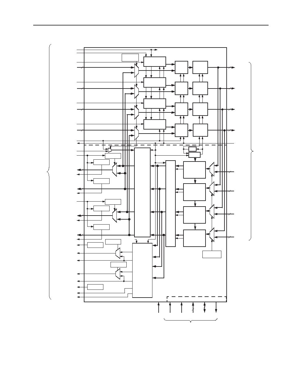
ORT4622 Overview
Device Layout
The ORT4622 FPSC provides a high-speed backplane
transceiver combined with FPGA logic. The device is
based on a 2.5 V 3.3 V I/O OR3L125B FPGA. The
OR3L125B has a 28 x 28 array of programmable logic
cells (PLCs). For the ORT4622, the bottom ten rows of
PLCs in the array were replaced with the embedded
backplane transceiver core. The ORT4622 embedded
core comprises the HSI macrocell, the synchronous
transport module (STM) macrocell, a CPU interface,
and LVDS I/Os. The four full-duplex channels perform
data transfer, scrambling/descrambling and framing at
the rate of 622 Mbits/s. Figure 1 shows the ORT4622
block diagram.
Table 2
shows a schematic view of the ORT4622. The
upper portion of the device is an 18 x 28 array of PLCs
surrounded on the left, top, and right by programmable
input/output cells (PICs). At the bottom of the PLC
array are the core interface cells (CICs) connecting to
the embedded core region. The embedded core region
contains the backplane transceiver functionality of the
device. It is surrounded on the left, bottom, and right by
backplane transceiver dedicated I/Os as well as power
and special function FPGA pins. Also shown are the
interquad routing blocks (hIQ, vIQ) present in the
Series 3 FPGA devices. System-level functions
(located in the corners of the PLC array), routing
resources, and configuration RAM are not shown in
Table 2
.
Backplane Transceiver Interface
The advantage of the ORT4622 FPSC is to bring spe-
cific networking functions to an early market presence
with programmable logic in FPGA system.
The 622 Mbits/s backplane transceiver core allows the
ORT4622 to communicate across a backplane or on a
given board at an aggregate speed of 2.5 Gbits/s, pro-
viding a physical medium for high-speed asynchronous
serial data transfer between system devices. This
device is intended for, but not limited to, connecting ter-
minal equipment in SONET/SDH and ATM systems.
For networking applications, the ORT4622 offers a
pseudo SONET framer and scrambler/descrambler
interface capable of frame synchronization and inser-
tion/extraction of selectable transport overhead bytes
and SONET scrambling and descrambling for four
STS-12 (622 Mbits/s) channels. The channels are syn-
chronized to each other by a user-provided 8 kHz
frame pulse. The ORT4622 also provides STS-48
(2.5 Gbits/s) operation across all four channels where
each channel is in STS-12 format. The pseudo-SONET
framer of OR4622 is designed with a reduced set of the
SONET framing algorithm. The pointer processing
capability is more suitable for low error rate intersystem
data communication, particular for backplane trans-
ceiver applications. Figure 2 shows the architecture of
the ORT4622 backplane transceiver core.
5-8113(F)
Figure 1.
ORCA
ORT4622 Block Diagram
∑ CLOCK/DATA
RECOVERY
4 FULL-
DUPLEX
SERIAL
CHANNELS
BYTE-
WIDE
DATA
FPGA LOGIC
STANDARD
FPGA
I/Os
LVDS
622 Mbits/s
DATA
622 Mbits/s
DATA
STM
∑ POINTER MOVER
∑ SCRAMBLING
∑ FIFO ALIGNMENT
∑ TOH PROCESSOR
I/Os
HSI
4
4

Lattice Semiconductor
8
Preliminary Data Sheet
ORCA
ORT4622 FPSC
April 2002
Four-Channel x 622 Mbits/s Backplane Transceiver
ORT4622 Overview
(continued)
Table 2
. ORT4622 Array
IIII IIII IIII IIII IIII IIII IIII IIII IIII IIII IIII IIII IIII IIII
IIII IIII IIII IIII IIII IIII IIII IIII IIII IIII IIII IIII IIII IIII
PT1
PT2
PT3
PT4
PT5
PT6
PT7
PT8
PT9
PT10
PT11
PT12
PT13
PT14
PT15
PT16
PT17
PT18
PT19
PT20
PT21
PT22
PT23
PT24
PT25
PT26
PT27
PT28
IIII
PL1
R1
C1
R1
C2
R1
C3
R1
C4
R1
C5
R1
C6
R1
C7
R1
C8
R1
C9
R1
C10
R1
C11
R1
C12
R1
C13
R1
C14
R1
C15
R1
C16
R1
C17
R1
C18
R1
C19
R1
C20
R1
C21
R1
C22
R1
C23
R1
C24
R1
C25
R1
C26
R1
C27
R1
C28
PR1
IIII
IIII
PL2
R2
C1
R2
C2
R2
C3
R2
C4
R2
C5
R2
C6
R2
C7
R2
C8
R2
C9
R2
C10
R2
C11
R2
C12
R2
C13
R2
C14
R2
C15
R2
C16
R2
C17
R2
C18
R2
C19
R2
C20
R2
C21
R2
C22
R2
C23
R2
C24
R2
C25
R2
C26
R2
C27
R2
C28
PR2
IIII
IIII
PL3
R3
C1
R3
C2
R3
C3
R3
C4
R3
C5
R3
C6
R3
C7
R3
C8
R3
C9
R3
C10
R3
C11
R3
C12
R3
C13
R3
C14
R3
C15
R3
C16
R3
C17
R3
C18
R3
C19
R3
C20
R3
C21
R3
C22
R3
C23
R3
C24
R3
C25
R3
C26
R3
C27
R3
C28
PR3
IIII
IIII
PL4
R4
C1
R4
C2
R4
C3
R4
C4
R4
C5
R4
C6
R4
C7
R4
C8
R4
C9
R4
C10
R4
C11
R4
C12
R4
C13
R4
C14
R4
C15
R4
C16
R4
C17
R4
C18
R4
C19
R4
C20
R4
C21
R4
C22
R4
C23
R4
C24
R4
C25
R4
C26
R4
C27
R4
C28
PR4
IIII
IIII
PL5
R5
C1
R5
C2
R5
C3
R5
C4
R5
C5
R5
C6
R5
C7
R5
C8
R5
C9
R5
C10
R5
C11
R5
C12
R5
C13
R5
C14
R5
C15
R5
C16
R5
C17
R5
C18
R5
C19
R5
C20
R5
C21
R5
C22
R5
C23
R5
C24
R5
C25
R5
C26
R5
C27
R5
C28
PR5
IIII
IIII
PL6
R6
C1
R6
C2
R6
C3
R6
C4
R6
C5
R6
C6
R6
C7
R6
C8
R6
C9
R6
C10
R6
C11
R6
C12
R6
C13
R6
C14
R6
C15
R6
C16
R6
C17
R6
C18
R6
C19
R6
C20
R6
C21
R6
C22
R6
C23
R6
C24
R6
C25
R6
C26
R6
C27
R6
C28
PR6
IIII
IIII
PL7
R7
C1
R7
C2
R7
C3
R7
C4
R7
C5
R7
C6
R7
C7
R7
C8
R7
C9
R7
C10
R7
C11
R7
C12
R7
C13
R7
C14
R7
C15
R7
C16
R7
C17
R7
C18
R7
C19
R7
C20
R7
C21
R7
C22
R7
C23
R7
C24
R7
C25
R7
C26
R7
C27
R7
C28
PR7
IIII
IIII
PL8
R8
C1
R8
C2
R8
C3
R8
C4
R8
C5
R8
C6
R8
C7
R8
C8
R8
C9
R8
C10
R8
C11
R8
C12
R8
C13
R8
C14
R8
C15
R8
C16
R8
C17
R8
C18
R8
C19
R8
C20
R8
C21
R8
C22
R8
C23
R8
C24
R8
C25
R8
C26
R8
C27
R8
C28
PR8
IIII
IIII
PL9
R9
C1
R9
C2
R9
C3
R9
C4
R9
C5
R9
C6
R9
C7
R9
C8
R9
C9
R9
C10
R9
C11
R9
C12
R9
C13
R9
C14
R9
C15
R9
C16
R9
C17
R9
C18
R9
C19
R9
C20
R9
C21
R9
C22
R9
C23
R9
C24
R9
C25
R9
C26
R9
C27
R9
C28
PR9
IIII
IIII
PL10
R10
C1
R10
C2
R10
C3
R10
C4
R10
C5
R10
C6
R10
C7
R10
C8
R10
C9
R10
C10
R10
C11
R10
C12
R10
C13
R10
C14
R10
C15
R10
C16
R10
C17
R10
C18
R10
C19
R10
C20
R10
C21
R10
C22
R10
C23
R10
C24
R10
C25
R10
C26
R10
C27
R10
C28
PR10
IIII
IIII
PL11
R11
C1
R11
C2
R11
C3
R11
C4
R11
C5
R11
C6
R11
C7
R11
C8
R11
C9
R11
C10
R11
C11
R11
C12
R11
C13
R11
C14
R11
C15
R11
C16
R11
C17
R11
C18
R11
C19
R11
C20
R11
C21
R11
C22
R11
C23
R11
C24
R11
C25
R11
C26
R11
C27
R11
C28
PR11
IIII
IIII
PL12
R12
C1
R12
C2
R12
C3
R12
C4
R12
C5
R12
C6
R12
C7
R12
C8
R12
C9
R12
C10
R12
C11
R12
C12
R12
C13
R12
C14
R12
C15
R12
C16
R12
C17
R12
C18
R12
C19
R12
C20
R12
C21
R12
C22
R12
C23
R12
C24
R12
C25
R12
C26
R12
C27
R12
C28
PR12
IIII
IIII
PL13
R13
C1
R13
C2
R13
C3
R13
C4
R13
C5
R13
C6
R13
C7
R13
C8
R13
C9
R13
C10
R13
C11
R13
C12
R13
C13
R13
C14
R13
C15
R13
C16
R13
C17
R13
C18
R13
C19
R13
C20
R13
C21
R13
C22
R13
C23
R13
C24
R13
C25
R13
C26
R13
C27
R13
C28
PR13
IIII
IIII
PL14
R14
C1
R14
C2
R14
C3
R14
C4
R14
C5
R14
C6
R14
C7
R14
C8
R14
C9
R14
C10
R14
C11
R14
C12
R14
C13
R14
C14
R14
C15
R14
C16
R14
C17
R14
C18
R14
C19
R14
C20
R14
C21
R14
C22
R14
C23
R14
C24
R14
C25
R14
C26
R14
C27
R14
C28
PR14
IIII
IIII
PL15
R15
C1
R15
C2
R15
C3
R15
C4
R15
C5
R15
C6
R15
C7
R15
C8
R15
C9
R15
C10
R15
C11
R15
C12
R15
C13
R15
C14
R15
C15
R15
C16
R15
C17
R15
C18
R15
C19
R15
C20
R15
C21
R15
C22
R15
C23
R15
C24
R15
C25
R15
C26
R15
C27
R15
C28
PR15
IIII
IIII
PL16
R16
C1
R16
C2
R16
C3
R16
C4
R16
C5
R16
C6
R16
C7
R16
C8
R16
C9
R16
C10
R16
C11
R16
C12
R16
C13
R16
C14
R16
C15
R16
C16
R16
C17
R16
C18
R16
C19
R16
C20
R16
C21
R16
C22
R16
C23
R16
C24
R16
C25
R16
C26
R16
C27
R16
C28
PR16
IIII
IIII
PL17
R17
C1
R17
C2
R17
C3
R17
C4
R17
C5
R17
C6
R17
C7
R17
C8
R17
C9
R17
C10
R17
C11
R17
C12
R17
C13
R17
C14
R17
C15
R17
C16
R17
C17
R17
C18
R17
C19
R17
C20
R17
C21
R17
C22
R17
C23
R17
C24
R17
C25
R17
C26
R17
C27
R17
C28
PR17
IIII
IIII
PL18
R18
C1
R18
C2
R18
C3
R18
C4
R18
C5
R18
C6
R18
C7
R18
C8
R18
C9
R18
C10
R18
C11
R18
C12
R18
C13
R18
C14
R18
C15
R18
C16
R18
C17
R18
C18
R18
C19
R18
C20
R18
C21
R18
C22
R18
C23
R18
C24
R18
C25
R18
C26
R18
C27
R18
C28
PR18
IIII
II
ASB1
ASB2
ASB3
ASB4
ASB5
ASB6
ASB7
ASB8
ASB9
ASB10
ASB11
ASB12
ASB13
ASB14
ASB15
ASB16
ASB17
ASB18
ASB19
ASB20
ASB21
ASB22
ASB23
ASB24
ASB25
ASB26
ASB27
ASB28
II
II
EMBEDDED CORE AREA
II
IIII
IIII
IIII
IIII
IIII
IIII
IIII
IIII
IIII
IIII
IIII
IIII
IIII
IIII
IIII
IIII
IIII
IIII
IIII IIII IIII IIII IIII IIII IIII IIII IIII IIII IIII IIII IIII IIII
IIII IIII IIII IIII IIII IIII IIII IIII IIII IIII IIII IIII IIII IIII

ORCA
ORT4622 FPSC
Preliminary Data Sheet
Four-Channel x 622 Mbits/s Backplane Transceiver
April 2002
9
Lattice Semiconductor
ORT4622 Overview
(continued)
HSI Interface
The high-speed interconnect (HSI) macrocell is used
for clock/data recovery and MUX/deMUX between
77.76 MHz byte-wide internal data buses and
622 Mbits/s external serial links.
The HSI interface receives four 622 Mbits/s serial input
data streams from the LVDS inputs and provides four
independent 77.76 MHz byte-wide data streams and
recovered clock to the STM macro. There is no require-
ment for bit alignment since SONET type framing will
take place inside the ORT4622 core. For transmit, the
HSI converts four byte-wide 77.76 MHz data streams
to serial streams at 622 Mbits/s at the LVDS outputs.
STM Macrocell
The STM portion of the embedded core consists of
transmitter (Tx) and receiver (Rx) sections. The
receiver receives four byte-wide data streams at
77.76 MHz and the associated clocks from the HSI. In
the Rx section, the incoming streams are SONET
framed and descrambled before they are written into a
FIFO which absorbs phase and delay variations and
allows the shift to the system clock. The TOH is then
extracted and sent out on the four serial ports. The
pointer Mover consists of three blocks: pointer inter-
preter, elastic store, and pointer generator. The pointer
interpreter finds the synchronous transport signal
(STS) synchronous payload envelopes (SPE) and
places it into a small elastic store from which the
pointer generator will produce four byte-wide STS-12
streams of data that are aligned to the system timing
pulse.
In the Tx section, transmitted data for each channel is
received through a parallel bus and a serial port from
the FPGA circuit. TOH bytes are received from the
serial input port and can be optionally inserted from
programmable registers or serial inputs to the STS-12
frame via the TOH processor. Each of the four parallel
input buses is synchronized to a free-running system
clock. Then the SPE and TOH data is transferred to the
HSI.
The STM macrocell also has a scrambler/descrambler
disable feature, allowing the user to disable the scram-
bler of the transmitter and the descrambler of the
receiver. Also, unused channels can be disabled to
reduce power dissipation.
CPU Interface
The embedded core has a dedicated, asynchronous,
MPC860 compatible, CPU interface that is used for de-
vice setup, control, and monitoring. Dual sets of I/O pins
of this CPU interface with a bit stream configurable
scheme provide designers a convenient and flexible op-
tion for configuration. One set of CPU I/O pins goes off
chip allowing direct connection with an onboard CPU.
Another set of CPU I/O pins is available to the FPGA
logic allowing for a stand-alone system free of an exter-
nal CPU interface, or for itegration into the Series 3
FPGA MPI interface.
The CPU interface is composed of an 8-bit data bus, a
7-bit address bus, a chip select signal, a read/write sig-
nal, and an interrupt signal.
FPGA Interface
The FPGA logic will receive/transmit frame-aligned
streams of 77.76 MHz data (maximum of four streams
in each direction) from/to the backplane transceiver
embedded core. All frames transmitted to the FPGA
will be aligned to the FPGA frame pulse which will be
provided by the FPGA user's logic to the STM macro.
All frames received from the FPGA logic will be aligned
to the system frame pulse that will be supplied to the
STM macro from the FPGA user's logic.
Lattice Semiconductor
10
Preliminary Data Sheet
ORCA
ORT4622 FPSC
April 2002
Four-Channel x 622 Mbits/s Backplane Transceiver
ORT4622 Overview
(continued)
5-8576 (F)
Figure 2. Architecture of ORT4622 Backplane Transceiver
TX TOH
PROCESSOR
FRAME
PROC.
TX CH A
(MACRO)
TX TOH
PROCESSOR
FRAME
PROC.
TX CH B
(MACRO)
TX TOH
PROCESSOR
FRAME
PROC.
TX CH D
(MACRO)
TX TOH
PROCESSOR
FRAME
PROC.
TX CH C
(MACRO)
LINE LBPK
(SOFT CTL)
TO RX TOH PROC.
QUAD CHANNEL
TRANSMITTER
/8
PLL
RX CH A
(MACROCELL)
77.76
MHz
FIFO
POINTER
MOVER
STS48
CH A
RX CH B
(MACROCELL)
77.76
MHz
CH B
RX CH C
(MACROCELL)
77.76
MHz
CH C
RX CH D
(MACROCELL)
77.76
MHz
CH D
LVDS LPBK
(SOFT CTL)
SOFT CTL
SOFT CTL
SOFT CTL
SOFT CTL
SOFT CTL
SOFT CTL
DEVICE I/O
RX TOH
PROCESSOR
TOH CLK
QUAD CHANNEL
RECEIVER
CH A
CH B
SOFT CTL
CH C
CH D
SOFT CTL
TOH RX B
TOH RX C
TOH RX D
RX TOH FRAME
TOH CLK
TX TOH CLK EN
TOH TX A
TOH TX B
TX BUS A
TX BUS B
TOH TX C
TX BUS C
TOH TX D
TX BUS D
SYSTEM FRAME
LINE FRAME
PROT SWITCH A/B
DATA RX BUS A
DATA RX BUS B
PROT SWITCH C/D
DATA RX BUS C
DATA RX BUS D
2
2
2
2
2
2
2
2
LVDS
OUT A
LVDS
OUT B
LVDS
OUT C
LVDS
OUT D
LVDS
IN A
LVDS
IN B
LVDS
IN C
LVDS
IN D
FPGA I/F SIGNALS
CPU INTERFACE (ASYNC)
INT_N
8
DATA
7
ADDR
RD/WR_N
CS_N
RST_N
DEVICE I/O OR FPGA I/F SIGNALS (BIT STREAM SELECTABLE)
SOFT CTL
SOFT CTL
RX TOH CLK EN
622 MHz Clks
REF
FDBK
77.76
MHz
622 MHz
77.76
MHz
FRAME
CLOCK
TOH RX A
TOH_EN
SYSTEM CLOCK
(77.76 MHz)
12
12
12
12
9
9
9
9
SYSTEM CLOCK
RX TOH CLK FPEN
DATA RX D EN
DATA RX C EN
DATA RX B EN
DATA RX A EN

Lattice Semiconductor
11
Preliminary Data Sheet
ORCA
ORT4622 FPSC
April 2002
Four-Channel x 622 Mbits/s Backplane Transceiver
ORT4622 Overview
(continued)
FPSC Configuration
Configuration of the ORT4622 occurs in two stages,
FPGA bit stream configuration and embedded core
setup.
FPGA Configuration
Prior to becoming operational, the FPGA goes through
a sequence of states, including powerup initialization,
configuration, start-up, and operation. The FPGA logic
is configured by standard FPGA bit stream configura-
tion means as discussed in the Series 3 FPGA data
sheet. Additionally, for the ORT4622, the location of the
CPU interface to the embedded core, either on the
device pins or at the FPGA/embedded core boundary,
is configured via FPGA configuration and is defined via
the ORT4622 design kit. The default configuration sets
the CPU interface pins to be active. A simple micropro-
cessor emulation soft Intellectual Property (IP) core
that uses very small FPGA logic is available from Lat-
tice. This microprocessor core sets up the embedded
core via a state machine and allows the ORT4622 to
work in an independent system without an external
microprocessor interface.
Embedded Core Setup
The embedded core operation is set up via the embed-
ded core CPU interface. All options for the operation of
the core are configured according to the device register
map presented in the detailed description section of
this data sheet.
During the powerup sequence, the ORT4622 device
(FPGA programmable circuit and the core) is held in
reset. All the LVDS output buffers and other output buff-
ers are held in 3-state. All flip-flops in core area are in
reset state, with the exception of the boundry scan shift
registers, which can only be reset by Boundary Scan
Reset. After powerup reset, the FPGA can start config-
uration. During FPGA configuration, the ORT4622 core
will be held in reset and all the local bus interface sig-
nals are forced high, but the following active-high sig-
nals (PROT_SWITCH_A, PROT_SWITCH_C,
TX_TOH_CK_EN, SYS_FP, LINE_FP) are forced low.
The CORE_READY signal sent from the embedded
core to FPGA is held low, indicating core is not ready to
interact with FPGA logic. At the end of the FPGA con-
figuration sequence, the CORE_READY signal will be
held low for six SYS_CLK cycles after DONE, TRI_IO
and RST_N (core global reset) are high. Then it will go
active-high, indicating the embedded core is ready to
function and interact with FPGA programmable circuit.
During FPGA reconfiguration when DONE and TRI_IO
are low, the CORE_READY signal sent from the core to
FPGA will be held low again to indicate the embedded
core is not ready to interact with FPGA logic. During
FPGA partial configuration, CORE_READY stays
active. The same FPGA configuration sequence
described previously will repeat again.
The initialization of the embedded core consists of two
steps: register configuration and synchronization of the
alignment FIFO. In order to configure the embedded
core, the registers need to be unlocked by writing 0xA0
to address 0x04 and writing 0x01 to address 0x05.
Control registers 0x04 and 0x05 are lock registers. If
the output bus of the data, serial TOH port, and TOH
clock and TOH frame pulse are controlled by 3-state
registers (the use of the registers for 3-state output
control is optional; these output 3-state enable signals
are brought across the local bus interface and available
to the FPGA side), the next step is to activate the 3-
state output bus and signals by taking them to func-
tional state from high-impedance state. This can be
done by writing 0x01 to correspond bits of the channel
registers 0x20, 0x38, 0x50, and 0x68. If the 3-state
control is done in FPGA logic or external logic instead
of in the embedded core registers, this step should be
done in that particular control logic also.
In addition, the synchronization of selected streams is
recommended for some networking systems applica-
tions. This is a resync of the alignment FIFO after the
enabled channels have a valid frame pulse. Here are
the procedures: Put all of the streams to be aligned,
including disabled streams, into their required align-
ment mode. Force AIS-L in all streams to be synchro-
nized (refer to register map, write 0x01 to DB1 of
register 0x20, 0x38, 0x50, 0x68). Wait four frames.
Write a 0x01 to the FIFO alignment resync register, bit
DB1 of register 0x06. Wait four frames. Release the
AIS-L in all streams (write 1 to DB1 of register 0x20,
0x38, 0x50, 0x68). This procedures allows normal data
flow through the embedded core.
Generic Backplane Transceiver
Application

12
12
Lattice Semiconductor
ORCA
ORT4622 FPSC
Preliminary Data Sheet
Four-Channel x 622 Mbits/s Backplane Transceiver
April 2002
The combination of ORT4622 and soft IP cores pro-
vides a generic data moving solution for non-SONET
applications. There is no requirement for SONET
knowledge to the users. All that is needed is to supply
the embedded core interface with data, clock, and a
8 kHz frame pulse. The provision registers may also
need to be set up, and this can be done through either
the FPGA MPI or in a state machine in the FPGA sec-
tion (VHDL code available from Lattice).
The 8 kHz frame pulse must be supplied to the
SYS_FP signal. For generic applications, the frame
pulse can be created in FPGA logic from the
77.76 MHz SYS_CLK using a simple resettable
counter (the frame pulse should only be high for one
cycle of the SYS_CLK). A VHDL core that automati-
cally provides the 8 kHz frame pulse is available from
Lattice. Byte-wide data is then sent to each of the
transmit channels as follows: the first 36 bytes trans-
ferred will be invalid data (replaced by overhead),
where the first byte is sent on the rising edge of
SYS_CLK when SYS_FP is high. The next 1044 byte
positions can be filled with valid data. This will repeat a
total of nine times (36 invalid bytes followed by 1044
valid bytes) at which time the next 8 kHz frame pulse
will be found. Thus, 87 out of 90 (96.7%) of the data
bytes sent are valid user data.
On the receive side, an 8 kHz pulse must again be sup-
plied to SYS_FP. In this case, however, only the signal
DATA_RX*_SPE must be monitored for each channel,
where a high value on this signal means valid data.
Again 87 out 90 bytes received (96.7%) will be valid
data.
In order to provide an easy user interface to transfer
arbitrary data streams through the ORT4622, Lattice
provides a soft Intellectual Property (IP) core called the
protocol independent framer, or PI-Framer. This block
transfers user format to the one described above and
allows for smoothing/rate transfer of this user data. This
framer works with a single channel at 622 Mbits/s, two
channels at 1.25 Gbits/s, or across four channels at 2.5
Gbits/s.
Backplane Transceiver Core Detailed
Description
HSI Macro
The high-speed interface (HSI) provides a physical
medium for high-speed asynchronous serial data trans-
fer between the ORT4622 and other devices. The
devices can be mounted on the same board or
mounted on different boards and connected through
the shelf backplane. The 622 Mbits/s CDR macro is a
four-channel clock phase select (CPS) and data retime
function with serial-to-parallel demultiplexing for the
incoming data stream and parallel-to-serial multiplexing
for outgoing data. The HSI macro consists of three
functionally independent blocks: receiver, transmitter,
and PLL synthesizer as shown in Figure 3.
The PLL synthesizer block receives a 77.76 MHz refer-
ence clock at its input, and provides a phase-locked
622.08 MHz clock to the transmitter block and phase
control signal to the receiver block. The PLL synthe-
sizer block is a common asset shared by four receive
and transmit channels.
The HSI receiver receives four channels of differential
622.08 Mbits/s serial data without clock at its LVDS
receive inputs. The received data must be scrambled,
conforming to SONET STS-12 and SDH STM-4 data
formats using either a PN7 or PN9 sequence. The PN7
characteristic polynomial is 1 + x
6
+ x
7
, and PN9 char-
acteristic polynomial is 1 + x
4
+ x
9
. The ORT4622 sup-
plies a default scrambler using the PN7 sequence. The
clock phase select and data retime (CPS/DR) module
performs a clock recovery and data retiming function by
using phase control information. The resultant
622.08 Mbits/s data and clock are then passed to the
deserializer module, which performs serial-to-parallel
conversion and provides a 77.76 Mbits/s parallel data
and clock at its output.
The HSI transmitter receives four channels of
77.76 Mbits/s parallel data that is synchronous to the
reference clock at its inputs. The serializer performs a
parallel-to-serial conversion using a 622.08 MHz clock
provided by the PLL/synthesizer block. The
622 Mbits/s serial data streams are then transmitted
through the LVDS drivers.

ORCA
ORT4622 FPSC
Preliminary Data Sheet
Four-Channel x 622 Mbits/s Backplane Transceiver
April 2002
13
Lattice Semiconductor
Backplane Transceiver Core Detailed Description
(continued)
5-8592 (F)
Figure 3. HSI Functional Block Diagram
622.08 MHz
PLL
SYNTHESIZER
50
50
LOOPBKEN
CLOCK/DATA
ALIGNMENT
PHASE
ADJUSTMENT
DEMUX
622 Mbits/s SERIAL TO
78 MHz PARALLEL
LOOP-
BACK
HSI_RX
622 Mbits/s
DATA
622 MHz
CLOCK
8
MUX
78 MHz PARALLEL
TO 622 Mbits/s SERIAL
BS-MUX
100
LOOP-
BACK
HDOUT
622 Mbits/s
622.08 MHz
CLOCK
HSI_TX
622 Mbits/s
DATA
(77.76 MHz REF CLOCK)
REF78
REXT
(RESISTOR)
622 Mbits/s
DATA
LVDS
BUFFER
8
(77.76 Mbytes DATA)
(77.76 Mbits/s
DATA)
(77.76 MHz
CLOCK)
77.76 MHz
77.76 Mbytes DATA
BSCANEN
HDIN
622 Mbits/s
LVDS
BUFFER
SELECT
BOUNDARY-
SCAN
CONTROL

Lattice Semiconductor
14
Preliminary Data Sheet
ORCA
ORT4622 FPSC
April 2002
Four-Channel x 622 Mbits/s Backplane Transceiver
Backplane Transceiver Core Detailed
Description
(continued)
STM Transmitter (FPGA -> Backplane)
The STM has four STS-12 transmit channels which can
be treated as a single STS-48 channel. In general, the
transmitter circuit receives four byte-wide 77.76 MHz
data from the FPGA, which nominally represents four
STS-12 streams (A, B, C, and D). This data is synchro-
nized to the system (reference) clock, and an 8 kHz
system frame pulse from the FPGA logic. Transport
overhead bytes are then optionally inserted into these
streams, and the streams are forwarded to the HSI. All
byte timing pulses required to isolate individual over-
head bytes (e.g., A1, A2, B1, D1--D3, etc.) are gener-
ated internally based on the system frame pulse
(SYS_FP) received from the FPGA logic. All streams
operate byte-wide at 77.76 MHz in all modes. The TOH
processor operates from 25 MHz to 77.76 MHz and
supports the following TOH signals: A1 and A2 inser-
tion and optional corruption; H1, H2, and H3 pass
transparently; BIP-8 parity calculation (after scram-
bling) and B1 byte insertion and optional corruption
(before scrambling); optional K1 and K2 insert; optional
S1/M0 insert; optional E1/F1/E2 insert; optional section
data communication channel (DCC, D1--D3) and line
data communication channel (DCC, D4--D12) inser-
tion (for intercard communications channel); scram-
bling of outgoing data stream with optional scrambler
disabling; and optional stream disabling.
When the ORT4622 is used in nonnetworking applica-
tions as a generic high-speed backplane data mover,
the TOH serial ports are unused or can be used for
slow-speed off-channel communication between
devices.
Data received on the parallel bus is optionally scram-
bled and transferred to LVDS outputs.
Byte Ordering Information
The core supports quad STS-12 mode of operation on
the input/output ports. STS-48 is also supported when
received in quad STS-12 format. When operating in
quad STS-12 mode, each of the independent byte
streams carries an entire STS-12 within it. Figure 4
reveals the byte ordering of the individual STS-12
streams and for STS-48 operation. Note that the recov-
ered data will always continue to be in the same order
as transmitted.
5-8574 (F)
Figure 4. Byte Ordering of Input/Output Interface in STS-12 Mode
12
24
36
48
9
21
33
45
6
18
30
42
3
15
27
39
11
23
35
47
8
20
32
44
5
17
29
41
2
14
26
38
10
22
34
46
7
19
31
43
4
16
28
40
1
13
25
37
1, 12
2, 12
3, 12
4, 12
1, 9
2, 9
3, 9
4, 9
1, 6
2, 6
3, 6
4, 6
1, 3
2, 3
3, 3
4, 3
1, 11
2, 11
3, 11
4, 11
1, 8
2, 8
3, 8
4, 8
1, 5
2, 5
3, 5
4, 5
1, 2
2, 2
3, 2
4, 2
1, 10
2, 10
3, 10
4, 10
1, 7
2, 7
3, 7
4, 7
1, 4
2, 4
3, 4
4, 4
1, 1
2, 1
3, 1
4, 1
STS-12 A
STS-12 B
STS-12 C
STS-12 D
STS-12 A
STS-12 B
STS-12 C
STS-12 D
STS-48 IN QUAD STS-12 FORMAT
QUAD STS-12

Lattice Semiconductor
15
Preliminary Data Sheet
ORCA
ORT4622 FPSC
April 2002
Four-Channel x 622 Mbits/s Backplane Transceiver
Backplane Transceiver Core Detailed
Description
(continued)
Transport Overhead for In Band Communication
The TOH byte can be used for In Band configuration,
service, and management since it is carried along the
same channel as data. In ORT4622, In Band signaling
can be efficiently utilized, since the total cost of over-
head is only 3.3%.
Transport Overhead Insertion (Serial Link)
The TOH serial links are used to insert TOH bytes into
the transmit data. The transmit TOH data and
TOH_CLK_EN get retimed by TOH_CLK in order to
meet setup and hold specifications of the device.
The retimed TOH data is shifted into a 288-bit (36-byte
by 8-bit) shift register and then multiplexed as an 8-bit
bus to be inserted into the byte-wide data stream.
Insertion from these serial links or pass-through of TOH
from the byte-wide data is under software control.
Transport Overhead Byte Ordering
(FPGA to Backplane)
In the transparent mode, SPE and TOH data received
on parallel input bus is transferred, unaltered, to the
serial LVDS output. However, B1 byte of STS#1 is
always replaced with a new calculated value (the 11
bytes following B1 are replaced with all zeros). Also, A1
and A2 bytes of all STS-1s are always regenerated.
TOH serial port in not used in the transparent mode of
operation.
In the TOH insert mode, SPE bytes are transferred,
unaltered, from the input parallel bus to the serial LVDS
output. On the other hand, TOH bytes are received
from the serial input port and are inserted in the STS-
12 frame before being sent to the LVDS output.
Although all TOH bytes from the 12 STS-1s are trans-
ferred into the device from each serial port, not all of
them get inserted in the frame. There are three hard-
coded exceptions to the TOH byte insertion:
Framing bytes (A1/A2 of all STS-1s) are not inserted
from the serial input bus. Instead, they can always be
regenerated.
Parity byte (B1 of STS#1) is not inserted from the
serial input bus. Instead, it is always recalculated (the
11 bytes following B1 are replaced with all zeros).
Pointer bytes (H1/H2/H3 of all STS-1s) are not
inserted from the serial input bus. Instead, they
always flow transparently from parallel input to LVDS
output.
In addition to the above hard-coded exceptions, the
source of some TOH bytes can be further controlled by
software. When configured to be in pass-through
mode, the specific bytes must flow transparently from
the parallel input. Note that blocks of 12 STS-1 bytes
forming an STS-12 are controlled as a whole. There
are 15 software controls per channel, as listed below:
Source of K1 and K2 bytes of the 12 STS-1s
(24 bytes) is specified by a control bit (per channel
control).
Source of S1 and M0 bytes of the 12 STS-1s
(24 bytes) is specified by a control bit (per channel
control).
Source of E1, F1, E2 bytes of the STS-1s (36 bytes)
is specified by a control it (per channel control).
Source of D1 bytes of the STS-1s (12 bytes) is spec-
ified by a control bit (per channel control).
Source of D2 bytes of the 12 STS-1s (12 bytes) is
specified by a control bit (per channel control).
Source of D3 bytes of the 12 STS-1s (12 bytes) is
specified by a control bit (per channel control).
Source of D4 bytes of the 12 STS-1s (12 bytes) is
specified by a control bit (per channel control).
Source of D5 bytes of the 12 STS-1s (12 bytes) is
specified by a control bit (per channel control).
Source of D6 bytes of the 12 STS-1s (12 bytes) is
specified by a control bit (per channel control).
Source of D7 bytes of the 12 STS-1s (12 bytes) is
specified by a control bit (per channel control).
Source of D8 bytes of the 12 STS-1s (12 bytes) is
specified by a control bit (per channel control).
Source of D9 bytes of the 12 STS-1s (12 bytes) is
specified by a control bit (per channel control).
Source of D10 bytes of the 12 STS-1s (12 bytes) is
specified by a control bit (per channel control).
Source of D11 bytes of the 12 STS-1s (12 bytes) is
specified by a control bit (per channel control).
Source of D12 bytes of the 12 STS-1s (12 bytes) is
specified by a control bit (per channel control).
TOH reconstruction is dependent on the transmitter
mode of operation. In the transparent mode of opera-
tion, TOH bytes on LVDS output are as shown in Table
3.

Lattice Semiconductor
16
Preliminary Data Sheet
ORCA
ORT4622 FPSC
April 2002
Four-Channel x 622 Mbits/s Backplane Transceiver
Backplane Transceiver Core Detailed Description
(continued)
Table 3
. Transmitter TOH on LVDS Output (Transparent Mode)
In the TOH Insert mode of operation, TOH bytes on LVDS output are shown in the following Table. This also shows
the order in which data is transferred to the serial TOH interface, starting with the must significant bit of the first A1
byte. The first bit of the first byte is replaced by an even parity check bit over all TOH bytes from the previous TOH
frame.
Table 4
. Transmitter TOH on LVDS Output (TOH Insert Mode)
A1 A1 A1 A1 A1 A1 A1 A1 A1 A1 A1 A1 A2 A2 A2 A2 A2 A2 A2 A2 A2 A2 A2 A2
B1
0
0
0
0
0
0
0
0
0
0
0
Regenerated bytes.
Transparent bytes from parallel input port.
A1 A1 A1 A1 A1 A1 A1 A1 A1 A1 A1 A1 A2 A2 A2 A2 A2 A2 A2 A2 A2 A2 A2 A2
B1
0
0
0
0
0
0
0
0
0
0
0
E1 E1 E1 E1 E1 E1 E1 E1 E1 E1 E1 E1
F1
F1
F1
F1
F1
F1
F1
F1
F1
F1
F1
F1
D1 D1 D1 D1 D1 D1 D1 D1 D1 D1 D1 D1 D2 D2 D2 D2 D2 D2 D2 D2 D2 D2 D2 D2 D3 D3 D3 D3 D3 D3 D3 D3 D3 D3 D3 D3
H1 H1 H1 H1 H1 H1 H1 H1 H1 H1 H1 H1 H2 H2 H2 H2 H2 H2 H2 H2 H2 H2 H2 H2 H3 H3 H3 H3 H3 H3 H3 H3 H3 H3 H3 H3
K1 K1 K1 K1 K1 K1 K1 K1 K1 K1 K1 K1 K2 K2 K2 K2 K2 K2 K2 K2 K2 K2 K2 K2
D4 D4 D4 D4 D4 D4 D4 D4 D4 D4 D4 D4 D5 D5 D5 D5 D5 D5 D5 D5 D5 D5 D5 D5 D6 D6 D6 D6 D6 D6 D6 D6 D6 D6 D6 D6
D7 D7 D7 D7 D7 D7 D7 D7 D7 D7 D7 D7 D8 D8 D8 D8 D8 D8 D8 D8 D8 D8 D8 D8 D9 D9 D9 D9 D9 D9 D9 D9 D9 D9 D9 D9
D10
D10
D10
D10
D10
D10
D10
D10
D10
D10
D10
D10
D11
D11
D11
D11
D11
D11
D11
D11
D11
D11
D11
D11
D12
D12
D12
D12
D12
D12
D12
D12
D12
D12
D12
D12
S1 S1 S1 S1 S1 S1 S1 S1 S1 S1 S1 S1
M0
M0
M0
M0
M0
M0
M0
M0
M0
M0
M0
M0
E2 E2 E2 E2 E2 E2 E2 E2 E2 E2 E2 E2
Regenerated bytes.
Inserted or transparent bytes. Blocks of 12 STS-1 bytes are controlled as a whole. There are 15 controls/channel: K1/K2, S1/M0, E1/F1/E2, D1, D2, D3, D4, D5, D6, D7, D8, D9, D10,
D11, D12.
Transparent bytes (from parallel input port).
Inserted bytes from TOH serial input port.

Lattice Semiconductor
17
Preliminary Data Sheet
ORCA
ORT4622 FPSC
April 2002
Four-Channel x 622 Mbits/s Backplane Transceiver
Backplane Transceiver Core Detailed
Description
(continued)
A1/A2 Frame Insert and Testing
The A1 and A2 bytes provide a special framing pattern
that indicates where a STS-1 begins in a bit stream. All
12 A1 bytes of each STS-12 are set to 0xF6, and all 12
A2 bytes of the STS-12 are set to 0x28 when not over-
ridden with an user-specified value for testing.
A1/A2 testing (corruption) is controlled per stream by
the A1/A2 error insert register. When A1/A2 corruption
detection is set for a particular stream, the A1/A2 val-
ues in the corrupted A1/A2 value registers are sent for
the number of frames defined in the corrupted A1/A2
frame count register. When the corrupted A1/A2 frame
count register is set to zero, A1/A2 corruption will con-
tinue until the A1/A2 error insert register is cleared.
On a per-device basis, the A1 and A2 byte values are
set, as well as the number of frames of corruption.
Then, to insert the specified A1/A2 values, each chan-
nel has an enable register. When the enable register is
set, the A1/A2 values are corrupted for the number
specified in the number of frames to corrupt. To insert
errors again, the per-channel fault insert register must
be cleared, and set again. Only the last A1 and the first
A2 are corrupted.
B1 Calculation and Insertion
A bit interleaved parity ≠8 (BIP-8) error check set for
even parity over all the bits of an STS-1 frame. B1 is
defined for the first STS-1 in an STS-N only. The B1
calculation block computes a BIP-8 code, using even
parity over all bits of the previous STS-12 frame after
scrambling and is inserted in the B1 byte of the current
STS-12 frame before scrambling. Per-bit B1 corruption
is controlled by the force BIP-8 corruption register (reg-
ister address 0F). For any bit set in this register, the
corresponding bit in the calculated BIP-8 is inverted
before insertion into the B1 byte position. Each stream
has an independent fault insert register that enables
the inversion of the B1 bytes. B1 bytes in all other STS-
1s in the stream are filled with zeros.
Stream Disable
When disabled via the appropriate bit in the stream
enable register, the prescrambled data for a stream is
set to all ones, feeding the HSI. The HSI macro is pow-
ered down on a per-stream basis, as are its LVDS out-
puts.
Scrambler
The data stream is scrambled using a frame synchro-
nous scrambler of sequence length 127. The scram-
bling function can be disabled by software. The
generating polynomial for the scrambler is 1 + x
6
+ x
7
.
This polynomial conforms to the standard SONET
STS-12 data format. The scrambler is reset to 1111111
on the first byte of the SPE (byte following the Z0 byte
in the twelfth STS-1). That byte and all subsequent
bytes to be scrambled are exclusive-ORed, with the
output from the byte-wise scrambler. The scrambler
runs continuously from that byte on throughout the
remainder of the frame. A1, A2, J0, and Z0 bytes are
not scrambled.
System Frame Pulse and Line Frame Pulse
System frame pulse (for transmitter) and line frame
pulse (for receiver) are generated in FPGA logic. A1/A2
framing is used on the link for locating the 8 kHz frame
location. All frames sent to the FPGA are aligned to the
FPGA frame pulse LINE_FP which is provided by the
FPGA to the STM macro. All frames sent from the
FPGA to the STM will be aligned to the frame pulse
SYS_FP that is supplied to the STM macro. In either
directions, system frame pulse and line frame pulse are
active for one system clock cycle, indicating the loca-
tion of A1 byte of STS#1. They are common to all four
channels.

18
18
Lattice Semiconductor
ORCA
ORT4622 FPSC
Preliminary Data Sheet
Four-Channel x 622 Mbits/s Backplane Transceiver
April 2002
Backplane Transceiver Core Detailed
Description
(continued)
STM Receiver (Backplane -> FPGA)
The ORT4622 has four receiving channels that can be
treated as one STS-48 stream, or treated as indepen-
dent channels. Incoming data is received through
LVDS serial ports at the data rate of 622 Mbits/s. The
receiver can handle the data streams with frame off-
sets of up to Ī12 bytes which would be due to timing
skews between cards and along backplane traces. The
received data streams are processed in the HSI and
the STM, and then passed through the CIC boundary
to the FPGA logic.
Framer Block
The framer block, in Figure 5, takes byte-wide data
from the HSI, and outputs a byte-aligned, byte-wide
data stream and 8 kHz sync pulse. The framer algo-
rithm determines the out-of-frame/in-frame status of
the incoming data and will cause interrupts on both an
errored frame and an out-of-frame (OOF) state. The
framer detects the A1/A2 framing pattern and gener-
ates the 8 kHz frame pulse. When the framer detects
OOF, it will generate an interrupt. Also, the framer
detects an errored frame and increments an A1/A2
frame error counter. The counter can be monitored by a
processor to compile performance status on the quality
of the backplane.
Because the ORT4622 is intended for use between it
and another ORT4622 or other devices via a back-
plane, there is only one errored frame state. Thus after
two transitions are missed, the state machine goes into
the OOF state and there is no severely errored frame
(SEF) or loss-of-frame (LOF) indication.
B1 Calculate and Descramble (Backplane -> FPGA)
Each Rx block receives byte-wide scrambled
77.76 MHz data and a frame sync from the framer.
Since each HSI is independently clocked, the Rx block
operates on individual streams. Timing signals required
to locate overhead bytes to be extracted are generated
internally based on the frame sync. The Rx block pro-
duces byte-wide (optionally) descrambled data and an
output frame sync for the alignment FIFO block.
The B1 calculation block computes a BIP-8 (Bit Inter-
leaved Parity 8-bits) code, using even parity over all
bits of the previous STS-12 frame before descrambling;
this value is checked against the B1 byte of the current
frame after descrambling. A per-stream B1 error
counter is incremented for each bit that is in error. The
error counter may be read via the CPU interface.
Descrambling.
The streams are descrambled using a
frame synchronous descrambler of sequence length
127 with a generating polynomial of 1 + x
6
+ x
7
. The
A1/A2 framing bytes, the section trace byte (J0) and
the growth bytes (Z0) are not descrambled. The
descrambling function can be disabled by software.
AIS-L Insertion.
Alarm indication signal (AIS) is a con-
tinuous stream of unframed 1s sent to alert down-
stream equipment that the near-end terminal has
failed, lost its signal source, or has been temporarily
taken out of service. If enabled in the AIS_L force regis-
ter, AIS-L is inserted into the received frame by writing
all ones for all bytes of the descrambled stream.
AIS-L Insertion on Out-of-Frame.
If enabled via a
register, AIS-L is inserted into the received frame by
writing all ones for all bytes of the descrambled stream
when the framer indicates that an out-of-frame condi-
tion exists.
Internal Parity Generation
Even parity is generated on all data bytes and is routed
in parallel with the data to be checked before the pro-
tection switch MUX at the parallel output.
FIFO Alignment (Backplane -> FPGA)
The alignment FIFO allows the transfer of all data to
the system clock. The FIFO sync block (Figure 5)
allows the system to be configured to allow the frame
alignment of multiple slightly varying data streams. This
optional alignment ensures that matching STS-12
streams will arrive at the FPGA end in perfect data
sync. The frame alignment is configurable to allow for
the possibility of fully independent (i.e., total frame mis-
alignment) STS-12s.

Lattice Semiconductor
19
Preliminary Data Sheet
ORCA
ORT4622 FPSC
April 2002
Four-Channel x 622 Mbits/s Backplane Transceiver
Backplane Transceiver Core Detailed
Description
(continued)
5-8577 (F)
Figure 5. Interconnect of Streams for FIFO
Alignment
The incoming data from the clock and data recovery
can be separated into four STS-12 channels (A, B, C,
and D). These streams can be frame aligned in the pat-
terns shown in Figure 6.
5-8575 (F)
Figure 6. Alignment of Four STS-12 Streams
There is also a provision to allow certain streams to be
disabled (i.e., not producing interrupts or affecting syn-
chronization). These streams can be enabled at a later
time without disrupting other streams.
The FIFO block consists of a 24 by 10-bit FIFO per link.
This FIFO is used to align up to Ī154.3 ns of interlink
skew and to transfer to the system clock. The FIFO
sync circuit takes metastable hardened frame pulses
from the write control blocks and produces sync signals
that indicate when the read control blocks should begin
reading from the first FIFO location. On top of the sync
signals, this block produces an error indicator which
indicates that the signals to be aligned are too far apart
for alignment (i.e., greater than 18 clocks apart). Sync
and error signals are sent to read control block for
alignment. The read control block is synched only once
on start-up; any further synchronization is software
controlled. The action of resynching a read control
block will always cause loss of data. A register allows
the read control block to be resynched.
Link Alignment.
The general operation of the link
alignment algorithm is to wait 12 clocks (i.e., half the
FIFO) from the arriving frame pulse and then signal the
read control block to begin reading. For perfectly
aligned frame pulses across the links, it is simply a
matter of counting down 12 and then signaling the read
control block.
The algorithm down counts by one until all of the frame
pulses have arrived and then by two when they are all
present. For example (Figure 7), if all pulses arrive
together, then alignment algorithm would count 24
(12 clocks); if, however, the arriving pulses are spread
out over four clocks, then it would count one for the first
four pulses and then two per clock afterward, which
gives a total of 14 clocks between first frame pulse and
the first read. This puts the center of arriving frame
pulses at the halfway point in the buffer. This is the
extent of the algorithm, and it has no facility for actively
correcting problems once they occur.
The write control block receives byte-wide data at
77.76 MHz and a frame pulse two clocks before the
first A1 byte of the STS-12 frame. It generates the write
address for the FIFO block. The first A1 in every STS-
12 stream is written in the same location (address 0) in
the FIFO. Also, a frame bit is passed through the FIFO
along with the first byte before the first A1 of the STS-
12. The read control block synchronizes the reading of
the FIFO for streams that are to be aligned. Reading
begins when the FIFO sync signals that all of the appli-
cable A1s and the appropriate margin have been writ-
ten to the FIFO. All of the read blocks to be
synchronized begin reading at the same time and
same location in memory (address 0).
The alignment algorithm takes the difference between
read address and write address to indicate the relative
clock alignments between STS-12 streams. If this
depth indication exceeds certain limits (12 clocks), then
an interrupt is given to the microprocessor (alignment
overflow). Each STS-12 stream can be realigned by
software if it gets too far out of line (this would cause a
loss of data). For background applications that have
less than 154.3 ns of interlink skew, misalignment will
not occur.
STS-12
STREAM A
STS-12
STREAM B
STS-12
STREAM C
STS-12
STREAM D
FIFO
SYNC
STREAM A
STREAM B
STREAM C
STREAM D
STREAM A
STREAM B
STREAM C
STREAM D

Lattice Semiconductor
20
Preliminary Data Sheet
ORCA
ORT4622 FPSC
April 2002
Four-Channel x 622 Mbits/s Backplane Transceiver
Backplane Transceiver Core Detailed Description
(continued)
5-8584 (F)
Figure 7. Examples of Link Alignment
Pointer Mover Block (Backplane -> FPGA)
The pointer mover maps incoming frames to the line framing that is supplied by the FPGA logic. The K1/K2 bytes
and H1-SS bits are also passed through to the pointer generator so that the FPGA can receive them. The pointer
mover handles both concatenations inside the STS-12, and to other STS-12s inside the core.
The pointer mover block can correctly process any length of concatenation of STS frames (multiple of three) as
long as it begins on an STS-3 boundary (i.e., STS-1 number one, four, seven, ten, etc.) and is contained within the
smaller of STS-3, 12, or 48. See details in Table 5.
Table 5
. Valid Starting Positions for an STS-Mc
STS-1
Number
STS-3cSPE
STS-6cSPE
STS-9cSPE
STS-12cSPE
STS-15cSPE
STS-18c to
STS-48c
SPEs
1
YES
YES
YES
YES
YES
YES
4
YES
YES
YES
NO
YES
--
7
YES
YES
NO
NO
YES
--
10
YES
NO
NO
NO
YES
--
13
YES
YES
YES
YES
YES
--
16
YES
YES
YES
NO
YES
--
19
YES
YES
NO
NO
YES
--
22
YES
NO
NO
NO
YES
--
25
YES
YES
YES
YES
YES
--
28
YES
YES
YES
NO
YES
--
31
YES
YES
NO
NO
YES
--
34
YES
NO
NO
NO
YES
NO
37
YES
YES
YES
YES
NO
NO
40
YES
YES
YES
NO
NO
NO
43
YES
YES
NO
NO
NO
NO
46
YES
NO
NO
NO
NO
NO
Note: YES = STS-Mc SPE can start in that STS-1.
NO = STS-Mc SPE cannot start in that STS-1.
-- = YES or NO, depending on the particular value of M.
24-byte
FIFO
24-byte
FIFO
ALL FPs
12 CLOCKS
SYNC. PULSE
ARRIVE
TOGETHER
(WRITING
BEGINS)
(READING
BEGINS)
SYNC. PULSE
(READING
BEGINS)
LAST FP
ARRIVES
4 CLOCKS
FIRST FP
ARRIVES
(WRITING
BEGINS)
10 CLOCKS
PERFECTLY ALIGNED FRAMES
4-byte SPREAD IN ARRIVING FRAMES

Lattice Semiconductor
21
Preliminary Data Sheet
ORCA
ORT4622 FPSC
April 2002
Four-Channel x 622 Mbits/s Backplane Transceiver
Backplane Transceiver Core Detailed
Description
(continued)
Pointer Interpreter State Machine.
The pointer inter-
preter's highest priority is to maintain accurate data
flow (i.e., valid SPE only) into the elastic store. This will
ensure that any errors in the pointer value will be cor-
rected by a standard, fully SONET compliant, pointer
interpreter without any data hits. This means that error
checking for increment, decrement, and new data flag
(NDF) (i.e., eight of 10) is maintained in order to ensure
accurate data flow. A single valid pointer (i.e., 0--782)
that differs from the current pointer will be ignored. Two
consecutive incoming valid pointers that differ from the
current pointer will cause a reset of the J1 location to
the latest pointer value (the generator will then produce
an NDF). This block is designed to handle single bit
errors without affecting data flow or changing state.
The pointer interpreter has only three states (NORM,
AIS, and CONC). NORM state will begin whenever two
consecutive NORM pointers are received. If two con-
secutive NORM pointers are received that both differ
from the current offset, then the current offset will be
reset to the last received NORM pointer. When the
pointer interpreter changes its offset, it causes the
pointer generator to receive a J1 value in a new posi-
tion. When the pointer generator gets an unexpected
J1, it resets its offset value to the new location and
declares an NDF. The interpreter is only looking for two
consecutive pointers that are different from the current
value. These two consecutive NORM pointers do not
have to have the same value. For example, if the cur-
rent pointer is ten and a NORM pointer with offset of 15
and a second NORM pointer with offset of 25 are
received, then the interpreter will change the current
pointer to 25. The receipt of two consecutive CONC
pointers causes CONC state to be entered. Once in
this state, offset values from the head of the concate-
nation chain are used to determine the location of the
STS SPE for each STS in the chain. Two consecutive
AIS pointers cause the AIS state to occur. Any two con-
secutive normal or concatenation pointers will end this
AIS state. This state will cause the data leaving the
pointer generator to be overwritten with 0xFF.
5-8589 (F)
Figure 8. Pointer Mover State Machine
Pointer Generator.
The pointer generator maps the
corresponding bytes into their appropriate location in
the outgoing byte stream. The generator also creates
offset pointers based on the location of the J1 byte as
indicated by the pointer interpreter. The generator will
signal NDFs when the interpreter signals that it is com-
ing out of AIS state. The pointer generator resets the
pointer value and generates NDF every time a byte
marked J1 is read from the elastic store that doesn't
match the previous offset.
Increment and decrement signals from the pointer
interpreter are latched once per frame on either the F1
or E2 byte times (depending on collisions); this ensures
constant values during the H1 through H3 times. The
choice of which byte time to do the latching on is made
once when the relative frame phases (i.e., received and
system) are determined. This latch point is then stable
unless the relative framing changes and the received H
byte times collide with the system F1 or E2 times, in
which case the latch point would be switched to the col-
lision-free byte time.
There is no restriction on how many or how often incre-
ments and decrements are processed. Any received
increment or decrement is immediately passed to the
generator for implementation regardless of when the
last pointer adjustment was made. The responsibility
for meeting the SONET criteria for maximum frequency
of pointer adjustments is left to an upstream pointer
processor.
When the interpreter signals an AIS state, the genera-
tor will immediately begin sending out 0xFF in place of
data and H1, H2, H3. This will continue until the inter-
preter returns to NORM or CONC (pointer mover state
machine) states and a J1 byte is received.
NORM
CONC
AIS
2 x CONC
2 x NORM
2 x NORM
2 x AIS
2 x CONC
2 x AIS

Lattice Semiconductor
22
Preliminary Data Sheet
ORCA
ORT4622 FPSC
April 2002
Four-Channel x 622 Mbits/s Backplane Transceiver
Backplane Transceiver Core Detailed
Description
(continued)
Transport Overhead Extraction
Transport overhead is extracted from the receive data
stream by the TOH extract block. The incoming data
gets loaded into a 36-byte shift register on the system
clock domain. This, in turn, is clocked onto the TOH
clock domain at the start of the SPE time, where it can
be clocked out.
During the SPE time, the receiver TOH frame pulse is
generated, RX_TOH_FP, which indicates the start of
the row of 36 TOH bytes. This pulse, along with the
receive TOH clock enable, RX_TOH_CK_EN, as well
as the TOH data, are all launched on the rising edge of
the TOH clock TOH_CLK.
TOH Byte Ordering (Backplane to FPGA)
The TOH processor is responsible for dropping all TOH
bytes of each channel through one of four correspond-
ing serial ports. The four TOH serial ports are synchro-
nized to the TOH clock (the same clock that is being
used by the serial ports on the transmitter side). This
free-running TOH clock is provided to the core by
external circuitry and operates at a minimum frequency
of 25 MHz and a maximum frequency of 77.76 MHz.
Data is transferred over serial links in a bursty fashion
as controlled by the Rx TOH clock enable signal, which
is generated by the ASIC and common to the four
channels. All TOH bytes of STS-12 streams are trans-
ferred over the appropriate serial link in the same order
in which they appear in a standard STS-12 frame. Data
transfer should be preformed on a row-by-row basis
such that internal data buffering needs is kept to a min-
imum. Data transfers on the serial links will be synchro-
nized relative to the Rx TOH frame signal.
Receiver TOH Reconstruction
Receiver TOH reconstruction on output parallel bus is
as shown in the following table.
Table 6
. Receiver TOH (Output Parallel Bus)
On the TOH serial port, all TOH bytes are dropped as received on the LVDS input (MSB first). The only exception is
the most significant bit of byte A1 of STS#1, which is replaced with an even parity bit. This parity bit is calculated
over the previous TOH frame. Also, on AIS-L (either resulting from LOF or forced through software), all TOH bits are
forced to all ones with proper parity (parity we automatically ends up being set to 1 on AIS-L).
Special TOH Byte Functions
K1 and K2 Handling.
The K1 and K2 bytes are used in automatic protection switch (APS) applications. K1 and K2
bytes can be optionally passed through the pointer mover under software control, or can be set to zero with the
other TOH bytes.
A1 and A2 Handling.
As discussed previously, the A1 and A2 bytes are used for a framing header. A1 and A2
bytes are always regenerated and set to hexadecimal F6 and 28, respectively.
A1 A1 A1 A1 A1 A1 A1 A1 A1 A1 A1 A1 A2 A2 A2 A2 A2 A2 A2 A2 A2 A2 A2 A2
0
0
0
0
0
0
0
0
0
0
0
0
0
0
0
0
0
0
0
0
0
0
0
0
0
0
0
0
0
0
0
0
0
0
0
0
0
0
0
0
0
0
0
0
0
0
0
0
0
0
0
0
0
0
0
0
0
0
0
0
0
0
0
0
0
0
0
0
0
0
0
0
0
0
0
0
0
0
0
0
0
0
0
0
H1 H1 H1 H1 H1 H1 H1 H1 H1 H1 H1 H1 H2 H2 H2 H2 H2 H2 H2 H2 H2 H2 H2 H2 H3 H3 H3 H3 H3 H3 H3 H3 H3 H3 H3 H3
0
0
0
0
0
0
0
0
0
0
0
0
K1
0
0
0
0
0
0
0
0
0
0
0
K2
0
0
0
0
0
0
0
0
0
0
0
0
0
0
0
0
0
0
0
0
0
0
0
0
0
0
0
0
0
0
0
0
0
0
0
0
0
0
0
0
0
0
0
0
0
0
0
0
0
0
0
0
0
0
0
0
0
0
0
0
0
0
0
0
0
0
0
0
0
0
0
0
0
0
0
0
0
0
0
0
0
0
0
0
0
0
0
0
0
0
0
0
0
0
0
0
0
0
0
0
0
0
0
0
0
0
0
0
0
0
0
0
0
0
0
0
0
0
0
0
0
0
0
0
0
0
0
0
0
0
0
0
0
0
0
0
0
0
0
0
0
0
0
0
0
0
0
0
0
0
0
0
0
0
0
Regenerated bytes.
Regenerated bytes (under pointer generator control-SS bits must be transparent-AIS-P must be supported).
Bytes taken from Elastic Store Buffer, on negative stuff opportunity-else, forced to all zeros.
Transparent or all zeros (K1/K2 are either taken from K1/K2 buffer or forced to all zeros-soft, control). In transparent mode, AIS-L must be supported.
All zero bytes.

ORCA
ORT4622 FPSC
Preliminary Data Sheet
Four-Channel x 622 Mbits/s Backplane Transceiver
April 2002
23
Lattice Semiconductor
Backplane Transceiver Core Detailed Description
(continued)
SPE and C1J1 Outputs
. These two signals for each channel are passed to the FPGA logic to allow a pointer pro-
cessor or other function to extract payload without interpreting the pointers. For the ORT4622, each frame has 12
STS-1s. In the SPE region, there are 12 J1 pulses for each STS-1s. There is one C1(J0, new SONET specifica-
tions use J0 instead of C1 as section trace to identify each STS-1 in an STS-N) pulse in the TOH area for one
frame. Thus, there is a total of 12 J1 pulses and one C1(J0) pulse per frame. C1(J0) pulse is coincident with the J0
of STS1 #1. In each frame, the SPE flag is active when the data stream is in SPE area. SPE behavior is dependent
on pointer movement and concatenation. Note that in the TOH area, H3 can also carry valid data. When valid SPE
data is carried in this H3 slot, SPE is high in this particular TOH time slot. In the SPE region, if there is no valid data
during any SPE column, the SPE signal will be set to low. SPE allow a pointer processor to extract payload without
interpreting the pointers. The SPE and C1J1 functionality are described in Table 7. For generic data operation, valid
data is available when SPE is 1 and the C1J1 signal is ignored.
Table 7
.
SPE and C1J1 Functionality
Note: The following rules are observed for generating SPE and C1J1 signals: on occurrence of AIS-P on any of the STS-1, there is no corre-
sponding J1 pulse. In case of concatenated payloads (up to STS48c), only the head STS-1 of the group has an associated J1 pulse.
C1J1 signal tracks any pointer movements. During a negative justification event, SPE is set high during the H3 byte to indicate that pay-
load data is available. During a positive justification event, SPE is set low during the positive stuff opportunity byte to indicate that payload
data is not available.
5-9330(F)
Notes: C1J1 signal behavior shown in this figure is just for illustration purposes: C1 pulse position must always be as shown; however, position
of J1 pulses vary based on path overhead location of each STS-1 within the STS-12 stream.
C1J1 signal must always be active during C1(J0) time slot of STS#1.
C1J1 signal must also be active during the twelve J1 time slots. However, C1J1 must not be active for any STS-1 for which AIS-P is gen-
erated. Also, on concatenated payloads, only the head of the group must have a J1 pulse.
Figure 9. SPE and C1J1 Functionality
SPE
C1J1
Description
0
0
TOH information excluding C1(J0) of STS1 #1.
0
1
Position of C1(J0) of STS1 #1 (one per frame). Typically used to provide a
unique link identification (256 possible unique links) to help ensure cards
are connected into the backplane correctly or cables are connected
correctly.
1
0
SPE information excluding the 12 J1 bytes.
1
1
Position of the 12 J1 bytes.
STS-12
TOH ROW # 1
SPE ROW # 1
A1 A1 A1 A1 A1 A1 A1 A1 A1 A1 A1 A1 A2 A2 A2 A2 A2 A2 A2 A2 A2 A2 A2 A2 J0 Z0 Z0 Z0 Z0 Z0 Z0 Z0 Z0 Z0 Z0 Z0
STS-12
SPE
C1J1
C1 PULSE
J1 PULSE OF
3RD STS-1
1ST SPE BYTES OF THE
12 STS-1S
1 2 3 4 5 6 7 8 9 10 11 12

Lattice Semiconductor
24
Preliminary Data Sheet
ORCA
ORT4622 FPSC
April 2002
Four-Channel x 622 Mbits/s Backplane Transceiver
Backplane Transceiver Core Detailed Description
(continued)
5-9331
Notes: SPE signal behavior shown in this figure is just for illustration purposes: SPE behavior is dependent on pointer movements and concate-
nation.
SPE signal must be high during negative stuff opportunity byte time slots (H3) for which valid data is carried (negative stuffing).
SPE signal must be low during positive stuff opportunity byte time slots for which there is no valid data (positive stuffing).
Figure 10. SPE Stuff Bytes
STS-12
TOH ROW # 4
SPE ROW # 4
H1 H1 H1 H1 H1 H1 H1 H1 H1 H1 H1 H1 H2 H2 H2 H2 H2 H2 H2 H2 H2 H2 H2 H2 H3 H3 H3 H3 H3 H3 H3 H3 H3 H3 H3 H3
STS-12
SPE
POSITIVE STUFF
OPPORTUNITY BYTES
1 2 3 4 5 6 7 8 9 10 11 12
NEGATIVE STUFF
OPPORTUNITY BYTES
SPE SIGNAL SHOWS NEGATIVE STUFFING FOR 2ND STS-1,
AND POSITIVE STUFFING FOR 6TH STS-1
Powerdown Mode
Powerdown mode will be entered when the corre-
sponding channel is disabled. Channels can be inde-
pendently enabled or disabled under software control.
Parallel data bus output enable and TOH serial data
output enable signals are made available to the FPGA
logic. The HSI macrocell's corresponding channel is
also powered down. The device will power up with all
four channels in powerdown mode.
In addition, an LVDS_EN pin has been added to control
the LVDS pins during boundary scan. During functional
operation, enabling/disabling LVDS buffers is controlled
by software registers. When in boundary scan mode,
LVDS_EN controls the enabling/disabling of LVDS buff-
ers instead of software registers. This LVDS_EN pin
should be pulled high on the board for functional opera-
tion, and pulled low during boundary scan.
Redundancy and Protection Switching
The ORT4622 supports STS-12/STS-48 redundancy
by either software or hardware control for protection
switching applications. For the transmitter mode, no
additional functionality is required for redundant opera-
tion. For receiving data, STS-12 data redundancy can
be implemented within the same device, while STS-48
and above data stream requires a pair of ORT4622
devices to support redundancy.
In STS-12 mode, the channel A receive data bus port is
used for both channel A and channel B. Similarly, the
channel C receive data bus port is used for both chan-
nel C and channel D. Channel B and channel D
become the redundant channels. The channel B and
channel D receive data bus ports are unused. Soft reg-
isters provide independent control to the protection
switching MUXes for both parallel data ports and serial
TOH data ports. When direct hardware control for pro-
tection switching is needed, external protection switch
pins are available for channels A and B, and also chan-
nels C and D. The external protection switch pins only
support parallel SPE/TOH data protection switching,
but not the serial TOH data.
In STS-48 mode, two independent devices are required
to work and protect for redundancy. Parallel and serial
port output pins on the FPGA side should be 3-stated
as the basis for supporting redundancy. The existing
local bus enable signals at the CIC can be used as 3-
state controls for FPGA data bus if needed, which can
be easily accessed by software control. Users can also
create their own protection switch 3-state enable sig-
nals either in FPGA logic or external to the device,
depending on the specific application.

ORCA
ORT4622 FPSC
Preliminary Data Sheet
Four-Channel x 622 Mbits/s Backplane Transceiver
April 2002
25
Lattice Semiconductor
Memory Map
Definition of Register Types
There are six structural register elements: sreg, creg, preg, iareg, isreg, and iereg. There are no mixed registers in
the chip. This means that all bits of a particular register (particular address) are structurally the same.
Table 8
. Structural Register Elements
Registers Access and General Description
The memory map comprises three address blocks:
Generic register block: ID, revision, scratch pad, lock, FIFO alignment, and reset registers.
Device register block: control and status bits, common to the four channels.
Channel register blocks: each of the four channels have an address block. The four address blocks have the
exact same structure with a constant address offset between channel register blocks.
All registers are write-protected by the lock register, except for the scratch pad register. The lock register is a 16-bit
read/write register. Write access is given to registers only when the key value 0xA001 is present in the lock register.
An error flag will be set upon detecting a write access when write permission is denied. The default value is
0x0000.
After powerup reset or soft reset, unused register bits will be read as zeros. Unused address locations are also
read as zeros. Write only register bits will be read as zeros. The detailed information on register access and func-
tion are described on the tables, memory map, and memory map bit description.
Element
Register
Description
sreg
Status Register A status register is read only, and, as the name implies, is used to convey the status
information of a particular element or function of the ORT4622 core. The reset value
of an sreg is really the reset value of the particular element or function that is being
read. In some cases, an sreg is really a fixed value. An example of which is the fixed
ID and revision registers.
creg
Control Register A control register is read and writable memory element inside core control. The
value of a creg will always be the value written to it. Events inside the ORT4622 core
cannot effect creg value. The only exception is a soft reset, in which case the creg
will return to its default value. The control register have default values as defined in
the default value column of Table 9.
preg
Pulse Register
Each element, or bit, of a pulse register is a control or event signal that is asserted
and then deasserted when a value of one is written to it. This means that each bit is
always of value 0 until it is written to, upon which it is pulsed to the value of one and
then returned to a value of 0. A pulse register will always have a read value of 0.
iareg
Interrupt Alarm
Register
Each bit of an interrupt alarm register is an event latch. When a particular event is
produced in the ORT4622 core, its occurrence is latched by its associated iareg bit.
To clear a particular iareg bit, a value of one must be written to it. In the ORT4622
core, all isreg reset values are 0.
isreg
Interrupt Status
Register
Each bit of an interrupt status register is physically the logical-OR function. It is a
consolidation of lower level interrupt alarms and/or isreg bits from other registers. A
direct result of the fact that each bit of the isreg is a logical-OR function means that it
will have a read value of one if any of the consolidation signals are of value one, and
will be of value 0 if and only if all consolidation signals are of value 0. In the
ORT4622 core, all isreg default values are 0.
ereg
Interrupt Enable
Register
Each bit of a status register or alarm register has an associated enable bit. If this bit
is set to value one, then the event is allowed to propagate to the next higher level of
consolidation. If this bit is set to zero, then the associated iareg or isreg bit can still
be asserted but an alarm will not propagate to the next higher level. An interrupt
enable bit is an interrupt mask bit when it is set to value 0.

Lattice Semiconductor
26
Preliminary Data Sheet
ORCA
ORT4622 FPSC
April 2002
Four-Channel x 622 Mbits/s Backplane Transceiver
Memory Map
(continued)
Memory Map Overview
Table 9
.
Memory Map
Notes:
1.Generic register block.
2.Device register block-Rx.
3.Device register block-Tx.
ADDR
[6:0]
Reg.
Type
DB7
DB6
DB5
DB4
DB3
DB2
DB1
DB0
Default
Value
(hex)
Notes
Generic Register Block
00
sreg
fixed rev [7:0]
01
1
01
sreg
fixed ID LSB [7:0]
01
02
sreg
fixed ID MSB [7:0]
A0
03
creg
scratch pad [7:0]
00
04
creg
lockreg MSB [7:0]
00
05
creg
lockreg LSB [7:0]
00
06
preg
--
--
--
--
--
--
FIFO align-
ment com-
mand
global
reset
command
NA
Device Register Block
08
creg
--
--
--
Rx TOH
frame
and
Rx TOH
clock
enable
control
ext prot
sw en
ext prot
sw
function
STS-48
STS-12 sel
(unused in
ORT4622)
LVDS
lpbk
control
00
2
09
creg
--
--
--
--
parallel
port out-
put MUX
select for
ch C
parallel
port out-
put MUX
select for
ch A
serial port
output
MUX
select for
ch C
serial port
output
MUX
select for
ch A
0F
0a
creg
--
--
--
FIFO aligner threshold value (min) [4:0]
02
0b
creg
--
--
--
FIFO aligner threshold value (max) [4:0]
15
0c
creg
--
scrambler/
descram-
bler
control
input/
output
parallel
bus parity
control
line loop-
back
control
number of consecutive A1/A2 errors to
generate [3:0]
60
3
0d
creg
A1 error insert value [7:0]
00
0e
creg
A2 error insert value [7:0]
00
0f
creg
transmitter B1 error insert mask [7:0]
00

ORCA
ORT4622 FPSC
Preliminary Data Sheet
Four-Channel x 622 Mbits/s Backplane Transceiver
April 2002
27
Lattice Semiconductor
Memory Map
(continued)
Table 9
.
Memory Map
Notes:
1.Generic register block.
2.Device register block-Rx.
3.Device register block-Tx.
4.Top-level interrupts.
5.Rx control.
6.Tx control signals.
7.Per STS#1 cos flag.
* ADDR values delimited by a comma indicate the address for each of four channels, from channel A to D. For example, the register to Tx con-
trol signals has addresses of 20, 38, 50, and 68. This indicates that channel A Tx control signals are at address 20, control B Tx control sig-
nals are at address
ADDR
[6:0]
Reg.
Type
DB7
DB6
DB5
DB4
DB3
DB2
DB1
DB0
Default
Value
(hex)
Notes
Device Register Block
(continued)
10
isreg
--
--
--
per
device int
ch D
interrupt
ch C
interrupt
ch B
interrupt
ch A
interrupt
00
4
11
iereg
--
--
--
enable/mask register [4:0]
00
12
iareg
--
--
--
--
--
--
write to
locked
register
error flag
frame
offset
error flag
00
13
iereg
--
--
--
--
--
--
enable/mask
register [1:0]
00
Channel Register Block
20, 38,
50, 68
*
creg
Protec-
tion
switching
3-state
control of
TOH data
output
Protec-
tion
switching
3-state
control of
parallel
data out-
put
channel
enable/
disable
control
parallel
output
bus parity
err ins
cmd
Rx K1/K2
source
select
TOH
serial
output
port par
err ins
cmd
force ais-l
control
Rx
behavior
in LOF
01
5
21, 39,
51, 69
creg
Tx mode
of opera-
tion
Tx E1 F1
E2 source
select
Tx S1 M0
source
select
Tx K1/K2
source
select
Tx D12
source
select
Tx D11
source
select
Tx D10
source
select
Tx D9
source
select
00
6
22, 3a,
52, 6a
creg
Tx D8
source
select
Tx D7
source
select
Tx D6
source
select
Tx D5
source
select
Tx D4
source
select
Tx D3
source
select
Tx D2
source
select
Tx D1
source
select
00
23, 3b,
53, 6b
creg
--
--
--
--
--
--
B1 error
insert
command
A1/A2
error ins
command
00
24, 3c,
54, 6c
sreg
--
--
--
--
Concatin-
dication
12
Concatin-
dication
9
Concatin-
dication
6
Concatin-
dication
3
NA 7
25, 3d,
55, 6d
sreg
Concatin-
dication
11
Concatin-
dication
8
Concatin-
dication
5
Concatin-
dication
2
Concatin-
dication
10
Concatin-
dication
7
Concatin-
dication
4
Concatin-
dication
1
NA

Lattice Semiconductor
28
Preliminary Data Sheet
ORCA
ORT4622 FPSC
April 2002
Four-Channel x 622 Mbits/s Backplane Transceiver
Memory Map
(continued)
Table 9
.
Memory Map
Notes:
1. Generic register block.
2. Device register block-Rx.
3. Device register block-Tx.
4. Top-level interrupts.
5. Rx control.
6. Tx control signals.
7. Per STS#1 cos flag.
8. Per channel interrupt.
9. Per STS-12 interrupt flags.
10. Per STS-1interrupt flags.
ADDR
[6:0]
Reg.
Type
DB7
DB6
DB5
DB4
DB3
DB2
DB1
DB0
Default
Value
(hex)
Notes
Channel Register Block
(continued)
26, 3e,
56, 6e
isreg
--
--
--
--
--
elastic
store
overflow
flag
ais-p flag
per
STS-12
alarm flag
00
8
27, 3f,
57, 6f
iereg
--
--
--
--
--
enable/mask register [2:0]
00
28, 40,
58, 70
iareg
--
--
TOH
serial
input port
parity
error flag
input
parallel
bus
parity
error flag
LVDS link
B1 parity
error flag
LOF flag Receiver
internal
path
parity
error flag
FIFO
aligner
threshold
error flag
00
9
29,41,
59, 71
iereg
--
--
enable/mask register [5:0]
00
2a, 42,
5a, 72
iareg
--
--
--
--
AIS
interrupt
flags 12
AIS
interrupt
flag 9
AIS
interrupt
flag 6
AIS
interrupt
flags 3
00
10
2b, 43,
5b, 73
iareg
AIS
interrupt
flag 11
AIS
interrupt
flag 8
AIS
interrupt
flag 5
AIS
interrupt
flag 2
AIS
interrupt
flag 10
AIS
interrupt
flag 7
AIS
interrupt
flag 4
AIS
interrupt
flag 1
00
2c, 44,
5c, 74
iereg
--
--
--
--
enable/
mask AIS
interrupt
flag 12
enable/
mask AIS
interrupt
flag 9
enable/
mask AIS
interrupt
flag 6
enable/
mask AIS
interrupt
flag 3
00
2d, 45,
5d, 75
iereg
enable/
mask AIS
interrupt
flag 11
enable/
mask AIS
interrupt
flag 8
enable/
mask AIS
interrupt
flag 5
enable/
mask AIS
interrupt
flag 2
enable/
mask AIS
interrupt
flag 10
enable/
mask AIS
interrupt
flag 7
enable/
mask AIS
interrupt
flag 4
enable/
mask AIS
interrupt
flag 1
00
2e, 46,
5e, 76
iareg
--
--
--
--
ES
overflow
flag 12
ES
overflow
flag 9
ES
overflow
flag 6
ES
overflow
flag 3
00

29
29
Lattice Semiconductor
ORCA
ORT4622 FPSC
Preliminary Data Sheet
Four-Channel x 622 Mbits/s Backplane Transceiver
April 2002
Memory Map
(continued)
Table 9
.
Memory Map
Notes:
1. Generic register block.
2. Device register block-Rx.
3. Device register block-Tx.
4. Top-level interrupts.
5. Rx control.
6. Tx control signals.
7. Per STS#1 cos flag.
8. Per channel interrupt.
9. Per STS-12 interrupt flags.
10. Per STS-1interrupt flags.
11. Binning.
ADDR
[6:0]
Reg.
Type
DB7
DB6
DB5
DB4
DB3
DB2
DB1
DB0
Default
Value
(hex)
Notes
Channel Register Block
(continued)
2f, 47,
5f, 77
iareg
ES
overflow
flag 11
ES
overflow
flag 8
ES
overflow
flag 5
ES
overflow
flag 2
ES
overflow
flag 10
ES
overflow
flag 7
ES
overflow
flag 4
ES
overflow
flag 1
00
10
30, 48,
60, 78
iereg
--
--
--
--
enable/
mask ES
overflow
flags
12
enable/
mask ES
overflow
flag
9
enable/
mask ES
overflow
flags
6
enable/
mask ES
overflow
flags
3
00
31, 49,
61, 79
iereg
enable/
mask ES
overflow
flag 11
enable/
mask ES
overflow
flag 8
enable/
mask ES
overflow
flag 5
enable/
mask ES
overflow
flag 2
enable/
mask ES
overflow
flag 10
enable/
mask ES
overflow
flag 7
enable/
mask ES
overflow
flag 4
enable/
mask ES
overflow
flag 1
00
32, 4a,
62, 7a
counter overflow
LVDS link B1 parity error counter
00
11
33, 4b,
63, 7b
counter overflow
LOF counter
00
34, 4c,
64, 7c
counter overflow
A1/A2 frame error counter
00

Lattice Semiconductor
30
Preliminary Data Sheet
ORCA
ORT4622 FPSC
April 2002
Four-Channel x 622 Mbits/s Backplane Transceiver
Memory Map
(continued)
Table 10
. Memory Map Bit Descriptions
Bit/Register
Name(s
)
Bit/
Register
Location
(hex)
Register
Type
Default
Value
(hex)
Description
Generic Register Block
fixed rev [7:0]
fixed ID LSB [7:0]
fixed ID MSB [7:0]
00 [7:0]
01 [7:0]
02 [7:0]
sreg
01
01
A0
--
scratch pad [7:0]
03 [7:0]
creg
00
The scratch pad has no function and is not used anywhere in the
ORT4622 core. However, this register can be written to and read from.
lockreg MSB [7:0]
lockreg LSB [7:0]
04 [7:0]
05 [7:0]
creg
00
00
In order to write to registers in memory locations 06 to 7F, lockreg MSB
and lockreg LSB must be respectively set to the values of A0 and 01. If
the MSB and LSB lockreg values are not set to {A0, 01}, then any values
written to the registers in memory locations 06 to 7F will be ignored.
After reset (both hard and soft), the ORT4622 core is in a write locked
mode. The ORT4622 core needs to be unlocked before it can be written
to. Also note that the scratch pad register (03) can always be written to
since it is unaffected by write lock mode.
FIFO alignment
command
global reset
command
06 [0]
06 [1]
preg
NA
The FIFO alignment and global reset commands are both accessed via
the pulse register in memory address 06. The FIFO alignment command
is used to frame align the outputs of the four receive stm stream FIFOs.
The global reset command is a soft (software initiated) reset. Neverthe-
less, the global reset command will have the exact reset effect as a hard
(RST_N pin) reset.
Device Register Block
LVDS loopback con-
trol
08 [0]
creg
0
0
No loopback.
1
LVDS loopback, transmit to receive on.
STS48 STS12 sel
08 [1]
creg
0
This control signal is untracked in the ORT4622 core. It is a scratch bit,
and its value has no effect on the ORT4622 core.
ext prot sw en
ext prot sw func
08 [3:2]
creg
0
ext
prot
sw
en
ext
prot
sw
func
Switching control master.
0
--
MUX is controlled by software (one control bit per MUX).
Output buffer 3-state signals are controlled by software (one
control bit per channel).
1
0
MUX on parallel output bus of channel A is controlled by
Prot_Switch A/B pin (0-> channel A, 1-> channel B).
MUX on parallel output bus of channel C is controlled by
Prot_Switch C/D pin (0 -> channel C, 1-> channel D).
Output buffer 3-state signals are controlled by software (one
control bit per channel).
1
1
MUX is controlled by software (one control bit per MUX).
Output buffer 3-state signals on parallel output bus of chan-
nels A and B are controlled by Prot_Switch A/B pin (0->
buffers active, 1-> hi-z).
Output buffer 3-state signals on parallel output bus of chan-
nels C and D are controlled by Prot_Switch C/D pin (0 ->
buffers active, 1-> hi-z).

ORCA
ORT4622 FPSC
Preliminary Data Sheet
Four-Channel x 622 Mbits/s Backplane Transceiver
April 2002
31
Lattice Semiconductor
Memory Map
(continued)
Table 10.
Memory Map Bit Descriptions
Bit/Register
Name(s
)
Bit/
Register
Location
(hex)
Register
Type
Default
Value
(hex)
Description
Device Register Block
(continued)
Rx TOH frame and
Rx TOH clock enable
08 [4]
creg
0
0
toh_ck_fp_en = 0, can be used to 3-state rx_toh_ck_en and
rx_toh_fp signals.
1
Functional Mode.
serial output port A
MUX select
serial output port A
MUX select
parallel output port A
MUX select
parallel output port A
MUX select
09 [0]
09 [1]
09 [2]
09 [3]
creg
1
1
1
1
TOH Output MUX Select for Port A
0
TOH output port A is multiplexed to channel B.
1
TOH output port A is multiplexed to channel A.
TOH Output MUX Select for Port C
0
TOH output port C is multiplexed to channel D.
1
TOH output port C is multiplexed to channel C.
Parallel Port Output MUX Select for Port A
0
Parallel output data bus port A is multiplexed to channel B.
1
Parallel output data bus port A is multiplexed to channel A.
Parallel Port Output MUX Select for Port C
0
Parallel output data bus port C is multiplexed to channel D.
1
Parallel output data bus port C is multiplexed to channel C.
FIFO aligner thresh-
old value (min) [4:0]
FIFO aligner thresh-
old value (max) [4:0]
0A [4:0]
0B [4:0]
creg
02
15
These are the minimum and maximum thresholds values for the per
channel receive direction alignment FIFOs. If and when the minimum or
maximum threshold value is violated by a particular channel, then the
interrupt event FIFO aligner threshold error will be generated for that
channel and latched as a FIFO aligner threshold error flag in the
respective per STS-12 interrupt alarm register.
The allowable range for minimum threshold values is 0 to 23.
The allowable range for maximum threshold values is 0 to 22.
Note that the minimal and maximum FIFO aligner threshold values
apply to all four channels.
number of consecu-
tive A1/A2 errors to
generate [3:0]
A1 error insert value
[7:0]
A2 error insert value
[7:0]
0C [3:0]
0D [7:0]
0E [7:0]
creg
00
00
00
These three-per-device control signals are used in conjunction with the
per-channel A1/A2 error insert command control bits to force A1/A2
errors in the transmit direction.
If a particular channel's A1/A2 error insert command control bit is set to
the value one, then the A1 and A2 error insert values will be inserted
into that channels respective A1 and A2 bytes. The number of consecu-
tive frames to be corrupted is determined by the number of consecutive
A1, A2 errors to generate[3:0] control bits.
The error insertion is based on a rising edge detector. As such, the con-
trol must be set to value 0 before trying to initiate a second A1/A2 cor-
ruption.
line loopback control
0C [4]
creg
0
0
No loopback.
1
Receive to transmit loopback on FPGA side.
input/output parallel
bus parity control
0C [5]
creg
0
0
Even parity.
1
Odd parity.

Lattice Semiconductor
32
Preliminary Data Sheet
ORCA
ORT4622 FPSC
April 2002
Four-Channel x 622 Mbits/s Backplane Transceiver
Memory Map
(continued)
Table 10.
Memory Map Bit Descriptions
Bit/Register Name(s
)
Bit/ Register
Location (hex)
Register
Type
Default
Value
(hex)
Description
Device Register Block
(continued)
scrambler/
descrambler control
0C [6]
creg
1
0
No receive direction descramble/transmit direction
scramble.
1
In receive direction, descramble channel after
SONET frame recovery.
In transmit direction scramble data just before paral-
lel-to-serial conversion.
transmit B1 error insert
mask [7:0]
0F [7:0]
creg
00
0
No error insertion.
1
Invert corresponding bit in B1 byte.
channel A int
channel B int
channel C int
channel D int
per device int
enable/mask register
[4:0]
10 [0]
10 [1]
10 [2]
10 [3]
10 [4]
11 [4:0]
creg
creg
creg
creg
creg
iereg
0
0
0
0
0
0
Consolidation Interrupts
0
No interrupt.
Mask interrupt in enable/mask register.
1
Interrupt.
Enable interrupt in enable/mask register.
frame offset error flag
write to locked register
error flag
enable/mask register
[1:0]
12 [0]
12 [1]
13 [1:0]
iareg
iareg
iereg
0
0
0
If in the receive direction the phase offset between any
two channels exceeds 17 bytes, then a frame offset error
event will be issued. This condition is continuously moni-
tored.
If the ORT4622 core memory map has not been unlocked
(by writing A1 00 to the lock registers), and any address
other than the lockreg registers or scratch pad register is
written to, then a write to locked register event will be gen-
erated.
Channel Register Block (Channel A, Channel B, Channel C, Channel D)
Rx behavior in LOF
20, 38 50, 68 [0]
--
1
Receive Behavior in LOF
0
When receive direction OOF occurs, do not insert
AIS-L.
1
When receive direction OOF occurs, insert AIS-L.
Force AIS-L control
20, 38, 50, 68 [1]
0
Force AIS-L Control
0
Do not force AIS-L.
1
Force AIS-L.
TOH serial output port
par err ins cmd
20, 38, 50, 68 [2]
--
0
0
Do not insert a parity error.
1
Insert parity error in parity bit of receive TOH serial
output for as long as this bit is set.
Rx K1/K2 source
select
20, 38, 50, 68 [3]
--
0
0
Set receive direction
K1/K2 bytes to 0.
1
Pass receive direction K1/K2 though pointer mover.
parallel output bus par-
ity err ins cmd
20, 38, 50, 68 [4]
--
0
0
Do not insert parity error.
1
Insert parity error in the parity bit of receive direction
parallel output bus for as long as this bit is set.
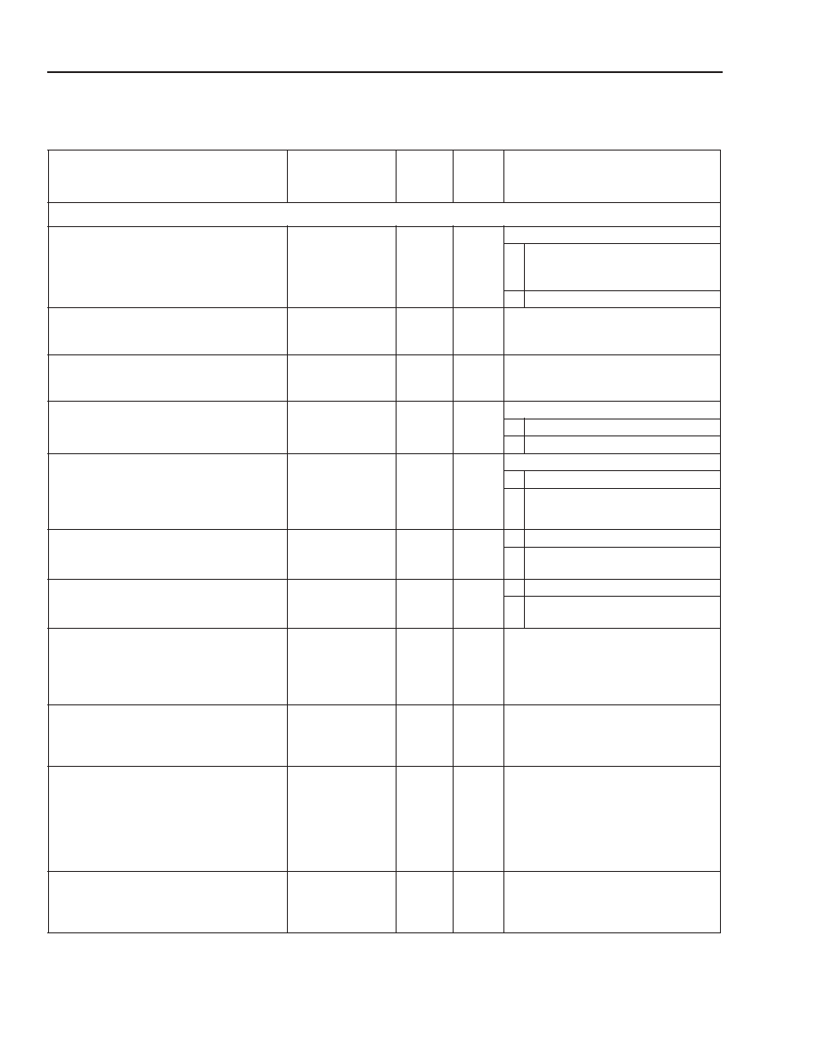
ORCA
ORT4622 FPSC
Preliminary Data Sheet
Four-Channel x 622 Mbits/s Backplane Transceiver
April 2002
33
Lattice Semiconductor
Memory Map
(continued)
Table 10.
Memory Map Bit Descriptions
* The error insertion is based on a rising edge detector. As such, the control must be set to value 0 before trying to initiate a second A1/A2
corruption.
The error insertion is based on a rising edge detector. As such, the control must be set to value 0 before trying to initiate a second B1
corruption.
Bit/Register Name(s
)
Bit/ Register
Location (hex)
Register
Type
Default
Value
(hex)
Description
Channel Register Block (Channel A, Channel B, Channel C, Channel D)
(continued)
channel enable/disable control
20, 38, 50, 68 [5]
creg
0
Channel Enable/Disable Control
0
Powerdown channel A/B/C/D CDR
and LVDS I/O can be used with
data_rx_en to 3-state output buses.
1
Functional mode.
Hi-z control of parallel output bus.
20, 38, 50, 68 [6]
creg
0
To be used as 3-state control for pro-
tection switching on the FPGA data
output.
Hi-z control of TOH data output.
20 [7]
creg
0
To be used as 3-state control for TOH
data output. Only channel A enable sig-
nal is brought out.
Tx mode of operation
21, 39, 51, 69 [7]
creg
0
Transmit Mode of Operation
0
Insert TOH from serial ports.
1
Pass through all TOH.
Tx E1 F2 E2 source select
Tx S1 M0 source select
Tx K1 K2 source select
Tx D12--D9 source select
Tx D8--D1 source select
21, 39, 51, 69 [6]
21, 39, 51, 69 [5]
21, 39, 51, 69 [4]
21, 39, 51, 69 [3:0]
22, 3a, 52, 6a [7:0]
creg
creg
creg
creg
creg
0
0
0
4'h0
8'h00
Other Registers
0
Insert TOH from serial ports.
1
Pass through that particular TOH
byte.
A1/A2 error insert command
23, 3b, 53, 6b [0]
creg
0
0
Do not insert error.*
1
Insert error for number of frames in
register hex 0C.*
B1 error insert command
23, 3b, 53, 6b [1]
creg
0
0
Do not insert error.
1
Insert error for one frame in B1 bits
defined by register hex 0F.
concatindication 12, 9, 6, 3
concatindication 11, 8, 5, 2, 10, 7, 4, 1
24, 3c, 54, 6c [3:0]
25, 3d, 55, 6d [7:0]
sreg
sreg
0
0
The value one in any bit location indi-
cates that STS# is in CONCAT mode.
A 0 indicates that the STS is not in
CONCAT mode, or is the head of a
concat group.
per STS-12 alarm flag
AIS-P flag
elastic store overflow flag
enable/mask register [2:0]
26, 3e, 56, 6e [0]
26, 3e, 56, 6e [1]
26, 3e, 56, 6e [2]
27, 3f, 57, 6f [2:0]
isreg
isreg
isreg
iereg
0
0
0
3'b000
These flag register bits per STS-12
alarm flag, AIS-P flag, and elastic store
overflow flag are the per-channel inter-
rupt status (consolidation) register.
FIFO aligner threshold error flag
receiver internal path parity error flag
LOF flag
LVDS link B1 parity error flag
input parallel bus parity error flag
TOH serial input port parity error flag
enable/mask register [5:0]
28, 40, 58, 70 [0]
28, 40, 58, 70 [1]
28, 40, 58, 70 [2]
28, 40, 58, 70 [3]
28, 40, 58, 70 [4]
28, 40, 58, 70 [5]
29, 41, 59, 71 [5:0]
iareg
iareg
iareg
iareg
iareg
iareg
iareg
0
0
0
0
0
0
6'h00
These are per the STS-12 alarm flags
with the corresponding enable/mask
register.
AIS interrupt flags 12, 9, 6, 3
AIS interrupt flags 11, 8, 5, 2, 10, 7, 4, 1
enable/mask register 12, 9, 6, 3
enable/mask register 11, 8, 5, 2, 10, 7, 4, 1
2a, 42, 5a, 72 [3:0]
2b, 43, 5b, 73 [7:0]
2c, 44, 5c, 74 [3:0]
2d, 45, 5d, 75 [7:0]
iareg
iareg
iereg
iereg
4'h0
8'h00
4'h0
8'h00
These are the AIS-P alarm flags with
the corresponding enable/mask
register.

Lattice Semiconductor
34
Preliminary Data Sheet
ORCA
ORT4622 FPSC
April 2002
Four-Channel x 622 Mbits/s Backplane Transceiver
Memory Map
(continued)
Table 10.
Memory Map Bit Descriptions
* The error insertion is based on a rising edge detector. As such, the control must be set to value 0 before trying to initiate a second A1/A2
corruption.
The error insertion is based on a rising edge detector. As such, the control must be set to value 0 before trying to initiate a second B1
corruption.
Powerup Sequencing for ORT4622 Device
ORCA
Series ORT4622 device uses two power supplies: one to power the device I/Os and the ASIC core (V
DD
),
which is set to 3.3 V for 3.3 V operation and 5 V tolerance on input pins, and another supply for the internal FPGA
logic (V
DD
2), which is set to 2.5 V. It is understood that many users will derive the 2.5 V core logic supply from a 3.3
V power supply, so the following recommendations are made for the powerup sequence of the supplies and allow-
able delays between power supplies reaching stable voltages. In general, both the 3.3 V and the 2.5 V supplies
should ramp-up and become stable as close together in time as possible. There is no delay requirement if the V
DD
2
(2.5 V) supply becomes stable prior to the V
DD
(3.3 V) supply. There is a delay requirement imposed if the V
DD
sup-
ply becomes stable prior to the V
DD
2 supply. The requirement is that the V
DD
2 (2.5 V) supply transition from
0 V to 2.3 V within 15.7 ms if the V
DD
(3.3 V) supply is already stable at a minimum of 3.0 V. If the V
DD
supply has
not yet reached 3.0 V when the V
DD
2 supply has reached 2.3 V, then the requirement is that the V
DD
2 supply reach
a minimum of 2.3 V within 15.7 ms of when the V
DD
supply reaches 3.0 V. If the chosen power supplies cannot
meet this delay requirement, it is always possible to hold off configuration of the FPGA by asserting INIT or PRGM
until the V
DD
2 supply has reached 2.3 V. This process eliminates any power supply sequencing issues.
Bit/Register Name(s
)
Bit/ Register
Location (hex)
Register
Type
Default
Value
(hex)
Description
Channel Register Block (Channel A, Channel B, Channel C, Channel D)
(continued)
ES overflow flags 12, 9, 6, 3
ES overflow flags 11, 8, 5, 2, 10, 7, 4, 1
enable/mask register 12, 9, 6, 3
enable/mask register 11, 8, 5, 2, 10, 7, 4, 1
2e, 46, 5e, 76 [7:0]
2f, 47, 5f, 77 [3:0]
30, 48, 60, 78 [7:0]
31, 49, 61, 79 [7:0]
--
4'h0
8'h00
4'h0
8'h00
These are the elastic store overflow
alarm flags.
LVDS link B1 parity error counter
32, 4a, 62, 7a [7:0]
counter
8'h00
7-bit count + overflow-reset on read.
LOF counter
33, 4b, 63, 7b [7:0]
counter
8'h00
7-bit count + overflow-reset on read.
A1/A2 frame error counter
34, 4c, 64, 7c [7:0]
counter
8'h00
7-bit count + overflow-reset on read.

Lattice Semiconductor
35
Preliminary Data Sheet
ORCA
ORT4622 FPSC
April 2002
Four-Channel x 622 Mbits/s Backplane Transceiver
FPGA Configuration Data Format
The ORCA Foundry development system interfaces
with front-end design entry tools and provides tools to
produce a fully configured FPSC. This section dis-
cusses using the ORCA Foundry development system
to generate configuration RAM data and then provides
the details of the configuration frame format.
Using ORCA Foundry to Generate Configu-
ration RAM Data
The configuration data bit stream defines the embed-
ded core configuration, the FPGA logic functionality,
and the I/O configuration and interconnection. The data
bit stream is generated by the ORCA Foundry develop-
ment tools. The bit stream created by the bit stream
generation tool is a series of 1s and 0s used to write
the FPSC configuration RAM. It can be loaded into the
FPSC using one of the configuration modes discussed
elsewhere in this data sheet.
For FPSCs, the bit stream is prepared in two separate
steps in the design flow. The configuration options of
the embedded core are specified using ORCA
ORT4622 Design Kit Software at the beginning of the
design process. This offers the designer a specific con-
figuration to simulate and design the FPGA logic to.
Upon completion of the design, the bit stream genera-
tor combines the embedded core options and the
FPGA configuration into a single bit stream for down-
load into the FPSC.
FPGA Configuration Data Frame
Configuration data can be presented to the FPSC in
two frame formats: autoincrement and explicit. A
detailed description of the frame formats is shown in
Figure 11, Figure 12, and Table 11. The two modes are
similar except that autoincrement mode uses assumed
address incrementation to reduce the bit stream size,
and explicit mode requires an address for each data
frame. In both cases, the header frame begins with a
series of 1s and a preamble of 0010, followed by a
24-bit length count field representing the total number
of configuration clocks needed to complete the loading
of the FPSC.
The mandatory ID frame contains data used to deter-
mine if the bit stream is being loaded to the correct type
of ORCA device (i.e., a bit stream generated for an
ORT4622 is being sent to an ORT4622). Error check-
ing is always enabled for Series 3+ devices, through
the use of an 8-bit checksum. One bit in the ID frame
also selects between the autoincrement and explicit
address modes for this load of the configuration data.
A configuration data frame follows the ID frame. A data
frame starts with a one-start bit pair and ends with
enough one-stop bits to reach a byte boundary. If using
autoincrement configuration mode, subsequent data
frames can follow. If using explicit mode, one or more
address frames must follow each data frame, telling the
FPSC at what addresses the preceding data frame is
to be stored (each data frame can be sent to multiple
addresses).
Following all data and address frames is the postam-
ble. The format of the postamble is the same as an
address frame with the highest possible address value
with the checksum set to all ones.

Lattice Semiconductor
36
Preliminary Data Sheet
ORCA
ORT4622 FPSC
April 2002
Four-Channel x 622 Mbits/s Backplane Transceiver
FPGA Configuration Data Format
(continued)
Figure 11. Serial Configuration Data Format--Autoincrement Mode
Figure 12. Serial Configuration Data Format--Explicit Mode
Note: For slave parallel mode, the byte containing the preamble must be 11110010. The number of leading header dummy bits must
be (n
*
8) + 4, where n is any nonnegative integer and the number of trailing dummy bits must be (n
*
8), where n is any positive
integer. The number of stop bits/frame for slave parallel mode must be (x
*
8), where x is a positive integer. Note also that the bit
stream generator tool supplies a bit stream that is compatible with all configuration modes, including slave parallel mode.
Table 11. Configuration Frame Format and Contents
Header
11110010
Preamble.
24-bit Length Count
Configuration frame length.
11111111
Trailing header--8 bits.
ID Frame
0101 1111 1111 1111
ID frame header.
Configuration Mode
00 = autoincrement, 01 = explicit.
Reserved [41:0]
Reserved bits set to 0.
ID
20-bit part ID.
Checksum
8-bit checksum.
11111111
Eight stop bits (high) to separate frames.
Configuration
Data
Frame
(repeated for each
data frame)
01
Data frame header.
Data Bits
Number of data bits depends upon device.
Alignment Bits = 0
String of 0 bits added to bit stream to make frame header, plus
data bits reach a byte boundary.
Checksum
8-bit checksum.
11111111
Eight stop bits (high) to separate frames.
Configuration
Address
Frame
00
Address frame header.
14 Address Bits
14-bit address of location to start data storage.
Checksum
8-bit checksum.
11111111
Eight stop bits (high) to separate frames.
Postamble
00
Postamble header.
11111111 111111
Dummy address.
1111111111111111
16 stop bits.
5-5759(F)
CONFIGURATION DATA
CONFIGURATION DATA
1 0
0 1
0 1
PREAMBLE LENGTH
ID FRAME
CONFIGURATION
CONFIGURATION
POSTAMBLE
CONFIGURATION HEADER
0 0
0 0
COUNT
DATA FRAME 1
DATA FRAME 2
5-5760(F)
PREAMBLE LENGTH
ID FRAME
CONFIGURATION CONFIGURATION
POSTAMBLE
CONFIGURATION HEADER
ADDRESS
ADDRESS
0 0
COUNT
DATA FRAME 1
DATA FRAME 2
FRAME 2
FRAME 1
CONFIGURATION DATA
CONFIGURATION DATA
1 0
0 1
0 1
0 0
0 0
0 0

Lattice Semiconductor
37
Preliminary Data Sheet
ORCA
ORT4622 FPSC
April 2002
Four-Channel x 622 Mbits/s Backplane Transceiver
FPGA Configuration Data Format
(continued)
Bit Stream Error Checking
There are three different types of bit stream error
checking performed in the ORCA Series 3+ FPSCs:
ID frame, frame alignment, and CRC checking.
The ID data frame is sent to a dedicated location in the
FPSC. This ID frame contains a unique code for the
device for which it was generated. This device code is
compared to the internal code of the FPSC. Any differ-
ences are flagged as an ID error. This frame is auto-
matically created by the bit stream generation program
in ORCA Foundry.
Each data and address frame in the FPSC begins with
a frame start pair of bits and ends with eight stop bits
set to 1. If any of the previous stop bits were a 0 when a
frame start pair is encountered, it is flagged as a frame
alignment error.
Error checking is also done on the FPSC for each
frame by means of a checksum byte. If an error is
found on evaluation of the checksum byte, then a
checksum/parity error is flagged.
When any of the three possible errors occur, the FPSC
is forced into an idle state, forcing INIT low. The FPSC
will remain in this state until either the
RESET
or
PRGM
pins are asserted.
If using either of the
MPI
modes to configure the FPSC,
the specific type of bit stream error is written to one of
the
MPI
registers by the FPGA configuration logic. The
PGRM
bit of the
MPI
control register can also be used
to reset out of the error condition and restart configura-
tion.
FPGA Configuration Modes
There are eight methods for configuring the FPSC. Six
of the configuration modes are selected on the M0, M1,
and M2 input and are shown in Table 12. A fourth input,
M3, is used to select the frequency of the internal oscil-
lator, which is the source for CCLK in some configura-
tion modes. The nominal frequencies of the internal
oscillator are 1.25 MHz and 10 MHz. The 1.25 MHz fre-
quency is selected when the M3 input is unconnected
or driven to a high state.
Note that the Master parallel mode of configuration that
is available in the ORCA Series 3 FPGAs is not avail-
able in the ORT4622.
More information on the general FPGA modes of con-
figuration can be found in the ORCA Series 3 data
sheet.
Table 12. Configuration Modes
* Motorola is a registered trademark of Motorola, Inc.
Intel is a registered trademark of Intel Corporation.
M2 M1 M0
CCLK
Configuration
Mode
Data
0
0
0
Output
Master Serial
Serial
0
0
1
Input
Slave Parallel
Parallel
0
1
0
Output
Microprocessor:
Motorola
* Pow-
erPC
Parallel
0
1
1
Output
Microprocessor:
Intel
i960
Parallel
1
0
0
Reserved
1
0
1
Output
Async Peripheral
Parallel
1
1
0
Reserved
1
1
1
Input
Slave Serial
Serial

Lattice Semiconductor
38
Preliminary Data Sheet
ORCA
ORT4622 FPSC
April 2002
Four-Channel x 622 Mbits/s Backplane Transceiver
Absolute Maximum Ratings
Stresses in excess of the absolute maximum ratings can cause permanent damage to the device. These are abso-
lute stress ratings only. Functional operation of the device is not implied at these or any other conditions in excess
of those given in the operations sections of this data sheet. Exposure to absolute maximum ratings for extended
periods can adversely affect device reliability.
The ORCA Series 3+ FPSCs include circuitry designed to protect the chips from damaging substrate injection cur-
rents and to prevent accumulations of static charge. Nevertheless, conventional precautions should be observed
during storage, handling, and use to avoid exposure to excessive electrical stress.
Table 13
. Absolute Maximum Ratings
Recommend Operating Conditions
Table 14
. Recommend Operating Conditions
Parameter
Symbol
Min
Max
Unit
Storage Temperature
T
stg
≠65 150 įC
I/O Supply Voltage with Respect to Ground
V
DD
--
4.2
V
Internal Supply Voltage
V
DD
2
--
3.2
Input Signal with Respect to Ground
CMOS I/O
5 V Tolerant I/O
--
--
≠0.5
≠0.5
V
DD
+ 0.3
5.8
V
V
Signal Applied to High-impedance Output
--
≠0.5
V
DD
+ 0.3
V
Maximum Package Body Temperature
--
--
220
įC
Junction Temperature
T
J
≠40
125
įC
ORT4622
Temperature Range (Ambient)
I/O Supply Voltage (V
DD
)
Internal Supply Voltage (V
DD
2)
0 įC to 70 įC
3.3 V
Ī
5%
2.5 V
Ī
5%

ORCA
ORT4622 FPSC
Preliminary Data Sheet
Four-Channel x 622 Mbits/s Backplane Transceiver
April 2002
39
Lattice Semiconductor
Electrical Characteristics
Table 15
. General Electrical Characteristics
ORT4622 Commercial: V
DD
= 3.3 V
Ī
5%, V
DD
2 = 2.5 V
Ī
5%, 0 įC < T
A
< 70 įC
.
Table 16
. Electrical Characteristics for FPGA I/O
ORT4622 Commercial: V
DD
= 3.3 V
Ī
5%, V
DD
2 = 2.5 V
Ī
5%, 0 įC < T
A
< 70 įC
.
* The pull-up resistor will externally pull the pin to a level 1.0 V below V
DD
.
Symbol
Parameter
Test Conditions
ORT4622
Unit
Min
Max
I
DDSB
Standby Current
(T
A
= 25 įC, V
DD
= 3.3 V, V
DD
2 = 2.5 V)
internal oscillator
running, no output loads, inputs at V
DD
or GND
(after configuration)
--
5.3
mA
I
DDSB
Standby Current
(T
A
= 25 įC, V
DD
= 3.3 V, V
DD
2 = 2.5 V) internal oscillator
stopped, no output loads, inputs at V
DD
or GND
(after configuration)
--
1.4
mA
V
DR
Data Retention Voltage
T
A
= 25 įC
2.3
--
V
I
PP
Powerup Current
Power supply current at approximately 1 V, within a recom-
mended power supply ramp rate of 1 ms--200 ms
2.7
--
mA
Parameter
Symbol
Test Conditions
ORT4622
Unit
Min
Max
Input Voltage:
High
Low
V
IH
V
IL
Input configured as CMOS
(clamped to V
DD
)
50% V
DD
GND ≠ 0.5
V
DD
+ 0.3
30% V
DD
V
V
Input Voltage:
High
Low
V
IH
V
IL
Input configured as 5 V tolerant
50% V
DD
GND ≠ 0.5
5.8
30% V
DD
V
V
Output Voltage:
High
Low
V
OH
V
OL
V
DD
= min, I
OH
= 6 mA or 3 mA
V
DD
= min, I
OL
= 12 mA or 6 mA
2.4
--
--
0.4
V
V
Input Leakage Current
I
L
V
DD
= max, V
IN
= V
SS
or V
DD
≠10
10
ĶA
Input Capacitance
C
IN
(T
A
= 25 įC, V
DD
= 3.3 V, V
DD
2 = 2.5 V)
test frequency = 1 MHz
--
8
pF
Output Capacitance
C
OUT
(T
A
= 25 įC, V
DD
= 3.3 V, V
DD
2 = 2.5 V)
test frequency = 1 MHz
--
9
pF
DONE Pull-up Resistor*
R
DONE
--
100
--
k
M[3:0] Pull-up Resistors*
R
M
--
100
--
k
I/O Pad Static Pull-up
Current*
I
PU
(V
DD
= 3.6 V,
V
IN
= V
SS
,
T
A
= 0 įC)
14.4
50.9
ĶA
I/O Pad Static Pull-down
Current
I
PD
(V
DD
= 3.6 V,
V
IN
= V
SS,
T
A
= 0 įC)
26
103
ĶA
I/O Pad Pull-up Resistor*
R
PU
V
DD
= all, V
IN
= V
SS
, T
A
= 0 įC
100
--
k
I/O Pad Pull-down Resistor
R
PD
V
DD
= all, V
IN
= V
DD
, T
A
= 0 įC
50
--
k

Lattice Semiconductor
40
Preliminary Data Sheet
ORCA
ORT4622 FPSC
April 2002
Four-Channel x 622 Mbits/s Backplane Transceiver
Electrical Characteristics
(continued)
Table 17
. Electrical Characteristics for Embedded Core I/O Other than LVDS I/O
Note: All outputs are driving 35 pF, except CPU data bus pins which drive 100 pF. It is assumed that the TTL buffers from the
standard-cell library can handle the 100 pF load.
Symbol
Parameter
Min
Max
Unit
V
IH
Input High Voltage (TTL input)
2.0
5.5
V
V
IL
Input Low Voltages (TTL input)
--
0.8
V
V
OH
Output High Voltage (TTL output)
2.4
--
V
V
OH
Output Low Voltage (TTL output)
--
0.4
V
HSI Circuit Specifications
Input Data
The 622 Mbits/s scrambled input data stream must
conform to SONET STS-12 and SDH STM-4 data for-
mat using either a PN7 or PN9 sequence. The PN7
characteristic is 1 + x
6
+ x
7
and the PN9 characteristic
is 1 + x
4
+ x
9
. The ORT4622 supplies a default scram-
bler using the PN7 sequence. The longest allowable
stream of nontransitional 622 Mbits/s input data is 60
bits. This sequence should not occur more often than
once per minute. An input signal phase change of no
more than 100 ps is allowed over 200 ns time interval,
which translates to a frequency change of 500 ppm.
The signal eye opening must be greater than 0.4 UIp-p
(unit interval peak-to-peak), and the unit interval for
622 Mbits/s is 1.6075 ns.
Jitter Tolerance
The input jitter tolerance of the ORT4622 is shown in
Table 18.
Table 18
. Jitter Tolerance
Generated Output Jitter
The generated output jitter is a maximum of 0.2 UIp-p
from 250 kHz to 5 MHz.
PLL
PLL requires an external 10 k
pull-down resistor.
Table 19
. PLL
Input Reference Clock
Table 20
. Input Reference Clock
Frequency
UIp-p
250 kHz
0.6
25 kHz
6.0
2 kHz
60
Parameter
Min
Max
Unit
Loop Bandwidth
--
6
MHz
Jitter Peaking
--
2
dB
Powerup Reset Duration
10
--
Ķs
Lock Acquisition
--
1
ms
Parameter
Min
Max
Frequency Deviation
--
Ī
20 ppm
Frequency Change
--
500 ppm
Phase Change in 200 ns
--
100 ps

ORCA
ORT4622 FPSC
Preliminary Data Sheet
Four-Channel x 622 Mbits/s Backplane Transceiver
April 2002
41
Lattice Semiconductor
HSI Circuit Specifications
(continued)
Power Supply Decoupling LC Circuit
The 622 MHz HSI macro contains both analog and digital circuitry. The data recovery function, for example, is
implemented as primarily a digital function, but it relies on a conventional analog phase-locked loop to provide its
622 MHz reference frequency. The internal analog phase-locked loop contains a voltage-controlled oscillator. This
circuit will be sensitive to digital noise generated from the rapid switching transients associated with internal logic
gates and parasitic inductive elements. Generated noise that contains frequency components beyond the band-
width of the internal phase-locked loop (about 3 MHz) will not be attenuated by the phase-locked loop and will
impact bit error rate directly. Thus, separate power supply pins are provided for these critical analog circuit ele-
ments.
Additional power supply filtering in the form of a LC pi filter section will be used between the power supply source
and these device pins as shown in Figure 13. The corner frequency of the LC filter is chosen based on the power
supply switching frequency, which is between 100 kHz and 300 kHz in most applications.
Capacitors C1 and C2 are large electrolytic capacitors to provide the basic cutoff frequency of the LC filter. For
example, the cutoff frequency of the combination of these elements might fall between 5 kHz and 50 kHz. Capaci-
tor C3 is a smaller ceramic capacitor designed to provide a low-impedance path for a wide range of high-frequency
signals at the analog power supply pins of the device. The physical location of capacitor C3 must be as close to the
device lead as possible. Multiple instances of capacitors C3 can be used if necessary. The recommended filter for
the HSI macro is shown below: L = 4.7
Ķ
H, RL = 1
, C1 = 0.01
Ķ
F, C2 = 0.01
Ķ
F, C3 = 4.7
Ķ
F.
5-9344(F)
Figure 13. Sample Power Supply Filter Network for Analog HSI Power Supply Pins
C2
+
C3
+
TO DEVICE
PLL_VDDA
PLL_VSSA
C1
+
FROM POWER
SUPPLY SOURCE
L

Lattice Semiconductor
42
Preliminary Data Sheet
ORCA
ORT4622 FPSC
April 2002
Four-Channel x 622 Mbits/s Backplane Transceiver
L
VDS I/O
Table 21. LVDS Driver dc Data*
* External reference, REF10 = 1.0 V Ī 3%, REF14 = 1.4 V Ī 3%
Table 22
. LVDS Driver ac Data
Parameter
Symbol
Test Conditions
Min
Typ
Max
Unit
Driver Output Voltage High, V
OA
or V
OB
V
OH
R
LOAD
= 100
Ī 1%
--
--
1.475*
V
Driver Output Voltage Low, V
OA
or V
OB
V
OL
R
LOAD
= 100
Ī 1%
0.925*
--
--
V
Driver Output Differential Voltage
V
OD
= (V
OA
≠ V
OB
)
(with External
Reference Resistor)
V
OD
R
LOAD
= 100
Ī 1%
0.25
--
0.45*
V
Driver Output Offset Voltage
V
OS
= (V
OA
+ V
OB
)/2
V
OS
R
LOAD
= 100
Ī 1%
1.125*
--
1.275*
V
Output Impedance, Single Ended
R
o
V
CM
= 1.0 V and 1.4 V
40
50
60
R
O
Mismatch Between A and B
delta R
O
V
CM
= 1.0 V and 1.4 V
--
--
10
%
Change in |V
OD
| Between 0 and 1
--
R
LOAD
= 100
Ī 1%
--
--
25
mV
Change in |V
OS
| Between 0 and 1
--
R
LOAD
= 100
Ī 1%
--
--
25
mV
Output Current
I
SA,
I
SB
Driver shorted to
ground
--
--
24
mA
Output Current
I
SAB
Drivers shorted
together
--
--
12
mA
Power-off Output Leakage
|xa|, |xb|
V
DD
= 0 V
V
PAD
, V
PADN
= 0 V--3 V
--
--
30
ĶA
Parameter
Symbol
Test Conditions
Min
Max
Unit
V
OD
Fall Time, 80% to 20%
T
FALL
Z
LOAD
= 100
Ī 1%
C
PAD
= 3 pF, C
PAD
= 3 pF
100
200
ps
V
OD
Rise Time, 20% to 80%
T
RISE
Z
LOAD
= 100
Ī 1%
C
PAD
= 3 pF, C
PAD
= 3 pF
100
200
ps
Differential Skew
|tpHLA ≠ tpLHB| or
|tpHLB ≠ tpLHA|
T
SKEW1
Any differential pair on package at 50% point
of the transition
--
50
ps
Channel-to-channel Skew
|tpDIFFm ≠ tpDIFFn|,
T
SKEW2
Any two signals on package at 0 V differential
--
--
ps
Propagation Delay Time
T
PLH
T
PHL
Z
LOAD
= 100 W Ī 1%
C
PAD
= 3 pF, C
PADN
= 3 pF
0.50
0.55
0.90
1.03
ps

ORCA
ORT4622 FPSC
Preliminary Data Sheet
Four-Channel x 622 Mbits/s Backplane Transceiver
April 2002
43
Lattice Semiconductor
LVDS I/O
(continued)
LVDS Receiver Buffer Requirements
Table 23
. LVDS Receiver dc Data
* Buffer will not produce output transition when input is open-circuited.
Note: V
DD
= 3.1 V--3.5 V, 0 įC --125 įC , slow-fast process.
Table 24
. LVDS Receiver ac Data
Table 25
. LVDS Receiver Power Consumption
Table 26. LVDS Operating Parameters
Note: Under worst-case operating condition, the LVDS driver will withstand a disabled or unpowered receiver for an
unlimited period of time without being damaged. Similarly, when outputs are short-circuited to each other or to
ground, the LVDS will not suffer permanent damage. The LVDS driver supports hot-insertion. Under a well-controlled environment,
the LVDS I/O can drive backplane as well as cable.
Parameter
Symbol
Test Conditions
Min
Typ
Max Unit
Receiver Input Voltage Range, V
IA
or
V
IB
V
I
|V
GPD
| < 925 mVdc 1 MHz
0
1.2
2.4
V
Receiver Input Differential Threshold
|V
IDTH
|
|V
GPD
| < 925 mV 400 MHz
≠100
--
100
mV
Receiver Input Differential Hysteresis
V
HYST
V
IDTHH
≠ V
IDTHL
--
--
--*
mV
Receiver Differential Input Impedance
R
IN
With built-in termination,
center-tapped
80
100
120
Symbol
Parameter
Test Conditions
Min
Max
Unit
T
PWD
Receiver Output Pulse-width Distortion
|V
IDTH
| = 100 mV
311 MHz
--
TBD
ps
T
PLH
, T
PHL
Propagation Delay Time
C
L
= 1.5 pF
0.75
0.74
1.65
1.82
ns
--
With Common-mode Variation, (0 V to 2.4 V)
C
L
= 1.5 pF
--
50
ps
T
RISE
Receiver Output Signal Rise Time, V
OD
20% to 80%
C
L
= 1.5 pF
150
350
ps
T
FALL
Receiver Output Signal Fall Time, V
OD
80% to 20%
C
L
= 1.5 pF
150
350
ps
Symbol
Parameter
Test Conditions
Min
Max
Unit
PR
dc
Receiver dc Power
dc
--
34.8
mW
PR
ac
Receiver ac Power
ac, C
L
= 1.5 pF
--
0.026
mW/MHz
Parameter
Test Conditions
Min
Normal
Max
Unit
Transmit Termination Resistor
--
--
100
--
Receiver Termination Resistor
--
--
50
--
Temperature Range
--
≠40
--
125
įC
Power Supply V
DD
--
3.1
--
3.5
V
Power Supply V
SS
--
--
0
--
V

44
44
Lattice Semiconductor
ORCA
ORT4622 FPSC
Preliminary Data Sheet
Four-Channel x 622 Mbits/s Backplane Transceiver
April 2002
Timing Characteristics
Description
The most accurate timing characteristics are reported
by the timing analyzer in the ORCA Foundry develop-
ment system. A timing report provided by the develop-
ment system after layout divides path delays into logic
and routing delays. The timing analyzer can also pro-
vide logic delays prior to layout. While this allows rout-
ing budget estimates, there is wide variance in routing
delays associated with different layouts.
The logic timing parameters noted in the Electrical
Characteristics section of this data sheet are the same
as those in the design tools. In the PFU timing, symbol
names are generally a concatenation of the PFU oper-
ating mode and the parameter type. The setup, hold,
and propagation delay parameters, defined below, are
designated in the symbol name by the SET, HLD, and
DEL characters, respectively.
The values given for the parameters are the same as
those used during production testing and speed bin-
ning of the devices. The junction temperature and sup-
ply voltage used to characterize the devices are listed
in the delay tables. Actual delays at nominal tempera-
ture and voltage for best-case processes can be much
better than the values given.
It should be noted that the junction temperature used in
the tables is generally 85 įC. The junction temperature
for the FPGA depends on the power dissipated by the
device, the package thermal characteristics (
JA
), and
the ambient temperature, as calculated in the following
equation and as discussed further in the Package
Thermal Characteristics Summary section:
T
Jmax =
T
Amax
+ (P ∑
JA
) įC
Note
: The user must determine this junction tempera-
ture to see if the delays from ORCA Foundry
should be derated based on the following derat-
ing tables.
Table 27 and Table 28 provide approximate power sup-
ply and junction temperature derating for OR3LP26B
commercial devices. The delay values in this data
sheet and reported by ORCA Foundry are shown as
1.00 in the tables. The method for determining the max-
imum junction temperature is defined in the Package
Thermal Characteristics section. Taken cumulatively,
the range of parameter values for best-case vs. worst-
case processing, supply voltage, and junction tempera-
ture can approach three to one.
Table 27. Derating for Commercial Devices (I/O
Supply V
DD
)
Table 28. Derating for Commercial Devices (I/O
Supply V
DD
2)
Note: The derating tables shown above are for a typical critical path
that contains 33% logic delay and 66% routing delay. Since the
routing delay derates at a higher rate than the logic delay,
paths with more than 66% routing delay will derate at a higher
rate than shown in the table. The approximate derating values
vs. temperature are 0.26% per įC for logic delay and 0.45%
per įC for routing delay. The approximate derating values vs.
voltage are 0.13% per mV for both logic and routing delays at
25 įC.
T
J
(įC)
Power Supply Voltage
3.0 V
3.3 V
3.6 V
≠40
0.82
0.72
0.66
0
0.91
0.80
0.72
25
0.98
0.85
0.77
85
1.00
0.99
0.90
100
1.23
1.07
0.94
125
1.34
1.15
1.01
T
J
(įC)
Power Supply Voltage
2.38 V
2.5 V
2.63 V
≠40
0.86
0.71
0.67
0
0.94
0.79
0.73
25
0.99
0.84
0.77
85
1.00
0.99
0.92
100
1.23
1.05
0.96
125
1.33
1.13
1.03

Lattice Semiconductor
45
Preliminary Data Sheet
ORCA
ORT4622 FPSC
April 2002
Four-Channel x 622 Mbits/s Backplane Transceiver
Timing Characteristics
(continued)
Propagation Delay
--The time between the specified
reference points. The delays provided are the worst-
case of the tphh and tpll delays for noninverting func-
tions, tplh and tphl for inverting functions, and tphz and
tplz for 3-state enable.
Setup Time
--The interval immediately preceding the
transition of a clock or latch enable signal, during which
the data must be stable to ensure it is recognized as
the intended value.
Hold Time
--The interval immediately following the
transition of a clock or latch enable signal, during which
the data must be held stable to ensure it is recognized
as the intended value.
3-State Enable
--The time from when a 3-state control
signal becomes active and the output pad reaches the
high-impedance state.
PFU Timing
Refer to ORCA Series 3 data sheet for the following:
Combination PFU Timing Characteristics
Sequential PFU Timing Characteristics
Ripple Mode PFU Timing Characteristics
Synchronous Memory Write Characteristics
Synchronous Memory Read Characteristics
PLC Timing
Refer to ORCA Series 3 data sheet for the following:
PFU Output MUX and Direct Routing Timing Charac-
teristics
SLIC Timing
Refer to ORCA Series 3 data sheet for the following:
Supplemental Logic and Interconnect Cell (SLIC) Tim-
ing Characteristics
PIO Timing
Refer to ORCA Series 3 data sheet for the following:
Programmable I/O (PIO) Timing Characteristics
Special Function Timing
Refer to ORCA Series 3 data sheet for the following:
Microprocessor Interface (MPI) Timing Characteristics
Programmable Clock Manager (PCM) Timing Charac-
teristics
Boundary-Scan Timing Characteristics
Clock Timing
Refer to ORCA Series 3 data sheet for the following:
ExpressCLK
(ECLK) and Fast Clock (FCLK) Timing
Characteristics
General-Purpose Clock Timing Characteristics (Inter-
nally Generated Clock)
ORT4622
ExpressCLK
to Output Delay (Pin-to-Pin)
ORT4622 Fast Clock (FCLK) to Output Delay (Pin-to-
Pin)
ORT4622 General System Clock (SCLK) to Output
Delay (Pin-to-Pin)
ORT4622 Input to ExpressCLK (ECLK) Fast Capture
Setup/Hold Time (Pin-to-Pin)
ORT4622 Input to Fast Clock Setup/Hold Time (Pin-to-
Pin)
ORT4622 Input to General System Clock Setup/Hold
Time (Pin-to-Pin)
Configuration Timing
Refer to ORCA Series 3 data sheet for Configuration
Timing Characteristics.
Readback Timing
Refer to ORCA Series 3 data sheet for Readback Tim-
ing Characteristics.

Lattice Semiconductor
46
Preliminary Data Sheet
ORCA
ORT4622 FPSC
April 2002
Four-Channel x 622 Mbits/s Backplane Transceiver
Timing Characteristics
(continued)
Table 29. ORT4622 Embedded Core and FPGA Interface Clock Operation Frequencies
ORT4622 Commercial: V
DD
= 3.3 V
Ī
5%, V
DD
2 = 2.5 V
Ī
5%, 0 įC < T
A
< 70 įC.
* The sys_clk clock frequency is based on the HSI macro specifications.
All embedded core/FPGA on-chip interface timing is available in ORCA Foundry through the STAMP timing file
included in the ORT4622 Design Kit.
Description
(T
I
= 85 įC, V
DD
= min, V
DD
2 = min)
Speed
≠7
Unit
Signal
Min
Typ
Max
sys_clk
0
--*
77.76*
MHz
toh_clk
0
25
77.76
MHz

ORCA
ORT4622 FPSC
Preliminary Data Sheet
Four-Channel x 622 Mbits/s Backplane Transceiver
April 2002
47
Lattice Semiconductor
Timing Characteristics
(continued)
Clock Timing
5-8605 (F)
Figure 14. Transmit Parallel Port Timing (Backplane
->
FPGA)
Table 30
. Timing Requirements (Transmit Parallel Port Timing)
Symbol
Parameter
Min
Nom
Max
Unit
T
P
Clock Period
12.86
--
--
ns
T
L
Clock Low Time
5.1
6.43
7.7
ns
T
H
Clock High Time
5.1
6.43
7.7
ns
T
L
T
P
T
H
FIRST A1 OF STS1 #1
FPGA_SYSCLK
SYS_FP
DATA_TX BUS
(DATA BUS
FROM FPGA
TO EMBEDDED
CORE)

Lattice Semiconductor
48
Preliminary Data Sheet
ORCA
ORT4622 FPSC
April 2002
Four-Channel x 622 Mbits/s Backplane Transceiver
Timing Characteristics
(continued)
5-8606
Figure 15. Transmit Transport Delay (FPGA
->
Backplane)
Table 31
. Timing Requirements (Transmit Transport Delay)
Symbol
Parameter
Min
Nom
Max
Unit
T
PROP
Number of Clocks of Delay from Parallel
Bus Input to LVDS Output
4
7
8
SYS_CLK
T
PROP
A1 OF STS1 #1
SYS_CLK
SYS_FP
DATA_TX BUS
(PARALLEL
DATA
FROM FPGA
TO EMBEDDED
CORE)
HDOUT
(LVDS
DATA
OUT)
FIRST A1 OF STS1 #1

ORCA
ORT4622 FPSC
Preliminary Data Sheet
Four-Channel x 622 Mbits/s Backplane Transceiver
April 2002
49
Lattice Semiconductor
Timing Characteristics
(continued)
5-8607 (F)
Figure 16. Receive Parallel Port Timing
(
Backplane
->
FPGA)
Table 32
.
Timing Requirements (Receive Parallel Port Timing)
Symbol
Parameter
Min
Nom
Max
Unit
T
P
Clock Period
12.86
--
--
ns
T
L
Clock Low Time
5.1
6.43
7.7
ns
T
H
Clock High Time
5.1
6.43
7.7
ns
T
L
T
P
T
H
SYS_CLK
LINE_FP
DATA_RX BUS
(FROM EMBEDDED
CORE TO
FPGA)
FIRST A1 OF STS1 #1
PARITY,
SPE,
C1J1 PINS

Lattice Semiconductor
50
Preliminary Data Sheet
ORCA
ORT4622 FPSC
April 2002
Four-Channel x 622 Mbits/s Backplane Transceiver
Timing Characteristics
(continued)
5-8608 (F)
* Data bus refers to 8 bits data, 1 bit parity, 1 bit SPE, and 1 bit C1J1.
Channel A or C refers to whether the PROT_SW_A or PROT_SW_C pins that are activated. For example, if the PROT_SW_A pin is
activated, the timing diagram for output bus A or C refers to output bus A.
Figure 17. Protection Switch Timing
Table 33
. Timing Requirements (Protection Switch Timing)
Symbol
Parameter
Min
Nom
Max
Unit
T
TR
Transport Delay from Latching of
PROT_SW_A/C to Actual Data Switch
7
8
9
Leading edge
SYS_CLKs
T
HIZ
Transport Delay from Latching of
PROT_SW_A/C to Actual Hi-z
4 5
6
Leading
edge
SYS_CLKs
T
CH
Propagation Delay from
SYS_CLK to HI-Z of Output Bus
--
--
25
Leading edge
SYS_CLKs
SYS_CLK
PROT_SW_A
...
OR
PROT_SW_C
...
...
...
DATA_RX BUS*
A OR C
SYS_CLK
DATA_RX BUS
A & B OR
C & D
CH A/C
CH A/C
CH A/C
CH A/C
CH B/D
T
TR
T
HIZ
T
CH
CH A & B/
CH C & D
CH A & B/
CH C & D
CH A & B/
CH C & D
CH A & B/
CH C & D

ORCA
ORT4622 FPSC
Preliminary Data Sheet
Four-Channel x 622 Mbits/s Backplane Transceiver
April 2002
51
Lattice Semiconductor
Timing Characteristics
(continued)
5-8609 (F)
Figure 18. TOH Input Serial Port Timing (FPGA
->
Backplane)
Table 34
. Timing Requirements (TOH Input Serial Port Timing)
Symbol
Parameter
Min
Nom
Max
Unit
T
P
Clock Period
12.86
--
40
ns
T
HI
Clock High Time
5.1
6.43
7.7
ns
T
LO
Clock Low Time
5.1
6.43
7.7
ns
SYS_CLK
SYS_FP
...
...
...
...
DATA_TX BUS
TOH_CLK
1044 bytes SPE
...
...
TX TOH_
(PARALLEL
BUS)
TOH SERIAL
INPUT
CLK_ENA
ROW #1
ROW #9
36 bytes TOH
1044 bytes SPE
36 bytes TOH
GUARD BAND
(4 TOH CLK)
GUARD BAND
(4 TOH CLK)
MSbit(7)
OF B1 byte
STS1 #1
bit 6
OF B1 byte
STS1 #1
T
P
T
HI
T
LO

Lattice Semiconductor
52
Preliminary Data Sheet
ORCA
ORT4622 FPSC
April 2002
Four-Channel x 622 Mbits/s Backplane Transceiver
Timing Characteristics
(continued)
5-8610 (F)
Note: The total delay from A1 STS1 #1 arriving at LVDS input to RX_TOH_FP is 56 SYS_CLKs and 6 TOH_CLKs. This will vary by Ī14
SYS_CLKs, 12 each way for the FIFO alignment, and Ī2 SYS_CLKs due to the variability in the clock recovery of the HSI macro.
Figure 19. TOH Output Serial Port Timing (Backplane
->
FPGA)
Table 35
. Timing Requirements (TOH Output Serial Port Timing)
Symbol
Parameter
Min
Nom
Max
Unit
T
TRANS_SYS
Delay from First A1 LVDS Serial Input to
Transfer to TOH_CLK
44
56
68
SYS_CLKs
T
TRANS_TOH
Delay from Transfer to TOH_CLK to
RX_TOH_FP
--
6
--
TOH_CLKs
RX TOH FP
HDIN
TOH_CLK
1044 bytes SPE
RX TOH
(INPUT LVDS
SERIAL 622M
DATA)
TOH SERIAL
OUTPUT
CLK ENA
ROW #1
ROW #9
36 bytes TOH
1044 bytes SPE
36 bytes TOH
MSbit(7)
OF A1 byte
STS #1
bit 6
OF A1 byte
STS #1
T
TRANS_SYS
T
TRANS_TOH
bit 0
OF A1 byte
STS #1
...
...
...
...
...

ORCA
ORT4622 FPSC
Preliminary Data Sheet
Four-Channel x 622 Mbits/s Backplane Transceiver
April 2002
53
Lattice Semiconductor
Timing Characteristics
(continued)
5-8611 (F)
Note: The CPU interface can be bit stream selected either from device I/O or FPGA interface. The timing diagram applies to both interfaces, but
not to the FPGA MPI block.
Figure 20. CPU Write Transaction
Table 36
. Timing Requirements (CPU Write Transaction)
Symbol
Parameter
Min
Max
Unit
T
PULSE
Minimum Pulse Width for CS_N
5
--
ns
T
ADDR_MAX
Maximum Time from Negative Edge
of CS_N to ADDR Valid
--
18
ns
T
DAT_MAX
Maximum Time from Negative Edge
of CS_N to Data Valid
--
25
ns
T
RD_WR_MAX
Maximum Time from Negative Edge
of CS_N to Negative Edge of RD_WR_N
--
26
ns
T
WRITE_MAX
Maximum Time from Negative Edge of CS_N to
Contents of Internal Register Latching DB[7:0]
--
60 ns
T
ACCESS_MIN
Minimum Time Between a Write Cycle (falling
edge of CS_N) and Any Other Transaction
(read or write at falling edge of CS_N)
60
--
ns
T
INT_MAX
Maximum Time from Register FF to Pad
--
20
ns
T
RW_WR_N,
ADDR, DB_HOLD
Minimum Hold Time that RD_WR_N,
ADDR and DB Must be Held Valid from
the Negative Edge of CS_N
57
--
ns
DATA VALID
T
ACCESS_MIN
T
PULSE
OLD VALUE
NEW VALUE
T
WRITE_MAX
T
INT_MAX
T
ADDR_MAX
T
DAT_MAX RD_WR_MAX
CPU_CS_N
CPU_RD_WR_N
CPU_ADDR[6:0]
CPU_DATA[7:0]
INTERNAL REGISTER
(SYS_CLK
DOMAIN)
CPU_INT_N
T
RD_WR_N, ADDR_MAX, DB_HOLD
(CS_N)
(RD_WR_N)
(ADDR[6:0])
(DB[7:0])
(INT_N)

Lattice Semiconductor
54
Preliminary Data Sheet
ORCA
ORT4622 FPSC
April 2002
Four-Channel x 622 Mbits/s Backplane Transceiver
Timing Characteristics
(continued)
5-8612 (F)
Notes:
The CPU interface can be bit stream selected either from device I/O or FPGA interface. The timing diagram applies to both interfaces, but not to
the FPGA MPI block.
The time delay between the advanced SYS_CLK and the distributed SYS_CLK used to sample CS_N is of no consequence. However, the
path delay of CS_N from pad to where is it sampled by SYS_CLK must be minimized.
The calculated delays assume a 100 pF loading on the DB pins.
Figure 21. CPU Read Transaction
Table 37
. Timing Requirements (CPU Read Transaction)
Symbol
Parameter
Min
Max
Unit
T
PULSE
Minimum Pulse Width for CS_N
5
--
ns
T
ADDR_MAX
Maximum Time from Negative Edge of
CS_N to ADDR Valid
--
5
ns
T
RD_WR_MAX
Maximum Time from Negative Edge of
CS_N to RD_WR_N Falling
--
5
ns
T
DATA_MAX
Maximum Time from Negative Edge of
CS_N to Data Valid on DB Port
--
56
ns
T
HIZ_MAX
Maximum Time from Rising Edge of
CS_N to DB Port Going HI-Z
--
12
ns
T
ACCESS_MIN
Minimum Time Between a Read Cycle
(falling edge of CS_N) and Any Other Transaction
(read or write at falling edge of CS_N)
60
--
ns
DATA VALID
T
ACCESS_MIN
T
PULSE
T
DATA_MAX
CPU_CS_N
CPU_RD_WR_N
CPU_ADDR[6:0]
CPU_DATA[7:0]
T
HIZ_MAX
T
ADDR_MAX
T
RD_WR_MAX
(CS_N)
(RD_WR_N)
(ADDR[6:0])
(DB[7:0])
ORCA
ORT4622 FPSC
Preliminary Data Sheet
Four-Channel x 622 Mbits/s Backplane Transceiver
April 2002
55
Lattice Semiconductor
Input/Output Buffer Measurement Conditions (on-LVDS Buffer)
Note: Switch to V
DD
for
T
PLZ
/T
PZL
; switch to GND for T
PHZ
/T
PZH
.
Figure 22. ac Test Loads
5-3233.a(F)
Figure 23. Output Buffer Delays
5-3235(F)
Figure 24. Input Buffer Delays
5-3234(F)
50 pF
A. Load Used to Measure Propagation Delay
TO THE OUTPUT UNDER TEST
TO THE OUTPUT UNDER TEST
50 pF
V
CC
GND
1 k
B. Load Used to Measure Rising/Falling Edges
V
DD
T
PHH
V
DD
/2
V
SS
out[i]
PAD
OUT
1.5 V
0.0 V
T
PLL
PAD
out[i]
ac TEST LOADS (SHOWN ABOVE)
ts[i]
OUT
0.0 V
1.5 V
T
PHH
T
PLL
PAD
in[i]
IN
3.0 V
V
SS
V
DD
/2
V
DD
PAD IN
in[i]

56
56
Lattice Semiconductor
ORCA
ORT4622 FPSC
Preliminary Data Sheet
Four-Channel x 622 Mbits/s Backplane Transceiver
April 2002
FPGA Output Buffer Characteristics
5-6865(F)
Figure 25. Sinklim (T
J
= 25 įC, V
DD
= 3.3 V)
5-6867(F)
Figure 26. Slewlim (T
J
= 25 įC, V
DD
= 3.3 V)
5-6867(F)
Figure 27. Fast (T
J
= 25 įC, V
DD
= 3.3 V)
5-6866(F)
Figure 28. Sinklim (T
J
= 125 įC, V
DD
= 3.0 V)
5-6868(F)
Figure 29. Slewlim (T
J
= 125 įC, V
DD
= 3.0 V)
5-6868(F)
Figure 30. Fast (T
J
= 125 įC, V
DD
= 3.0 V)
0.0
0.5
1.0
1.5
2.0
2.5
3.0
3.5
0
20
40
60
110
OUTPUT VOLTA
GE, V
O
(V)
I
OL
70
50
30
10
I
OH
OUTPUT CURRENT, I
O
(mA)
80
90
100
0.0
0.5
1.0
1.5
2.0
2.5
3.0
0
40
80
OUTPUT VOLTAGE, V
O
(V)
I
OL
100
60
20
I
OH
OUTPUT CURRENT, I
O
(mA)
120
140
3.5
0.0
0.5
1.0
1.5
2.0
2.5
3.0
0
40
80
OUTPUT VOLTAGE, V
O
(V)
I
OL
100
60
20
I
OH
OUTPUT CURRENT, I
O
(mA)
120
140
3.5
0.0
0.5
1.0
1.5
2.0
2.5
3.0
0
20
40
60
OUTPUT VOLTAGE, V
O
(V)
I
OL
70
50
30
10
I
OH
OUTPUT CURRENT, I
O
(mA)
80
90
0.0
0.5
1.0
1.5
2.0
2.5
3.0
0
40
80
OUTPUT VOLTAGE, V
O
(V)
I
OL
100
60
20
I
OH
OUTPUT CURRENT, I
O
(mA)
120
0.0
0.5
1.0
1.5
2.0
2.5
3.0
0
40
80
OUTPUT VOLTAGE, V
O
(V)
I
OL
100
60
20
I
OH
OUTPUT CURRENT, I
O
(mA)
120

ORCA
ORT4622 FPSC
Preliminary Data Sheet
Four-Channel x 622 Mbits/s Backplane Transceiver
April 2002
57
Lattice Semiconductor
LVDS Buffer Characteristics
Termination Resistor
The LVDS drivers and receivers operate on a 100
differential impedance, as shown below. External resistors are
not required. The differential driver and receiver buffers include termination resistors inside the device package as
shown in Figure 31 below.
5-8703(F)
Figure 31. LVDS Driver and Receiver and Associated Internal Components
LVDS Driver Buffer Capabilities
Under worst-case operating condition, the LVDS driver must withstand a disabled or unpowered receiver for an
unlimited period of time without being damaged. Similarly, when its outputs are short-circuited to each other or to
ground, the LVDS driver will not suffer permanent damage. Figure 32 illustrates the terms associated with LVDS
driver and receiver pairs.
5-8704(F)
Figure 32. LVDS Driver and Receiver
5-8705(F)
Figure 33. LVDS Driver
LVDS DRIVER
50
50
LVDS RECEIVER
CENTER TAP
DEVICE PINS
100
EXTERNAL
V
GPD
V
OA
V
OB
V
IA
V
IB
A
B
AA
BB
DRIVER INTERCONNECT
RECEIVER
V
OA
A
V
OB
B
C
A
C
B
R
LOAD
V
OD
= (V
OA
≠ V
OB
)
V

Lattice Semiconductor
58
Preliminary Data Sheet
ORCA
ORT4622 FPSC
April 2002
Four-Channel x 622 Mbits/s Backplane Transceiver
Estimating Power Dissipation
The total operating power dissipated is estimated by summing the FPGA standby (I
DDSB
), internal, and external
power dissipated, in addition to the embedded block power.
Table 38
. Embedded Block Power Dissipation
Note: Power is calculated assuming an activity factor of 20%.
The following discussion relates to the FPGA portion of the device. The internal and external power is the power
consumed in the PLCs and PICs, respectively. In general, the standby power is small and may be neglected. The
total operating power is as follows:
P
T
=
P
PLC
+
P
PIC
The internal operating power is made up of two parts: clock generation and PFU output power. The PFU output
power can be estimated based upon the number of PFU outputs switching when driving an average fan-out of two:
P
PFU
= 0.078 mW/MHz
For each PFU output that switches, 0.136 mW/MHz needs to be multiplied times the frequency (in MHz) that the
output switches. Generally, this can be estimated by using one-half the clock rate, multiplied by some activity fac-
tor; for example, 20%.
The power dissipated by the clock generation circuitry is based upon four parts: the fixed clock power, the power/
clock branch row or column, the clock power dissipated in each PFU that uses this particular clock, and the power
from the subset of those PFUs that are configured as synchronous memory. Therefore, the clock power can be cal-
culated for the four parts using the following equations:
ORT4622 Clock Power
P = [0.22 mW/MHz
+ (0.39 mW/MHz/Branch) (# Branches)
+ (0.008 mW/MHz/PFU) (# PFUs)
+ (0.002 mW/MHz/PIO (# PIOs)]
For a quick estimate, the worst-case (typical circuit) ORT4622 clock power = 4.8 mW/MHz
The power dissipated in a PIC is the sum of the power dissipated in the four PIOs in the PIC. This consists of power
dissipated by inputs and ac power dissipated by outputs. The power dissipated in each PIO depends on whether it
is configured as an input, output, or input/output. If a PIO is operating as an output, then there is a power dissipa-
tion component for P
IN
, as well as P
OUT
. This is because the output feeds back to the input.
The power dissipated by an input buffer is (V
IH =
V
DD
≠
0.3 V or higher)
estimated as:
P
IN
= 0.09 mW/MHz
The ac power dissipation from an output or bidirectional is estimated by the following:
P
OUT
= (C
L
+ 8.8 pF)
◊
V
DD
2
◊
F Watts
where the unit for C
L
is farads, and the unit for F is Hz.
Number of Active Channels
Operating
Frequency (Hz)
Estimated Power Dissipated (Watt)
Min
Max
1 channel
622
--
1.08
2 channels
622
--
1.43
3 channels
622
--
1.73
4 channels
622
--
2.01

ORCA
ORT4622 FPSC
Preliminary Data Sheet
Four-Channel x 622 Mbits/s Backplane Transceiver
April 2002
59
Lattice Semiconductor
Pin Information
This section describes the pins and signals that perform FPGA-related functions. During configuration, the user-
programmable I/Os are 3-stated and pulled-up with an internal resistor. If any FPGA function pin is not used (or not
bonded to package pin), it is also 3-stated and pulled-up after configuration.
Table 39
.
FPGA Common-Function Pin Description
* The ORCA Series 3 FPGA data sheet contains more information on how to control these signals during start-up. The timing of DONE release
is controlled by one set of bit stream options, and the timing of the simultaneous release of all other configuration pins (and the activation of all
user I/Os) is controlled by a second set of options.
Symbol
I/O
Description
Dedicated Pins
V
DD
--
3.3 V power supply.
V
DD
2
--
2.5 V power supply
GND
--
Ground supply.
RESET
I
During configuration, RESET forces the restart of configuration and a pull-up is enabled.
After configuration, RESET can be used as an FPGA logic direct input, which causes all
PLC latches/FFs to be asynchronously set/reset.
CCLK
I/O In the master and asynchronous peripheral modes, CCLK is an output, which strobes
configuration data in. In the slave or synchronous peripheral mode, CCLK is input syn-
chronous with the data on DIN or D[7:0]. In microprocessor mode, CCLK is used inter-
nally and output for daisy-chain operation.
DONE
I
As an input, a low level on DONE delays FPGA start-up after configuration.*
O
As an active-high, open-drain output, a high level on this signal indicates that configura-
tion is complete. DONE has a permanent pull-up resistor.
PRGM
I
PRGM is an active-low input that forces the restart of configuration and resets the bound-
ary-scan circuitry. This pin always has an active pull-up.
RD_CFG
I
This pin must be held high during device initialization until the INIT pin goes high. This
pin always has an active pull-up.
During configuration, RD_CFG is an active-low input that activates the TS_ALL function
and 3-states all of the I/O.
After configuration, RD_CFG can be selected (via a bit stream option) to activate the
TS_ALL function as described above, or, if readback is enabled via a bit stream option, a
high-to-low transition on RD_CFG will initiate readback of the configuration data, includ-
ing PFU output states, starting with frame address 0.
RD_DATA/TDO
O
RD_DATA/TDO is a dual-function pin. If used for readback, RD_DATA provides configura-
tion data out. If used in boundary scan, TDO is test data out.
Special-Purpose Pins
M0, M1, M2
I
During powerup and initialization, M0, M1, and M2 are used to select the configuration
mode with their values latched on the rising edge off INIT. During configuration, a pull-up
is enabled. After configuration, these pins cannot be user-programmable
I/Os.
M3
I
During powerup and initialization, M3 is used to select the speed of the internal oscillator
during configuration with their values latched on the rising edge of
INIT
. When M3 is low,
the oscillator frequency is 10 MHz. When M3 is high, the oscillator is 1.25 MHz. During
configuration, a pull-up is enabled.
I/O After configuration, this pin is a user-programmable I/O pin.*

Lattice Semiconductor
60
Preliminary Data Sheet
ORCA
ORT4622 FPSC
April 2002
Four-Channel x 622 Mbits/s Backplane Transceiver
Pin Information
(continued)
Table 39. FPGA Common-Function Pin Description
(continued)
* The ORCA Series 3 FPGA data sheet contains more information on how to control these signals during start-up. The timing of DONE release
is controlled by one set of bit stream options, and the timing of the simultaneous release of all other configuration pins (and the activation of all
user I/Os) is controlled by a second set of options.
Symbol
I/O
Description
Special-Purpose Pins
(continued)
TDI, TCK, TMS
I
If boundary scan is used, these pins are test data in, test clock, and test mode select
inputs. If boundary scan is not selected, all boundary-scan functions are inhibited
once configuration is complete. Even if boundary scan is not used, either TCK or
TMS must be held at logic one during configuration. Each pin has a pull-up enabled
during configuration.
I/O After configuration, these pins are user-programmable I/O.*
RDY/RCLK/
MPI_ALE
O
During configuration in peripheral mode, RDY/RCLK indicates another byte can be
written to the FPGA. If a read operation is done when the device is selected, the
same status is also available on D7 in asynchronous peripheral mode.
O
During the master parallel configuration mode, RCLK is a read output signal to an
external memory. This output is not normally used.
I
In i960
microprocessor mode, this pin acts as the address latch enable (ALE) input.
I/O After configuration, if the MPI is not used, this pin is a user-programmable I/O pin.*
HDC
O
High during configuration (HDC) is output high until configuration is complete. It is
used as a control output indicating that configuration is not complete.
LDC
O
Low during configuration (LDC) is output low until configuration is complete. It is
used as a control output indicating that configuration is not complete.
INIT
I/O INIT is a bidirectional signal before and during configuration. During configuration, a
pull-up is enabled, but an external pull-up resistor is recommended. As an active-low
open-drain output, INIT is held low during power stabilization and internal clearing of
memory. As an active-low input, INIT holds the FPGA in the wait-state before the
start of configuration.
CS0, CS1
I
CS0 and CS1 are used in the asynchronous peripheral, slave parallel, and micropro-
cessor configuration modes. The FPGA is selected when CS0 is low and CS1 is
high. During configuration, a pull-up is enabled.
I/O After configuration, these pins are user-programmable I/O pins.*
RD/MPI_STRB
I
RD is used in the asynchronous peripheral configuration mode. A low on RD
changes D7 into a status output. As a status indication, a high indicates ready, and a
low indicates busy. WR and RD should not be used simultaneously. If they are, the
write strobe overrides.
This pin is also used as the microprocessor interface (MPI) data transfer strobe. For
PowerPC
, it is the transfer start (TS). For i960, it is the address/data strobe (ADS).
I/O After configuration, if the MPI is not used, this pin is a user-programmable I/O pin.*
WR
I
WR is used in the asynchronous peripheral configuration mode. When the FPGA is
selected, a low on the write strobe, WR, loads the data on D[7:0] inputs into an inter-
nal data buffer. WR and RD should not be used simultaneously. If they are, the write
strobe overrides.
I/O After configuration, this pin is a user-programmable I/O pin.*

ORCA
ORT4622 FPSC
Preliminary Data Sheet
Four-Channel x 622 Mbits/s Backplane Transceiver
April 2002
61
Lattice Semiconductor
Pin Information
(continued)
Table 39. FPGA Common-Function Pin Description
(continued)
* The ORCA Series 3 FPGA data sheet contains more information on how to control these signals during start-up. The timing of DONE release
is controlled by one set of bit stream options, and the timing of the simultaneous release of all other configuration pins (and the activation of all
user I/Os) is controlled by a second set of options.
Symbol
I/O
Description
Special-Purpose Pins
(continued)
MPI_IRQ
O
MPI active-low interrupt request output.
MPI_BI
O
PowerPC
mode MPI burst inhibit output.
I/O If the MPI is not in use, this is a user-programmable I/O.
MPI_ACK
O
In PowerPC mode MPI operation, this is the active-high transfer acknowledge (TA)
output. For i960 MPI operation, it is the active-low ready/record (RDYRCV) output.
If the MPI is not in use, this is a user-programmable I/O.
MPI_RW
I
In PowerPC mode MPI operation, this is the active-low write/active-high read control
signals. For i960 operation, it is the active-high write/active-low read control signal.
I/O If the MPI is not in use, this is a user-programmable I/O.
MPI_CLK
I
This is the clock used for the synchronous MPI interface. For PowerPC, it is the CLK-
OUT signal. For i960, it is the system clock that is chosen for the i960 external bus
interface.
I/O If the MPI is not in use, this is a user-programmable I/O.
A[4:0]
I
For PowerPC operation, these are the PowerPC address inputs. The address bit
mapping (in PowerPC/FPGA notation) is A[31]/A[0], A[30]/A[1], A[29]/A[2], A[28]/
A[3], A[27]/A[4]. Note that A[27]/A[4] is the MSB of the address. The A[4:2] inputs
are not used in i960 MPI mode.
I/O If the MPI is not in use, this is a user-programmable I/O.
A[1:0]/MPI_BE[1:0]
I
For i960 operation, MPI_BE[1:0] provide the i960 byte enable signals, BE[1:0], that
are used as address bits A[1:0] in i960 byte-wide operation.
D[7:0]
I
During peripheral and slave parallel configuration modes, D[7:0] receive configura-
tion data, and each pin has a pull-up enabled. During serial configuration modes, D0
is the DIN input. D[7:0] are also the data pins for PowerPC microprocessor mode
and the address/data pins for i960 microprocessor mode.
I/O After configuration, the pins are user-programmable I/O pins.*
DIN
I
During slave serial or master serial configuration modes, DIN accepts serial configu-
ration data synchronous with CCLK. During parallel configuration modes, DIN is the
D0 input. During configuration, a pull-up is enabled.
I/O After configuration, this pin is a user-programmable I/O pin.*
DOUT
O
During configuration, DOUT is the serial data output that can drive the DIN of daisy-
chained slave LCA devices. Data out on DOUT changes on the falling edge of
CCLK.
I/O After configuration, DOUT is a user-programmable I/O pin.*

Lattice Semiconductor
62
Preliminary Data Sheet
ORCA
ORT4622 FPSC
April 2002
Four-Channel x 622 Mbits/s Backplane Transceiver
Pin Information
(continued)
This section describes device I/O signals to/from the embedded core excluding the signals at the CIC boundary.
Table 40. FPSC Function Pin Description
Symbol
I/O
Description
HSI LVDS Pins
sts_ina
I
LVDS input receiver A.
sts_inan
I
LVDS input receiver A.
sts_inb
I
LVDS input receiver B.
sts_inbn
I
LVDS input receiver B.
sts_inc
I
LVDS input receiver C.
sts_incn
I
LVDS input receiver C.
sts_ind
I
LVDS input receiver D.
sts_indn
I
LVDS input receiver D.
sts_outa
O
LVDS output receiver A.
sts_outan
O
LVDS output receiver A.
sts_outb
O
LVDS output receiver B.
sts_outbn
O
LVDS output receiver B.
sts_outc
O
LVDS output receiver C.
sts_outcn
O
LVDS output receiver C.
sts_outd
O
LVDS output receiver D.
sts_outdn
O
LVDS output receiver D.
ctap_refa
--
LVDS input center tap (RX A) (use 0.01 ĶF to GND).
ctap_refb
--
LVDS input center tap (RX B) (use 0.01 ĶF to GND).
ctap_refc
--
LVDS input center tap (RX C) (use 0.01 ĶF to GND).
ctap_refd
--
LVDS input center tap (RX D) (use 0.01 ĶF to GND).
ref10
I
LVDS reference voltage: 1.0 V Ī 3%.
ref14
I
LVDS reference voltage: 1.4 V Ī 3%.
reshi
--
Resistor input (use 100
Ī 1% to RESLO input).
reslo
--
Resistor input.
rext
--
Reference resistor for PLL (10 k
to ground).
pll_V
DD
A
--
PLL analog V
DD
(3.3 V
Ī
5%).
pll_V
SS
A
--
PLL analog V
SS
(GND).
HSI Test Signals
tstmode
I
Enables CDR test mode. Internal pull-down.
bypass
I
Enables bypassing of the 622 MHz clock synthesis with TSTCLK. Internal
pull-down.
tstclk
I
Test clock for emulation of 622 MHz clock during PLL bypass. Internal pull-
down.
mreset
I
Test mode reset. Internal pull-down.
resetrn
I
Resets receiver clock division counter. Internal pull-up.
resettn
I
Resets transmitter clock division counter. Internal pull-up.

ORCA
ORT4622 FPSC
Preliminary Data Sheet
Four-Channel x 622 Mbits/s Backplane Transceiver
April 2002
63
Lattice Semiconductor
Pin Information
(continued)
Table 40. FPSC Function Pin Description
(continued)
* BSCAN pins-TDI, TDO, TCK, and TMS are on FPGA side.
Symbol
I/O
Description
HSI Test Signals
(continued)
tstshftld
I
Enables the test mode control register for shifting in selected tests by a
serial port. Internal pull-down
ecsel
I
Enables external test control of 622 MHz clock phase selection. Internal
pull-down
exdnup
I
Direction of phase change. Internal pull-down
etoggle
I
Moves 622.08 MHz clock selection on phase per positive pulse. Internal
pull-down
loopbken
I
Enables 622 Mbits/s loopback mode. Internal pull-down
tstphase
I
Controls bypass of 16 PLL-generated phases with 16 low-speed phases.
Internal pull-down
tstmux[8:0]s
O
Test mode output port.
CPU Interface Pins
db<7:0>
I/O
CPU interface data bus. Internal pull-up.
addr<6:0>
I
CPU interface address bus. Internal pull-up.
rd_wr_n
I
CPU interface read/write. Internal pull-up.
cs_n
I
Chip select. Internal pull-up.
int_n
O
Interrupt output. Internal pull-up. Open drain.
MISC System Signals
rst_n
I
Reset the Core only. The FPGA logic is not reset by rst_n.
Internal pull-down allows chip to stay in reset state when external driver
loses power.
sys_clk
I
System clock (77.76 MHz), 50% duty cycle, also the reference clock of PLL.
Internal pull-up.
dxp
--
Temperature sensing diode (anode +).
dxn
--
Temperature sensing diode (cathode ≠).
SCAN and BSCAN Pins*
scan_tstmd
I
Scan test mode input. Internal pull-up.
scanen
I
Scan mode enable input. Internal pull-up.
lvds_en
I
LVDS enable used during BSCAN. During normal operation, lvds_en needs
to be pulled high. lvds_en needs to be pulled low for boundary scan.
Universal BIST Controller Pins
sys_dobist
I
sys_dobist is asserted high to start the BIST, and should be kept high dur-
ing the entire BIST operation. Internal pull-down.
sys_rssigo
O
This 32-bit serial out RSB signature consists of the 4-bit FSM state and the
BIST flag flip-flop states from each SBRIC_RS element.
bc
O
This flag is asserted to one when BIST is complete, and is used for polling
the end of BIST.

Lattice Semiconductor
64
Preliminary Data Sheet
ORCA
ORT4622 FPSC
April 2002
Four-Channel x 622 Mbits/s Backplane Transceiver
Pin Information
(continued)
In
Table 41, an input refers to a signal flowing into the FGPA logic (out of the embedded core) and an output refers
to a signal flowing out of the FPGA logic (into the embedded core).
Table 41. Embedded Core/FPGA Interface Signal Description
Pin Name
I/O
Description
data_txa<7:0>
O
Parallel bus of transmitter A. MSB is bit 7.
data_txa_par
O
Parity for transmitter A.
data_txb<7:0>
O
Parallel bus of transmitter B. MSB is bit 7.
data_txb_par
O
Parity for transmitter B.
data_txc<7:0>
O
Parallel bus of transmitter C. MSB is bit 7.
data_txc_par
O
Parity for transmitter C.
data_txd<7:0>
O
Parallel bus of transmitter D. MSB is bit 7.
data_txd_par
O
Parity for transmitter D.
data_rxa<7:0>
I
Parallel bus of receiver A. MSB is bit 7.
data_rxa_par
I
Parity for parallel bus of receiver A.
data_rxa_spe
I
SPE signal for parallel bus of receiver A.
data_rxa_c1j1
I
C1J1 signal for parallel bus of receiver A.
data_rxa_en
I
Enable for parallel bus of receiver A.
data_rxb<7:0>
I
Parallel bus of receiver B. MSB is bit 7.
data_rxb_par
I
Parity for parallel bus of receiver B.
data_rxb_spe
I
SPE signal for parallel bus of receiver B.
data_rxb_c1j1
I
C1J1 signal for parallel bus of receiver B.
data_rxb_en
I
Enable for parallel bus of receiver B.
data_rxc<7:0>
I
Parallel bus of receiver C. MSB is bit 7.
data_rxc_par
I
Parity for parallel bus of receiver C.
data_rxc_spe
I
SPE signal for parallel bus of receiver C.
data_rxc_c1j1
I
C1J1 signal for parallel bus of receiver C.
data_rxc_en
I
Enable for parallel bus of receiver C.
data_rxd<7:0>
I
Parallel bus of receiver D. MSB is bit 7.
data_rxd_par
I
Parity for parallel bus of receiver D.
data_rxd_spe
I
SPE signal for parallel bus of receiver D.
data_rxd_c1j1
I
C1J1 signal for parallel bus of receiver D.
data_rxd_en
I
Enable for parallel bus of receiver D.
toh_clk
O
TX and RX TOH serial links clock (25 MHz to 77.76 MHz).
toh_txa
O
TOH serial link for transmitter A.
toh_txb
O
TOH serial link for transmitter B.
toh_txc
O
TOH serial link for transmitter C.
toh_txd
O
TOH serial link for transmitter D.
tx_toh_ck_en
O
TX TOH serial link clock enable.
toh_rxa
I
TOH serial link for receiver A.
toh_rxb
I
TOH serial link for receiver B.
toh_rxc
I
TOH serial link for receiver C.

ORCA
ORT4622 FPSC
Preliminary Data Sheet
Four-Channel x 622 Mbits/s Backplane Transceiver
April 2002
65
Lattice Semiconductor
Pin Information
(continued)
Table 41. Embedded Core/FPGA Interface Signal Description
(continued)
Pin Name
I/O
Description
toh_rxd
I
TOH serial link for receiver D.
rx_toh_ck_en
I
RX TOH serial link clock enable.
rx_toh_fp
I
RX TOH serial link frame pulse.
toh_ck_fp_en
I
A soft register bit available to enable RX TOH clock and frame
pulse.
toh_en_a
I
RX TOH enable, soft register. "AND" output of resistor channel
A enable and hi-z control of TOH data output A.
cpu_data_tx<7:0>
O
CPU interface data bus.
cpu_data_rx<7:0>
I
CPU interface data bus.
cpu_addr<6:0>
O
CPU interface address bus.
cpu_rd_wr_n
O
CPU interface read/write.
cpu_cs_n
O
Chip select.
cpu_int_n
I
Interrupt.
sys_fp
O
System frame pulse for transmitter section.
line_fp
O
Line frame pulse for receiver section.
fpga_sysclk
I
System clock (77.76 MHz).
prot_sw_a
O
Protection switching control signal.
prot_sw_c
O
Protection switching control signal.
core_ready
I
During powerup and FPGA configuration sequence, the
core_ready is held low. At the end of FPGA configuration, the
core_ready will be held low for six clock (sys_clk) cycles and
then go active-high. Flag indicates that the embedded core is
out of its reset state.
fifosync_fp
I
The alignment FIFO synchronizes and locates the data frames
and outputs an optimal frame pulse for the four arriving data
streams.
cdr_clk_a
I
77.76 MHz recovered clock for channel A.
cdr_clk_b
I
77.76 MHz recovered clock for channel B.
cdr_clk_c
I
77.76 MHz recovered clock for channel C.
cdr_clk_d
I
77.76 MHz recovered clock for channel D.
rb_mp_sel
I
Bit stream selection for microprocessor interface selection.
A 0 indicates the microprocessor interface on the core side is
selected. A 1 selects the CPU interface from the FPGA side.

66
66
Lattice Semiconductor
ORCA
ORT4622 FPSC
Preliminary Data Sheet
Four-Channel x 622 Mbits/s Backplane Transceiver
April 2002
Pin Information
(continued)
Table 42. Embedded Core/FPGA Interface Signal
Locations
Embedded
Core/FPGA
Interface
Site
FPGA Input
Signal
FPGA Output
Signal
ASB1A
toh_rxa
toh_txa
ASB1B
toh_rxb
toh_txb
ASB1C
toh_rxc
toh_txc
ASB1D
toh_rxd
toh_txd
CKTOASB1
--
toh_clk
ASB2A
rx_toh_ck_en
--
ASB2B
rx_toh_fp
--
ASB2C
toh_ck_fp_en
tx_toh_ck_en
ASB2D
toh_en_a
--
ASB3A
data_rxa7
--
ASB3B
data_rxa6
--
ASB3C
data_rxa5
--
ASB3D
data_rxa4
--
ASB4A
data_rxa3
--
ASB4B
data_rxa2
--
ASB4C
data_rxa1
--
ASB4D
data_rxa0
--
ASB5A
data_rxa_par
prot_sw_a
ASB5B
data_rxa_spe
--
ASB5C
data_rxa_c1j1
--
ASB5D
data_rxa_en
--
ASB6A
data_rxtb7
--
ASB6B
data_rxb6
--
ASB6C
data_rxb5
--
ASB6D
data_rxb4
--
ASB7A
data_rxb3
--
ASB7B
data_rxb2
--
ASB7C
data_rxb1
--
ASB7D
data_rxb0
--
ASB8A
data_rxb_par
--
ASB8B
data_rxb_spe
--
ASB8C
data_rxb_c1j1
--
ASB8D
data_rxb_en
--
ASB9A
data_rxc7
--
ASB9B
data_rxc6
--
ASB9C
data_rxc5
--
ASB9D
data_rxc4
--
ASB10A
data_rxc3
--
ASB10B
data_rxc2
--
Embedded
Core/FPGA
Interface
Site
FPGA Input
Signal
FPGA Output
Signal
ASB10C
data_rxc1
--
ASB10D
data_rxc0
--
ASB11A
data_rxc_par
prot_sw_c
ASB11B
data_rxc_spe
--
ASB11C
data_rxc_c1j1
--
ASB11D
data_rxc_en
ASB12A
data_rxd7
--
ASB12B
data_rxd6
--
ASB12C
data_rxd5
--
ASB12D
data_rxd4
--
ASB13A
data_rxd3
--
ASB13B
data_rxd2
--
ASB13C
data_rxd1
--
ASB13D
data_rxd0
--
ASB14A
data_rxd_par
line_fp
ASB14B
data_rxd_spe
sys_fp
ASB14C
data_rxd_c1j1
--
ASB14D
data_rxd_en
--
ASB15A
fifosync_fp
data_txa7
ASB15B
--
data_txa6
ASB15C
--
data_txa5
ASB15D
--
data_txa4
ASB16A
--
data_txa3
ASB16B
--
data_txa2
ASB16C
--
data_txa1
ASB16D
--
data_txa0
ASB17A
--
data_txb7
ASB17B
--
data_txb6
ASB17C
--
data_txb5
ASB17D
--
data_txb4
ASB18A
--
data_txb3
ASB18B
--
data_txb2
ASB18C
--
data_txb1
ASB18D
--
data_txb0
ASB19A
--
data_txa_par
ASB19B
--
data_txb_par
ASB19C
--
data_txc_par
ASB19D
--
data_txd_par
ASB20A
--
data_txc7

Lattice Semiconductor
67
Preliminary Data Sheet
ORCA
ORT4622 FPSC
April 2002
Four-Channel x 622 Mbits/s Backplane Transceiver
Pin Information
(continued)
Table 42.
Embedded Core/FPGA Interface Signal
Locations
(continued)
Embedded
Core/FPGA
Interface
Site
FPGA Input
Signal
FPGA Output
Signal
ASB20B
--
data_txc6
ASB20C
--
data_txc5
ASB20D
--
data_txc4
ASB21A
--
data_txc3
ASB21B
--
data_txc2
ASB21C
--
data_txc1
ASB21D
--
data_txc0
ASB22A
--
data_txd7
ASB22B
--
data_txd6
ASB22C
--
data_txd5
ASB22D
--
data_txd4
ASB23A
--
data_txd3
ASB23B
--
data_txd2
ASB23C
--
data_txd1
ASB23D
--
data_txd0
ASB24A
cpu_data_rx7
cpu_data_tx7
ASB24B
cpu_data_rx6
cpu_data_tx6
ASB24C
cpu_data_rx5
cpu_data_tx5
Embedded
Core/FPGA
Interface
Site
FPGA Input
Signal
FPGA Output
Signal
ASB24D
cpu_data_rx4
cpu_data_tx4
ASB25A
cpu_data_rx3
cpu_data_tx3
ASB25B
cpu_data_rx2
cpu_data_tx2
ASB25C
cpu_data_rx1
cpu_data_tx1
ASB25D
cpu_data_rx0
cpu_data_tx0
ASB26A
cpu_int_n
cpu_addr6
ASB26B
--
cpu_addr5
ASB26C
--
cpu_addr4
ASB26D
core_ready
cpu_addr3
ASB27A
--
cpu_addr2
ASB27B
--
cpu_addr1
ASB27C
--
cpu_addr0
ASB27D
--
cpu_rd_wr_n
ASB28A
cdr_clk_a
cpu_cs_n
ASB28B
cdr_clk_b
--
ASB28C
cdr_clk_c
--
ASB28D
cdr_clk_d
--
BMLKCNTL
fpga_sysclk
--

Lattice Semiconductor
68
Preliminary Data Sheet
ORCA
ORT4622 FPSC
April 2002
Four-Channel x 622 Mbits/s Backplane Transceiver
Pin Information
(continued)
The ORT4622 is pin compatible with a Series 3
OR3L125B device in the same package in terms of V
DD
,
V
SS
, con-
figuration, and special function pins. The uses and characteristics of the FPGA user I/O pins in the embedded core
area of the device have changed to support the ORT4622 functionality. Additionally, the lower-left programmable
clock manager (PCM) clock input pin (SECKLL) has been relocated. A "--" indicates the pin is not used and must
be left unconnected (cannot be tied to V
DD
or V
SS
).
Table 43
. 432-Pin EBGA Pinout
Pin
ORT4622 Pad
Function
E4
PRD_CFGN
RD_CFG
D3
PR1D
I/O
D2
PR1C
I/O
D1
PR1B
I/O
F4
PR1A
I/O
E3
PR2D
I/O
E2
PR2C
I/O
E1
PR2B
I/O
F3
PR2A
I/O
F2
PR3D
I/O
F1
PR3C
I/O
H4
PR3B
I/O
G3
PR3A
I/O-WR
G2
PR4D
I/O
G1
PR4C
I/O
J4
PR4B
I/O
H3
V
DD
2
V
DD
2
H2
PR5A
I/O
J3
PR6C
I/O
K4
PR6A
I/O
J2
PR7A
I/O-RD/MPI_STRB
J1
PR8D
I/O
K3
PR8C
I/O
K2
PR8B
I/O
K1
PR8A
I/O
L3
PR9D
I/O
M4
PR9C
I/O
L2
PR9B
I/O
L1
PR9A
I/O-CS0
M3
PR10D
I/O
N4
PR10A
I/O
M2
PR11D
I/O
N3
PR11A
I/O-CS1
N2
PR12D
I/O
P4
PR12C
I/O
N1
PR12A
I/O
P3
PR13D
I/O
P2
PR13C
I/O
Pin
ORT4622 Pad
Function
P1
V
DD
2
V
DD
2
R3
PR14D
I/O
R2
PR14C
I/O
R1
PR14B
I/O
T2
PECKR
I/O-ECKR
T4
PR15D
I/O
T3
PR15C
I/O
U1
PR15B
I/O
U2
PR15A
I/O
U3
PR16D
I/O
V1
PR16B
I/O
V2
PR16A
I/O
V3
PR17D
I/O
W1
PR17A
I/O-M3
V4
PR18D
I/O
W2
PR18B
I/O
W3
PR18A
I/O
Y2
--
--
W4
PR19A
M2
Y3
--
--
AA1
--
--
AA2
--
--
Y4
--
--
AA3
V
DD
2
V
DD
2
AB1
--
--
AB2
--
--
AB3
--
--
AC1
--
M1
AC2
--
--
AB4
--
--
AC3
--
--
AD2
--
--
AD3
--
--
AC4
--
--
AE1
--
db3 (core)
AE2
--
db2 (core)
AE3
--
db1 (core)
AD4
--
db0 (core)

Lattice Semiconductor
69
Preliminary Data Sheet
ORCA
ORT4622 FPSC
April 2002
Four-Channel x 622 Mbits/s Backplane Transceiver
Pin Information
(continued)
Table 43. 432-Pin EBGA Pinout
(continued)
Pin
ORT4622 Pad
Function
AF1
--
db7 (core)
AF2
--
db6 (core)
AF3
--
db5 (core)
AG1
--
db4 (core)
AG2
V
DD
2
V
DD
2
AG3
--
int_n (core)
AF4
--
--
AH1
--
rst_n (core)
AH2
--
M0
AH3
PPRGMN
PRGM
AG4
PRESETN
RESET
AH5
PDONE
DONE
AJ4
--
rd_wr_n (core)
AK4
--
cs_n (core)
AL4
--
addr0 (core)
AH6
--
addr1 (core)
AJ5
--
addr2 (core)
AK5
--
addr3 (core)
AL5
--
addr4 (core)
AJ6
--
addr5 (core)
AK6
--
addr6 (core)
AL6
--
tstmux0s (core)
AH8
--
tstmux1s (core)
AJ7
--
tstmux2s (core)
AK7
--
tstmux4s (core)
AL7
--
tstmux7s (core)
AH9
--
tstmux3s (core)
AJ8
V
DD
2
V
DD
2
AK8
--
tstmux6s (core)
AJ9
--
tstmux5s (core)
AH10
--
tstmux8s (core)
AK9
--
INIT
AL9
--
tstphase (core)
AJ10
--
loopbken (core)
AK10
--
exdnup (core)
AL10
--
ecsel (core)
AJ11
--
etoggle (core)
AH12
--
resettn (core)
AK11
--
mreset (core)
Pin
ORT4622 Pad
Function
AL11
--
LDC
AJ12
--
tstshftld (core)
AH13
--
resetrn (core)
AK12
--
tstclk (core)
AJ13
--
bypass (core)
AK13
--
tstmode (core)
AH14
--
HDC
AL13
--
--
AJ14
--
--
AK14
--
sys_clk (core)
AL14
--
--
AJ15
V
DD
2
V
DD
2
AK15
--
sts_outd (core)
AL15
--
sts_outdn (core)
AK16
--
--
AH16
PECKB
sts_outc (core)
AJ16
--
sts_outcn (core)
AL17
--
reslo (core)
AK17
--
reshi (core)
AJ17
--
--
AL18
--
ref14 (core)
AK18
--
ref10 (core)
AJ18
--
rext (core)
AL19
--
pll_V
SS
A (core)
AH18
--
pll_V
DD
A (core)
AK19
--
sts_outb (core)
AJ19
--
sts_outbn (core)
AK20
--
--
AH19
--
sts_outa (core)
AJ20
--
sts_outan (core)
AL21
V
DD
2
V
DD
2
AK21
--
ctap_refd (core)
AH20
--
sts_ind (core)
AJ21
--
sts_indn (core)
AL22
--
sts_inc (core)
AK22
--
sts_incn (core)
AJ22
--
ctap_refc (core)
AL23
--
sts_inb (core)
AK23
--
sts_inbn (core)

70
70
Lattice Semiconductor
ORCA
ORT4622 FPSC
Preliminary Data Sheet
Four-Channel x 622 Mbits/s Backplane Transceiver
April 2002
Pin Information
(continued)
Table 43. 432-Pin EBGA Pinout
(continued)
Pin
ORT4622 Pad
Function
AH22
--
ctap_refb (core)
AJ23
--
sts_ina (core)
AK24
--
sts_inan (core)
AJ24
--
ctap_refa (core)
AH23
--
--
AL25
--
--
AK25
--
--
AJ25
--
lvds_en (core)
AH24
--
scan_tstmd (core)
AL26
--
scanen (core)
AK26
--
dxp (core)
AJ26
--
dxn (core)
AL27
V
DD
2
v
dd
2
AK27
--
sys_dobist (core)
AJ27
--
sys_rssigo (core)
AH26
--
bc (core)
AL28
--
--
AK28
--
--
AJ28
--
--
AH27
--
--
AG28
PCCLK
CCLK
AH29
--
--
AH30
--
--
AH31
--
--
AF28
--
--
AG29
--
--
AG30
--
--
AG31
--
--
AF29
--
--
AF30
--
--
AF31
--
--
AD28
--
--
AE29
V
DD
2
V
DD
2
AE30
--
--
AE31
--
--
AC28
--
--
AD29
--
--
AD30
--
--
AC29
--
--
AB28
--
--
Pin
ORT4622 Pad
Function
AC30
--
--
AC31
--
--
AB29
--
--
AB30
--
--
AB31
--
--
AA29
--
--
Y28
--
--
AA30
--
--
AA31
--
--
Y29
--
MPI_IRQ
W28
--
--
Y30
PL18A
I/O-SECKLL
W29
PL18C
I/O
W30
PL18D
I/O
V28
PL17A
I/O-MPI_BI
W31
PL17C
I/O
V29
PL17D
I/O
V30
PL16A
I/O
V31
PL16C
I/O
U29
PL16D
I/O
U30
PL15A
I/O-MPI_RW
U31
PL15B
I/O
T30
V
DD
2
V
DD
2
T28
PL15D
I/O
T29
PL14A
I/O-MPI_CLK
R31
PL14B
I/O
R30
PL14C
I/O
R29
PECKL
I/O-ECKL
P31
PL13A
I/O
P30
PL13D
I/O
P29
PL12A
I/O
N31
PL12C
I/O
P28
PL12D
I/O
N30
PL11A
I/O-A4
N29
PL11C
I/O
M30
PL11D
I/O
N28
PL10A
I/O
M29
PL10C
I/O
L31
V
DD
2
V
DD
2
L30
PL9A
I/O-A3

Lattice Semiconductor
71
Preliminary Data Sheet
ORCA
ORT4622 FPSC
April 2002
Four-Channel x 622 Mbits/s Backplane Transceiver
Pin Information
(continued)
Table 43. 432-Pin EBGA Pinout
(continued)
Pin
ORT4622 Pad
Function
M28
PL9B
I/O
L29
PL9C
I/O
K31
PL9D
I/O
K30
PL8A
I/O-A2
K29
PL8B
I/O
J31
PL8C
I/O
J30
PL8D
I/O
K28
PL7D
I/O-A1/MPI_BE1
J29
PL6B
I/O
H30
PL6C
I/O
H29
PL6D
I/O
J28
PL5D
I/O
G31
PL4B
I/O
G30
PL4C
I/O
G29
V
DD
2
V
DD
2
H28
PL3A
I/O
F31
PL3B
I/O
F30
PL3C
I/O
F29
PL3D
I/O
E31
PL2A
I/O
E30
PL2B
I/O
E29
PL2C
I/O
F28
PL2D
I/O-A0/MPI_BE0
D31
PL1A
I/O
D30
PL1B
I/O
D29
PL1C
I/O
E28
PL1D
I/O
D27
PRD_DATA
RD_DATA/TDO
C28
PT1A
I/O-TCK
B28
PT1B
I/O
A28
PT1C
I/O
D26
PT1D
I/O
C27
PT2A
I/O
B27
PT2B
I/O
A27
PT2C
I/O
C26
PT2D
I/O
B26
PT3A
I/O
A26
PT3B
I/O
D24
PT3C
I/O
Pin
ORT4622 Pad
Function
C25
PT3D
I/O
B25
PT4A
I/O-TMS
A25
PT4B
I/O
D23
PT4C
I/O
C24
PT4D
I/O
B24
V
DD
2
V
DD
2
C23
PT5B
I/O
D22
PT5C
I/O
B23
PT5D
I/O
A23
PT6A
I/O-TDI
C22
PT6D
I/O
B22
PT7A
I/O
A22
PT7D
I/O
C21
PT8A
I/O
D20
PT8D
I/O
B21
PT9A
I/O
A21
PT9D
I/O
C20
PT10A
I/O-DOUT
D19
PT10D
I/O
B20
PT11A
I/O
C19
PT11C
I/O
B19
PT11D
I/O
D18
PT12A
I/O-D0/DIN
A19
PT12C
I/O
C18
PT12D
I/O
B18
PT13A
I/O
A18
PT13C
I/O
C17
PT13D
I/O-D1
B17
PT14A
I/O-D2
A17
V
DD
2
V
DD
2
B16
PT14C
I/O
D16
PT14D
I/O
C16
PT15A
I/O-D3
A15
PT15B
I/O
B15
PT15C
I/O
C15
PECKT
I/O-ECKT
A14
PT16A
I/O-D4
B14
PT16B
I/O
C14
PT16D
I/O

72
72
Lattice Semiconductor
ORCA
ORT4622 FPSC
Preliminary Data Sheet
Four-Channel x 622 Mbits/s Backplane Transceiver
April 2002
Pin Information
(continued)
Table 43
. 432-Pin EBGA Pinout
(continued)
Pin
ORT4622 Pad
Function
A13
PT17A
I/O
D14
PT17B
I/O
B13
PT17D
I/O
C13
PT18A
I/O-D5
B12
PT18B
I/O
D13
V
DD
2
V
DD
2
C12
PT19A
I/O
A11
PT19D
I/O
B11
PT20A
I/O
D12
PT20D
I/O-D6
C11
PT21A
I/O
A10
PT21D
I/O
B10
PT22D
I/O
C10
PT23B
I/O
A9
PT23C
I/O
B9
V
DD
2
V
DD
2
D10
PT24A
I/O
C9
PT24B
I/O
B8
PT24C
I/O
C8
PT24D
I/O-D7
D9
PT25A
I/O
A7
PT25B
I/O
B7
PT25C
I/O
C7
PT25D
I/O
D8
PT26A
I/O
A6
PT26B
I/O
B6
PT26C
I/O
C6
PT26D
I/O
A5
PT27A
I/O-RDY/RCLK
B5
PT27B
I/O
C5
PT27C
I/O
D6
PT27D
I/O
A4
PT28A
I/O
B4
PT28B
I/O
C4
PT28C
I/O
D5
PT28D
I/O-SECKUR
A12
V
SS
V
SS
A16
V
SS
V
SS
A2
V
SS
V
SS
A20
V
SS
V
SS
A24
V
SS
V
SS
A29
V
SS
V
SS
Pin ORT4622 Pad
Function
A3
V
SS
V
SS
A30
V
SS
V
SS
A8
V
SS
V
SS
AD1
V
SS
V
SS
AD31
V
SS
V
SS
AJ1
V
SS
V
SS
AJ2
V
SS
V
SS
AJ30
V
SS
V
SS
AJ31
V
SS
V
SS
AK1
V
SS
V
SS
AK29
V
SS
V
SS
AK3
V
SS
V
SS
AK31
V
SS
V
SS
AL12
V
SS
V
SS
AL16
V
SS
V
SS
AL2
V
SS
V
SS
AL20
V
SS
V
SS
AL24
V
SS
V
SS
AL29
V
SS
V
SS
AL3
V
SS
V
SS
AL30
V
SS
V
SS
AL8
V
SS
V
SS
B1
V
SS
V
SS
B29
V
SS
V
SS
B3
V
SS
V
SS
B31
V
SS
V
SS
C1
V
SS
V
SS
C2
V
SS
V
SS
C30
V
SS
V
SS
C31
V
SS
V
SS
H1
V
SS
V
SS
H31
V
SS
V
SS
M1
V
SS
V
SS
M31
V
SS
V
SS
T1
V
SS
V
SS
T31
V
SS
V
SS
Y1
V
SS
V
SS
Y31
V
SS
V
SS
A1
V
DD
V
DD
A31
V
DD
V
DD
AA28
V
DD
V
DD
AA4
V
DD
V
DD

Lattice Semiconductor
73
Preliminary Data Sheet
ORCA
ORT4622 FPSC
April 2002
Four-Channel x 622 Mbits/s Backplane Transceiver
Pin Information
(continued)
Table 43
. 432-Pin EBGA Pinout
(continued)
Pin
ORT4622 Pad
Function
AE28
V
DD
V
DD
AE4
V
DD
V
DD
AH11
V
DD
V
DD
AH15
V
DD
V
DD
AH17
V
DD
V
DD
AH21
V
DD
V
DD
AH25
V
DD
V
DD
AH28
V
DD
V
DD
AH4
V
DD
V
DD
AH7
V
DD
V
DD
AJ29
V
DD
V
DD
AJ3
V
DD
V
DD
AK2
V
DD
V
DD
AK30
V
DD
V
DD
AL1
V
DD
V
DD
AL31
V
DD
V
DD
B2
V
DD
V
DD
B30
V
DD
V
DD
Pin
ORT4622 Pad
Function
C29
V
DD
V
DD
C3
V
DD
V
DD
D11
V
DD
V
DD
D15
V
DD
V
DD
D17
V
DD
V
DD
D21
V
DD
V
DD
D25
V
DD
V
DD
D28
V
DD
V
DD
D4
V
DD
V
DD
D7
V
DD
V
DD
G28
V
DD
V
DD
G4
V
DD
V
DD
L28
V
DD
V
DD
L4
V
DD
V
DD
R28
V
DD
V
DD
R4
V
DD
V
DD
U28
V
DD
V
DD
U4
V
DD
V
DD

74
74
Lattice Semiconductor
ORCA
ORT4622 FPSC
Preliminary Data Sheet
Four-Channel x 622 Mbits/s Backplane Transceiver
April 2002
Pin Information
(continued)
Table 44
. 680-Pin PBGAM Pinout
Pin
ORT4622 Pad
Function
D1
PL1D
I/O
E2
--
--
E1
--
--
F4
PL1C
I/O
F3
PL1B
I/O
F2
PL1A
I/O
F1
PL2D
I/O-A0/MPI_BE0
G5
PL2C
I/O
G4
PL2B
I/O
G2
PL2A
I/O
G1
PL3D
I/O
H5
PL3C
I/O
H4
PL3B
I/O
H2
PL3A
I/O
H1
PL4C
I/O
J5
PL4B
I/O
J4
PL4A
I/O
J3
PL5D
I/O
J2
PL5C
I/O
J1
PL5B
I/O
K5
PL5A
I/O
K4
PL6D
I/O
K3
PL6C
I/O
K2
PL6B
I/O
K1
PL6A
I/O
L5
PL7D
I/O-A1/MPI_BE1
L4
PL7C
I/O
L2
PL7B
I/O
L1
PL7A
I/O
M5
PL8D
I/O
M4
PL8C
I/O
M2
PL8B
I/O
M1
PL8A
I/O-A2
N5
PL9D
I/O
N4
PL9C
I/O
N3
PL9B
I/O
N2
PL9A
I/O-A3
N1
PL10C
I/O
P5
PL10B
I/O
P4
PL10A
I/O
P3
PL11D
I/O
P2
PL11C
I/O
P1
PL11B
I/O
Pin
ORT4622 Pad
Function
R5
PL11A
I/O-A4
R4
PL12D
I/O-A5
R2
PL12C
I/O
R1
PL12B
I/O
T5
PL13D
I/O
T4
PL13C
I/O
T2
PL13B
I/O
T1
PL13A
I/O
U5
PECKL
I/O-ECKL
U4
--
--
U3
PL14C
I/O
U2
PL14B
I/O
U1
PL14A
I/O-MPI_CLK
V1
PL15D
I/O
V2
PL15B
I/O
V3
PL15A
I/O-MPI_RW
V4
PL16D
I/O-MPI_ACK
V5
PL16C
I/O
W1
PL16B
I/O
W2
PL16A
I/O
W4
PL17D
I/O
W5
PL17C
I/O
Y1
PL17B
I/O
Y2
PL17A
I/O-MPI_BI
Y4
PL18D
I/O
Y5
PL18C
I/O
AA1
PL18B
I/O
AA2
PL18A
I/O-SECKLL
AA3
--
--
AA4
--
--
AA5
--
--
AB1
--
MPI_IRQ
AB2
--
--
AB3
--
--
AB4
--
--
AB5
--
--
AC1
--
--
AC2
--
--
AC4
--
--
AC5
--
--
AD1
--
--
AD2
--
--
AD4
--
--

Lattice Semiconductor
75
Preliminary Data Sheet
ORCA
ORT4622 FPSC
April 2002
Four-Channel x 622 Mbits/s Backplane Transceiver
Pin Information
(continued)
Table 44. 680-Pin PBGAM Pinout
(continued)
Pin
ORT4622 Pad
Function
AD5
--
--
AE1
--
--
AE2
--
--
AE3
--
--
AE4
--
--
AE5
--
--
AF1
--
--
AF2
--
--
AF3
--
--
AF4
--
--
AF5
--
--
AG1
--
--
AG2
--
--
AG4
--
--
AG5
--
--
AH1
--
--
AH2
--
--
AH4
--
--
AH5
--
--
AJ1
--
--
AJ2
--
--
AJ3
--
--
AJ4
--
--
AK1
--
--
AK2
--
--
AL1
PCCLK
CCLK
AP4
--
--
AN5
--
--
AP5
--
--
AL6
--
--
AM6
--
--
AN6
--
--
AP6
--
bc (core)
AK7
--
sys_rssigo (core)
AL7
--
sys_dobist (core)
AN7
--
dxn (core)
AP7
--
dxp (core)
AK8
--
scanen (core)
AL8
--
scan_tstmd (core)
AN8
--
lvds_en (core)
AP8
--
--
AK9
--
--
AL9
--
--
Pin
ORT4622 Pad
Function
AM9
--
ctap_refa (core)
AP16
--
--
AK17
--
ref14 (core)
AL17
--
--
AM17
--
reshi (core)
AN17
--
--
AP17
--
reslo (core)
AP18
--
sts_outcn (core)
AN18
--
sts_outc (core)
AN9
--
sts_inan (core)
AP9
--
sts_ina (core)
AK10
--
ctap_refb (core)
AL10
--
sts_inbn (core)
AM10
--
sts_inb (core)
AN10
--
--
AP10
--
--
AK11
--
ctap_refc (core)
AL11
--
--
AN11
--
--
AP11
--
--
AK12
--
sts_incn (core)
AL12
--
sts_inc (core)
AN12
--
sts_indn (core)
AP12
--
sts_ind (core)
AK13
--
--
AL13
--
--
AM13
--
--
AN13
--
ctap_refd (core)
AP13
--
--
AK14
--
sts_outan (core)
AL14
--
sts_outa (core)
AM14
--
--
AN14
--
sts_outbn (core)
AP14
--
sts_outb (core)
AK15
--
--
AL15
--
pll_vdda (core)
AN15
--
--
AP15
--
--
AK16
--
pll_vssa (core)
AL16
--
rext (core)
AN16
--
ref10 (core)
AM18
--
--
AL18
--
sts_outdn (core)

76
76
Lattice Semiconductor
ORCA
ORT4622 FPSC
Preliminary Data Sheet
Four-Channel x 622 Mbits/s Backplane Transceiver
April 2002
Pin Information
(continued)
Table 44. 680-Pin PBGAM Pinout
(continued)
Pin
ORT4622 Pad
Function
AK18
--
sts_outd (core)
AP19
--
--
AN19
--
--
AL19
--
--
AK19
--
sys_clk (core)
AP20
--
--
AN20
--
--
AL20
--
--
AK20
--
hdc (core)
AP21
--
tstmode (core)
AN21
--
--
AM21
--
bypass (core)
AL21
--
tstclk (core)
AK21
--
resetrn (core)
AP22
--
tstshftld (core)
AN22
--
LDC
AM22
--
--
AL22
--
--
AK22
--
mreset (core)
AP23
--
resettn (core)
AN23
--
--
AL23
--
--
AK23
--
etoggle (core)
AP24
--
ecsel (core)
AN24
--
--
AL24
--
--
AK24
--
--
AN25
--
--
AP25
--
exdnup (core)
AM25
--
loopbken (core)
AL25
--
tstphase (core)
AK25
--
INIT
AP26
--
tstmux8s (core)
AN26
--
tstmux5s (core)
AM26
--
tstmux6s (core)
AL26
--
tstmux3s (core)
AK26
--
tstmux7s (core)
AP27
--
tstmux4s (core)
AN27
--
tstmux2s (core)
AL27
--
tstmux1s (core)
AK27
--
tstmux0s (core)
AP28
--
addr6 (core)
AN28
--
addr5 (core)
Pin
ORT4622 Pad
Function
AL28
--
addr4 (core)
AK28
--
addr3 (core)
AP29
--
addr2 (core)
AN29
--
addr1 (core)
AM29
--
addr0 (core)
AL29
--
--
AP30
--
cs_n (core)
AN30
--
rd_wr_n (core)
AP31
PDONE
DONE
AL34
PRESETN
RESET
AK33
PPRGMN
PRGM
AK34
--
M0
AJ31
--
rst_n (core)
AJ32
--
--
AJ33
--
int_n (core)
AJ34
--
db4 (core)
AH30
--
db5 (core)
AH31
--
db6 (core)
AH33
--
db7 (core)
AH34
--
db0 (core)
AG30
--
db1 (core)
AG31
--
db2 (core)
AG33
--
db3 (core)
AG34
--
--
AF30
--
--
AF31
--
--
AF32
--
--
AF33
--
--
AF34
--
--
AE30
--
--
AE31
--
--
AE32
--
--
AE33
--
--
AE34
--
--
AD30
--
--
AD31
--
--
AD33
--
--
AD34
--
M1
AC30
--
--
AC31
--
--
AC33
--
--
AC34
--
--
AB30
--
--

Lattice Semiconductor
77
Preliminary Data Sheet
ORCA
ORT4622 FPSC
April 2002
Four-Channel x 622 Mbits/s Backplane Transceiver
Pin Information
(continued)
Table 44. 680-Pin PBGAM Pinout
(continued)
Pin
ORT4622 Pad
Function
AB31
--
--
AB32
--
--
AB33
--
M2
AB34
--
--
AA30
--
--
AA31
--
--
AA32
PR18A
I/O
AA33
PR18B
I/O
AA34
PR18C
I/O
Y30
PR18D
I/O
Y31
PR17A
I/O-M3
Y33
PR17B
I/O
Y34
PR17C
I/O
W30
PR17D
I/O
W31
PR16A
I/O
W33
PR16B
I/O
W34
PR16C
I/O
V30
PR15A
I/O
V31
--
--
V32
PR15B
I/O
V33
PR15C
I/O
V34
PR15D
I/O
U34
PECKR
I/O-ECKR
U33
PR14B
I/O
U32
PR14C
I/O
U31
PR14D
I/O
U30
PR13B
I/O
T34
PR13C
I/O
T33
PR13D
I/O
T31
PR12A
I/O
T30
PR12B
I/O
R34
PR12C
I/O
R33
PR12D
I/O
R31
PR11A
I/O-CS1
R30
PR11B
I/O
P34
PR11C
I/O
P33
PR11D
I/O
P32
PR10A
I/O
P31
PR10B
I/O
P30
PR10C
I/O
N34
PR9A
I/O-CS0
N33
PR9B
I/O
N32
PR9C
I/O
Pin
ORT4622 Pad
Function
N31
PR9D
I/O
N30
PR8A
I/O
M34
PR8B
I/O
M33
PR8C
I/O
M31
PR8D
I/O
M30
PR7A
I/O-RD/MPI_STRB
L34
PR7B
I/O
L33
PR7C
I/O
L31
PR7D
I/O
L30
PR6A
I/O
K34
PR6B
I/O
K33
PR6C
I/O
K32
PR6D
I/O
K31
PR5A
I/O
K30
PR5B
I/O
J34
PR5C
I/O
J33
PR5D
I/O
J32
PR4B
I/O
J31
PR4C
I/O
J30
PR4D
I/O
H34
PR3A
I/O-WR
H33
PR3B
I/O
H31
PR3C
I/O
H30
PR3D
I/O
G34
PR2A
I/O
G33
PR2B
I/O
G31
PR2C
I/O
G30
PR2D
I/O
F34
PR1A
I/O
F33
--
--
F32
PR1B
I/O
F31
PR1C
I/O
E34
--
--
E33
PR1D
I/O
D34
PRD_CFGN
RD_CFG
A31
PT28D
I/O-SECKUR
B30
--
--
A30
PT28C
I/O
D29
--
--
C29
PT28B
I/O
B29
PT28A
I/O
A29
PT27D
I/O
E28
PT27C
I/O

78
78
Lattice Semiconductor
ORCA
ORT4622 FPSC
Preliminary Data Sheet
Four-Channel x 622 Mbits/s Backplane Transceiver
April 2002
Pin Information
(continued)
Table 44. 680-Pin PBGAM Pinout
(continued)
Pin
ORT4622 Pad
Function
D28
PT27B
I/O
B28
PT27A
I/O-RDY/RCLK
A28
PT26D
I/O
E27
PT26C
I/O
D27
PT26B
I/O
B27
PT26A
I/O
A27
PT25D
I/O
E26
PT25C
I/O
D26
PT25B
I/O
C26
PT25A
I/O
B26
PT24D
I/O-D7
A26
PT24C
I/O
E25
PT24B
I/O
D25
PT24A
I/O
C25
PT23C
I/O
B25
PT23B
I/O
A25
PT23A
I/O
E24
PT22D
I/O
D24
PT22C
I/O
B24
PT22B
I/O
A24
PT22A
I/O
E23
PT21D
I/O
D23
PT21C
I/O
B23
PT21B
I/O
A23
PT21A
I/O
E22
PT20D
I/O-D6
D22
PT20C
I/O
C22
PT20B
I/O
B22
PT20A
I/O
A22
PT19D
I/O
E21
PT19C
I/O
D21
PT19B
I/O
C21
PT19A
I/O
B21
PT18C
I/O
A21
PT18B
I/O
E20
PT18A
I/O-D5
D20
PT17D
I/O
B20
PT17C
I/O
A20
PT17B
I/O
E19
PT17A
I/O
D19
PT16D
I/O
B19
PT16C
I/O
A19
PT16B
I/O
Pin
ORT4622 Pad
Function
E18
PT16A
I/O-D4
D18
PECKT
I/O-ECKT
C18
PT15B
I/O
B18
--
--
A18
PT15A
I/O-D3
A17
PT14D
I/O
B17
PT14C
I/O
C17
PT14A
I/O-D2
D17
PT13D
I/O-D1
E17
PT13C
I/O
A16
PT13B
I/O
B16
PT13A
I/O
D16
PT12D
I/O
E16
PT12C
I/O
A15
PT12B
I/O
B15
PT12A
I/O-D0/DIN
D15
PT11D
I/O
E15
PT11C
I/O
A14
PT11B
I/O
B14
PT11A
I/O
C14
PT10D
I/O
D14
PT10C
I/O
E14
PT10B
I/O
A13
PT10A
I/O-DOUT
B13
PT9C
I/O
C13
PT9B
I/O
D13
PT9A
I/O
E13
PT8D
I/O
A12
PT8C
I/O
B12
PT8B
I/O
D12
PT8A
I/O
E12
PT7D
I/O
A11
PT7C
I/O
B11
PT7B
I/O
D11
PT7A
I/O
E11
PT6D
I/O
A10
PT6C
I/O
B10
PT6B
I/O
C10
PT6A
I/O-TDI
D10
PT5D
I/O
E10
PT5C
I/O
A9
PT5B
I/O
B9
PT4D
I/O

Lattice Semiconductor
79
Preliminary Data Sheet
ORCA
ORT4622 FPSC
April 2002
Four-Channel x 622 Mbits/s Backplane Transceiver
Pin Information
(continued)
Table 44. 680-Pin PBGAM Pinout
(continued)
Pin
ORT4622 Pad
Function
C9
PT4C
I/O
D9
PT4B
I/O
E9
PT4A
I/O-TMS
A8
PT3D
I/O
B8
PT3C
I/O
D8
PT3B
I/O
E8
PT3A
I/O
A7
PT2D
I/O
B7
PT2C
I/O
D7
PT2B
I/O
E7
PT2A
I/O
A6
PT1D
I/O
B6
--
--
C6
PT1C
I/O
D6
PT1B
I/O
A5
--
--
B5
PT1A
I/O-TCK
A4
PRD_DATA
RD_DATA/TDO
A1
V
SS
V
SS
A2
V
SS
V
SS
A33
V
SS
V
SS
A34
V
SS
V
SS
B1
V
SS
V
SS
B2
V
SS
V
SS
B33
V
SS
V
SS
B34
V
SS
V
SS
C3
V
SS
V
SS
C8
V
SS
V
SS
C12
V
SS
V
SS
C16
V
SS
V
SS
C19
V
SS
V
SS
C23
V
SS
V
SS
C27
V
SS
V
SS
C32
V
SS
V
SS
D4
V
SS
V
SS
D31
V
SS
V
SS
H3
V
SS
V
SS
H32
V
SS
V
SS
M3
V
SS
V
SS
M32
V
SS
V
SS
N13
V
SS
V
SS
N14
V
SS
V
SS
N15
V
SS
V
SS
Pin
ORT4622 Pad
Function
N20
V
SS
V
SS
N21
V
SS
V
SS
N22
V
SS
V
SS
P13
V
SS
V
SS
P14
V
SS
V
SS
P15
V
SS
V
SS
P20
V
SS
V
SS
P21
V
SS
V
SS
P22
V
SS
V
SS
R13
V
SS
V
SS
R14
V
SS
V
SS
R15
V
SS
V
SS
R20
V
SS
V
SS
R21
V
SS
V
SS
R22
V
SS
V
SS
T3
V
SS
V
SS
T16
V
SS
V
SS
T17
V
SS
V
SS
T18
V
SS
V
SS
T19
V
SS
V
SS
T32
V
SS
V
SS
U16
V
SS
V
SS
U17
V
SS
V
SS
U18
V
SS
V
SS
U19
V
SS
V
SS
V16
V
SS
V
SS
V17
V
SS
V
SS
V18
V
SS
V
SS
V19
V
SS
V
SS
W3
V
SS
V
SS
W16
V
SS
V
SS
W17
V
SS
V
SS
W18
V
SS
V
SS
W19
V
SS
V
SS
W32
V
SS
V
SS
Y13
V
SS
V
SS
Y14
V
SS
V
SS
Y15
V
SS
V
SS
Y20
V
SS
V
SS
Y21
V
SS
V
SS
Y22
V
SS
V
SS
AA13
V
SS
V
SS
AA14
V
SS
V
SS

80
80
Lattice Semiconductor
ORCA
ORT4622 FPSC
Preliminary Data Sheet
Four-Channel x 622 Mbits/s Backplane Transceiver
April 2002
Pin Information
(continued)
Table 44. 680-Pin PBGAM Pinout
(continued)
Pin
ORT4622 Pad
Function
AA15
V
SS
V
SS
AA20
V
SS
V
SS
AA21
V
SS
V
SS
AA22
V
SS
V
SS
AB13
V
SS
V
SS
AB14
V
SS
V
SS
AB15
V
SS
V
SS
AB20
V
SS
V
SS
AB21
V
SS
V
SS
AB22
V
SS
V
SS
AC3
V
SS
V
SS
AC32
V
SS
V
SS
AG3
V
SS
V
SS
AG32
V
SS
V
SS
AL4
V
SS
V
SS
AL31
V
SS
V
SS
AM3
V
SS
V
SS
AM8
V
SS
V
SS
AM12
V
SS
V
SS
AM16
V
SS
V
SS
AM19
V
SS
V
SS
AM23
V
SS
V
SS
AM27
V
SS
V
SS
AM32
V
SS
V
SS
AN1
V
SS
V
SS
AN2
V
SS
V
SS
AN33
V
SS
V
SS
AN34
V
SS
V
SS
AP1
V
SS
V
SS
AP2
V
SS
V
SS
AP33
V
SS
V
SS
AP34
V
SS
V
SS
C5
V
DD
2
V
DD
2
C30
V
DD
2
V
DD
2
D5
V
DD
2
V
DD
2
D30
V
DD
2
V
DD
2
E3
V
DD
2
V
DD
2
E4
V
DD
2
V
DD
2
E5
V
DD
2
V
DD
2
E6
V
DD
2
V
DD
2
E29
V
DD
2
V
DD
2
E30
V
DD
2
V
DD
2
E31
V
DD
2
V
DD
2
Pin
ORT4622 Pad
Function
E32
V
DD
2
V
DD
2
F5
V
DD
2
V
DD
2
F30
V
DD
2
V
DD
2
N16
V
DD
2
V
DD
2
N17
V
DD
2
V
DD
2
N18
V
DD
2
V
DD
2
N19
V
DD
2
V
DD
2
P16
V
DD
2
V
DD
2
P17
V
DD
2
V
DD
2
P18
V
DD
2
V
DD
2
P19
V
DD
2
V
DD
2
R16
V
DD
2
V
DD
2
R17
V
DD
2
V
DD
2
R18
V
DD
2
V
DD
2
R19
V
DD
2
V
DD
2
T13
V
DD
2
V
DD
2
T14
V
DD
2
V
DD
2
T15
V
DD
2
V
DD
2
T20
V
DD
2
V
DD
2
T21
V
DD
2
V
DD
2
T22
V
DD
2
V
DD
2
U13
V
DD
2
V
DD
2
U14
V
DD
2
V
DD
2
U15
V
DD
2
V
DD
2
U20
V
DD
2
V
DD
2
U21
V
DD
2
V
DD
2
U22
V
DD
2
V
DD
2
V13
V
DD
2
V
DD
2
V14
V
DD
2
V
DD
2
V15
V
DD
2
V
DD
2
V20
V
DD
2
V
DD
2
V21
V
DD
2
V
DD
2
V22
V
DD
2
V
DD
2
W13
V
DD
2
V
DD
2
W14
V
DD
2
V
DD
2
W15
V
DD
2
V
DD
2
W20
V
DD
2
V
DD
2
W21
V
DD
2
V
DD
2
W22
V
DD
2
V
DD
2
Y16
V
DD
2
V
DD
2
Y17
V
DD
2
V
DD
2
Y18
V
DD
2
V
DD
2
Y19
V
DD
2
V
DD
2

Lattice Semiconductor
81
Preliminary Data Sheet
ORCA
ORT4622 FPSC
April 2002
Four-Channel x 622 Mbits/s Backplane Transceiver
Pin Information
(continued)
Table 44. 680-Pin PBGAM Pinout
(continued)
Pin
ORT4622 Pad
Function
AA16
V
DD
2
V
DD
2
AA17
V
DD
2
V
DD
2
AA18
V
DD
2
V
DD
2
AA19
V
DD
2
V
DD
2
AB16
V
DD
2
V
DD
2
AB17
V
DD
2
V
DD
2
AB18
V
DD
2
V
DD
2
AB19
V
DD
2
V
DD
2
AJ5
V
DD
2
V
DD
2
AJ30
V
DD
2
V
DD
2
AK3
V
DD
2
V
DD
2
AK4
V
DD
2
V
DD
2
AK5
V
DD
2
V
DD
2
AK6
V
DD
2
V
DD
2
AK29
V
DD
2
V
DD
2
AK30
V
DD
2
V
DD
2
AK31
V
DD
2
V
DD
2
AK32
V
DD
2
V
DD
2
AL5
V
DD
2
V
DD
2
AL30
V
DD
2
V
DD
2
AM5
V
DD
2
V
DD
2
AM30
V
DD
2
V
DD
2
A3
V
DD
V
DD
A32
V
DD
V
DD
B3
V
DD
V
DD
B4
V
DD
V
DD
B31
V
DD
V
DD
B32
V
DD
V
DD
C1
V
DD
V
DD
C2
V
DD
V
DD
C4
V
DD
V
DD
C7
V
DD
V
DD
C11
V
DD
V
DD
C15
V
DD
V
DD
C20
V
DD
V
DD
C24
V
DD
V
DD
C28
V
DD
V
DD
C31
V
DD
V
DD
C33
V
DD
V
DD
Pin
ORT4622 Pad
Function
C34
V
DD
V
DD
D2
V
DD
V
DD
D3
V
DD
V
DD
D32
V
DD
V
DD
D33
V
DD
V
DD
G3
V
DD
V
DD
G32
V
DD
V
DD
L3
V
DD
V
DD
L32
V
DD
V
DD
R3
V
DD
V
DD
R32
V
DD
V
DD
Y3
V
DD
V
DD
Y32
V
DD
V
DD
AD3
V
DD
V
DD
AD32
V
DD
V
DD
AH3
V
DD
V
DD
AH32
V
DD
V
DD
AL2
V
DD
V
DD
AL3
V
DD
V
DD
AL32
V
DD
V
DD
AL33
V
DD
V
DD
AM1
V
DD
V
DD
AM2
V
DD
V
DD
AM4
V
DD
V
DD
AM7
V
DD
V
DD
AM11
V
DD
V
DD
AM15
V
DD
V
DD
AM20
V
DD
V
DD
AM24
V
DD
V
DD
AM28
V
DD
V
DD
AM31
V
DD
V
DD
AM33
V
DD
V
DD
AM34
V
DD
V
DD
AN3
V
DD
V
DD
AN4
V
DD
V
DD
AN31
V
DD
V
DD
AN32
V
DD
V
DD
AP3
V
DD
V
DD
AP32
V
DD
V
DD

82
82
Lattice Semiconductor
ORCA
ORT4622 FPSC
Preliminary Data Sheet
Four-Channel x 622 Mbits/s Backplane Transceiver
April 2002
Package Thermal Characteristics
Summary
There are three thermal parameters that are in com-
mon use:
JA
,
JC, and
JC
. It should be noted that all
the parameters are affected, to varying degrees, by
package design (including paddle size) and choice of
materials, the amount of copper in the test board or
system board, and system airflow.
JA
This is the thermal resistance from junction to ambient
(theta-JA, R-theta, etc.).
where T
J
is the junction temperature, T
A
is the ambient
air temperature, and Q is the chip power.
Experimentally,
JA
is determined when a special ther-
mal test die is assembled into the package of interest,
and the part is mounted on the thermal test board. The
diodes on the test chip are separately calibrated in an
oven. The package/board is placed either in a JEDEC
natural convection box or in the wind tunnel, the latter
for forced convection measurements. A controlled
amount of power (Q) is dissipated in the test chip's
heater resistor, the chip's temperature (T
J
) is deter-
mined by the forward drop on the diodes, and the ambi-
ent temperature (T
A
) is noted. Note that
JA
is
expressed in units of įC/watt.
JC
This JEDEC designated parameter correlates the junc-
tion temperature to the case temperature. It is generally
used to infer the junction temperature while the device
is operating in the system. It is not considered a true
thermal resistance, and it is defined by:
where T
C
is the case temperature at top dead center,
T
J
is the junction temperature, and Q is the chip power.
During the
JA
measurements described above,
besides the other parameters measured, an additional
temperature reading, T
C
, is made with a thermocouple
attached at top-dead-center of the case.
JC
is also
expressed in units of įC/W.
JC
This is the thermal resistance from junction to case. It
is most often used when attaching a heat sink to the
top of the package. It is defined by:
The parameters in this equation have been defined
above. However, the measurements are performed
with the case of the part pressed against a water-
cooled heat sink to draw most of the heat generated by
the chip out the top of the package. It is this difference
in the measurement process that differentiates
JC
from
JC.
JC
is a true thermal resistance and is
expressed in units of įC/W.
JB
This is the thermal resistance from junction to board
(
JL
). It is defined by:
where T
B
is the temperature of the board adjacent to a
lead measured with a thermocouple. The other param-
eters on the right-hand side have been defined above.
This is considered a true thermal resistance, and the
measurement is made with a water-cooled heat sink
pressed against the board to draw most of the heat out
of the leads. Note that
JB
is expressed in units of
įC/W, and that this parameter and the way it is mea-
sured are still in JEDEC committee.
FPGA Maximum Junction Temperature
Once the power dissipated by the FPGA has been
determined (see the Estimating Power Dissipation sec-
tion), the maximum junction temperature of the FPGA
can be found. This is needed to determine if speed der-
ating of the device from the 85 įC junction temperature
used in all of the delay tables is needed. Using the
maximum ambient temperature, T
Amax
, and the power
dissipated by the device, Q (expressed in įC), the max-
imum junction temperature is approximated by:
T
Jmax =
T
Amax
+ (Q ∑
JA
)
Table 45
lists the thermal characteristics for all pack-
ages used with the ORCA ORT4622 Series of FPGAs.
JA
T
J
T
A
≠
Q
--------------------
=
JC
T
J
T
C
≠
Q
--------------------
=
JC
T
J
T
C
≠
Q
--------------------
=
JB
T
J
T
B
≠
Q
--------------------
=

ORCA
ORT4622 FPSC
Preliminary Data Sheet
Four-Channel x 622 Mbits/s Backplane Transceiver
April 2002
83
Lattice Semiconductor
Package Thermal Characteristics
Table 45. ORCA ORT4622 Plastic Package Thermal Guidelines
Package Coplanarity
The coplanarity limits of the ORCA Series 3/3+ packages are as follows:
EBGA: 8.0 mils
PBGAM: 8.0 mils
Package Parasitics
The electrical performance of an IC package, such as signal quality and noise sensitivity, is directly affected by the
package parasitics. Table 46 lists eight parasitics associated with the ORCA packages. These parasitics represent
the contributions of all components of a package, which include the bond wires, all internal package routing, and
the external leads.
Four inductances in nH are listed: L
SW
and L
SL,
the self-inductance of the lead; and L
MW
and L
ML
, the mutual
inductance to the nearest neighbor lead. These parameters are important in determining ground bounce noise and
inductive crosstalk noise. Three capacitances in pF are listed: C
M
, the mutual capacitance of the lead to the near-
est neighbor lead; and C
1
and C
2
, the total capacitance of the lead to all other leads (all other leads are assumed
to be grounded). These parameters are important in determining capacitive crosstalk and the capacitive loading
effect of the lead. Resistance values are in m
.
The parasitic values in
Table 46 are for the circuit model of bond wire and package lead parasitics. If the mutual
capacitance value is not used in the designer's model, then the value listed as mutual capacitance should be added
to each of the C
1
and C
2
capacitors.
Package
JA
(
įC/W)
T = 70
įC Max
T
J
= 125
įC Max
0 fpm (W)
0 fpm
200 fpm
500 fpm
432-Pin EBGA
11
8.5
5
5
680-Pin PBGAM
14.5
TBD
TBD
3.8

Lattice Semiconductor
84
Preliminary Data Sheet
ORCA
ORT4622 FPSC
April 2002
Four-Channel x 622 Mbits/s Backplane Transceiver
Package Parasitics
(continued)
Table 46. ORCA ORT4622 Package Parasitics
5-3862(C)r2
Figure 34. Package Parasitics
Package Type
L
SW
L
MW
R
W
C
1
C
2
C
M
L
SL
L
ML
432-Pin EBGA
4
1.5
500
1.0
1.0
0.3
3--5.5
0.5--1
680-Pin PBGAM
3.8
1.3
250
1.0
1.0
0.3
2.8--5
0.5--1
L
SW
R
W
L
SL
C
2
C
1

ORCA
ORT4622 FPSC
Preliminary Data Sheet
Four-Channel x 622 Mbits/s Backplane Transceiver
April 2002
85
Lattice Semiconductor
Package Outline Diagrams
Terms and Definitions
Basic Size (BSC):
The basic size of a dimension is the size from which the limits for that dimension are derived
by the application of the allowance and the tolerance.
Design Size:
The design size of a dimension is the actual size of the design, including an allowance for fit
and tolerance.
Typical (TYP):
When specified after a dimension, this indicates the repeated design size if a tolerance is
specified or repeated basic size if a tolerance is not specified.
Reference (REF):
The reference dimension is an untoleranced dimension used for informational purposes only.
It is a repeated dimension or one that can be derived from other values in the drawing.
Minimum (MIN) or
Maximum (MAX):
Indicates the minimum or maximum allowable size of a dimension.

Lattice Semiconductor
86
Preliminary Data Sheet
ORCA
ORT4622 FPSC
April 2002
Four-Channel x 622 Mbits/s Backplane Transceiver
Package Outline Diagrams
(continued)
432-Pin EBGA
Dimensions are in millimeters.
0.91
Ī
0.06
1.54
Ī
0.13
SEATING PLANE
SOLDER BALL
0.63
Ī
0.07
0.20
40.00
Ī
0.10
40.00
A1 BALL
M
D
AG
B
F
K
H
G
E
AD
L
T
J
N
AJ
C
Y
P
AH
AE
AC
AA
W
U
R
AK
AF
AB
V
AL
A
19
30
26
5
28
24
22
23
25
7
20
31
29
15
21
18
3
27
11
17
4
6
8
10
12
14 16
2
9
13
1
30 SPACES @ 1.27 = 38.10
30 SPACES
A1 BALL
0.75
Ī
0.15
IDENTIFIER ZONE
Ī
0.10
@ 1.27 = 38.10
CORNER

ORCA
ORT4622 FPSC
Preliminary Data Sheet
Four-Channel x 622 Mbits/s Backplane Transceiver
April 2002
87
Lattice Semiconductor
Package Outline Diagrams
(continued)
680-Pin PBGAM
Dimensions are in millimeters.
5-4406(F)
SEATING PLANE
SOLDER BALL
0.50 Ī 0.10
0.20
35.00
T
D
H
AL
F
K
B
P
M
L
J
AH
R
C
E
Y
N
U
AN
G
AD
V
AM
AJ
AG
AE
AC
AA
W
AP
AK
AF
AB
A
19
30
26 28
24
32
22
20
18
4
6
8
10 12 14 16
2
34
5
23 25
7
31
29
15
21
3
27
11
17
9
13
1
33
33 SPACES @ 1.00 = 33.00
33 SPACES
A1 BALL
0.64 Ī 0.15
A1 BALL
@ 1.00 = 33.00
CORNER
30.00
1.170
+ 0.70
≠ 0.00
35.00
30.00
+ 0.70
≠ 0.00
IDENTIFIER ZONE
2.51 MAX
0.61 Ī 0.08

Lattice Semiconductor
88
Preliminary Data Sheet
ORCA
ORT4622 FPSC
April 2002
Four-Channel x 622 Mbits/s Backplane Transceiver
Ordering Information
Table 47. Ordering Information
Device Family
Part Number
Package
Type
Ball
Count
Grade
Packing
Designator
ORT4622
ORT4622BC432-DB
EBGA
432
C
DB
ORT4622BM680-DB
PBGAM
680
C
DB
Device Family
ORLI10G
ORT4622
X
XX
XX
XXX
Packing Designator
DB = Dry Packed Tray
Package Type
BC = Enhanced Ball Grid Array (EBGA)
BM = Fine-Pitch Plastic Ball Grid Array (PBGAM)
Ball Count
432
680
Grade
Blank = Industrial

www.latticesemi.com
Copyright © 2002 Lattice Semiconductor
All Rights Reserved
April 2002
DS00-110FPGA (Replaces DS99-334FPGA)
Preliminary Data Sheet
April 2002
Four-Channel x 622 Mbits/s Backplane Transceiver
ORCA
ORT4622 FPSC
Notes: