Document ID# 081047
Date:
Jun 5, 2006
Rev:
F
Version:
1
Distribution:
Public Document
TM
Le5712
Dual Subscriber Line Interface Circuit
VE580 Series
APPLICATIONS
Ideal for low-cost, high performance line card
applications (CO, DLC)
Meets requirements for countries such as: India,
China, Korea, Japan, Taiwan, and Australia
Meets requirements for North America DLC
applications (TR-57-CORE)
FEATURES
Dual-Channel SLIC device with small footprint
Loop start and Ground start support
+5 V and battery supply required
Optional dual battery operation
�39 to �60 V battery operation
Supplies more than 20 mA into 2000
from �48 V
Programmable current limit
On-chip Thermal Management (TMG) feature in all
Active states
Low standby power (24 mW per channel)
Supports 2.0 Vrms metering applications
Control states: Active and Active Metering (Normal and
Reverse Polarity), Standby, Tip Open and Disconnect
3.3-V compatible to logic control inputs
Power up in Disconnect state
On-hook transmission in Active states
Per channel fault detection and indication
Per channel thermal shutdown
Programmable Off Hook and Ground Start thresholds.
Programmable ring-trip detect threshold
Footprint compatible with Legerity's Le5711 Dual SLIC
ORDERING INFORMATION
1.
The green package meets RoHS Directive 2002/95/EC of the
European Council to minimize the environmental impact of
electrical equipment.
2.
For delivery using a tape and reel packing system, add a "T" suffix
to the OPN (Ordering Part Number) when placing an order.
Device
Package Type
1
Packing
2
Le57D121BTC
44-pin eTQFP (Green),
�53 dB Reverse Polarity
Tray
Le57D122BTC
44-pin eTQFP (Green),
�63 dB Reverse Polarity
DESCRIPTION
The innovative Le5712 dual-channel SLIC device is designed
for high-density POTS applications requiring a small footprint
low power SLIC device. By combining a full-featured line
interface of two channels into one SLIC device, the Le5712
device enables the design of a low cost, high performance, and
fully programmable line interface for multiple country
applications worldwide, including Ground Start and metering
capability. The on-chip Thermal Management (TMG) feature
allows for significantly reduced power dissipation on the
device. Optional dual battery operation to reduce total power
consumption is also available. The device is offered in a
thermally efficient, space-saving 44-pin eTQFP package. The
12 x 12 mm footprint allows designers to make a dramatic
increase in the density of lines on a board. The Le5712 device
is also designed to significantly reduce the number of external
components required for line card design.
Legerity offers a range of compatible SLACTM devices that
perform the codec function in a line card. In particular, the
Legerity Quad and Octal SLACTM devices combined with the
Le5712 device provides a programmable line circuit that can
be configured for varying requirements.
RELATED LITERATURE
081110 Thermal Management for the Le5711 and
Le5712 SLIC Devices Application Note
080900 Le5711 and Le5712 Comparison Brief
Application Note
080753 Le58QL02/021/031 QLSLAC
TM
Data Sheet
080754 Le58QL061/063 QLSLAC
TM
Data Sheet
080921 Le58083 Octal SLAC
TM
Data Sheet
080676 Le5711 Dual SLIC Data Sheet
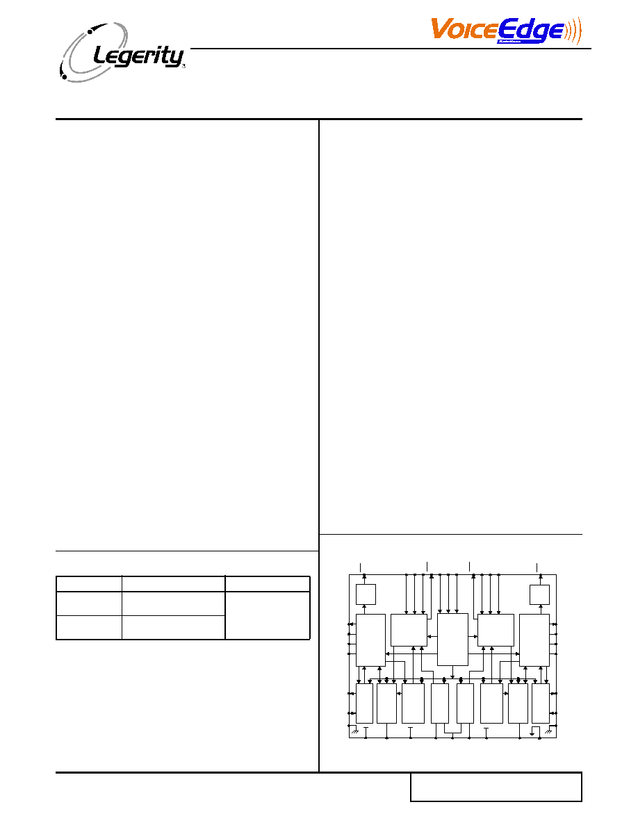
BLOCK DIAGRAM
BGND
1
AD
2
HP
2
BD
2
VTX
2
RSN
2
CH2
2-W
Interface
CH1
2-W
Interface
CH2
Input
Decoder
and Control
Common
Bias
Off-Hook &
Ground Start
Detector
CH2
Ring Trip
Detector
CH2
Ring Trip
Detector
CH1
Power Feed
Controller
CH1
Off-Hook &
Ground Start
Detector
CH1
Signal
Transmission
CH2
Signal
Transmission
CH1
CH1
Input
Decoder
and Control
CAS
IREF
AD
1
HP
1
BD
1
RSN
1
BGND
2
VBAT
CDC
2
DB
2
DAC
DB
1
CDC
1
VCC
AGND/
DGND
RD
C2
2
C1
2
C3
2
CH2
Fault
Detector
C2
1
C1
1
C3
1
CH1
Fault
Detector
TMG
2
TMG
1
Power Feed
Controller
CH2
VTX
1
120402
VBREF
DET
2
FLT
2
DET
1
FLT
1

2
Le5712 VE580 Series Data Sheet
Table of Contents
Applications . . . . . . . . . . . . . . . . . . . . . . . . . . . . . . . . . . . . . . . . . . . . . . . . . . . . . . . . . . . . . . . . . . . . . . .1
Features . . . . . . . . . . . . . . . . . . . . . . . . . . . . . . . . . . . . . . . . . . . . . . . . . . . . . . . . . . . . . . . . . . . . . . . . . .1
Ordering Information . . . . . . . . . . . . . . . . . . . . . . . . . . . . . . . . . . . . . . . . . . . . . . . . . . . . . . . . . . . . . . .1
Description. . . . . . . . . . . . . . . . . . . . . . . . . . . . . . . . . . . . . . . . . . . . . . . . . . . . . . . . . . . . . . . . . . . . . . . .1
Related Literature . . . . . . . . . . . . . . . . . . . . . . . . . . . . . . . . . . . . . . . . . . . . . . . . . . . . . . . . . . . . . . . . . .1
Block Diagram . . . . . . . . . . . . . . . . . . . . . . . . . . . . . . . . . . . . . . . . . . . . . . . . . . . . . . . . . . . . . . . . . . . . .1
Product Description . . . . . . . . . . . . . . . . . . . . . . . . . . . . . . . . . . . . . . . . . . . . . . . . . . . . . . . . . . . . . . . .3
Block Descriptions . . . . . . . . . . . . . . . . . . . . . . . . . . . . . . . . . . . . . . . . . . . . . . . . . . . . . . . . . . . . . . . . .3
Two-Wire Interface . . . . . . . . . . . . . . . . . . . . . . . . . . . . . . . . . . . . . . . . . . . . . . . . . . . . . . . . . . . . .3
Signal Transmission . . . . . . . . . . . . . . . . . . . . . . . . . . . . . . . . . . . . . . . . . . . . . . . . . . . . . . . . . . . .4
Power Feed Controller and Common Bias . . . . . . . . . . . . . . . . . . . . . . . . . . . . . . . . . . . . . . . . . . .4
Input Decoder and Control. . . . . . . . . . . . . . . . . . . . . . . . . . . . . . . . . . . . . . . . . . . . . . . . . . . . . . . .5
Device State Decoding . . . . . . . . . . . . . . . . . . . . . . . . . . . . . . . . . . . . . . . . . . . . . . . . . . . . . . . . . .5
Off-Hook Detector (OHD) . . . . . . . . . . . . . . . . . . . . . . . . . . . . . . . . . . . . . . . . . . . . . . . . . . . . . . . .5
Ground Start Detector (GSD) . . . . . . . . . . . . . . . . . . . . . . . . . . . . . . . . . . . . . . . . . . . . . . . . . . . . .5
Ring-Trip Detector . . . . . . . . . . . . . . . . . . . . . . . . . . . . . . . . . . . . . . . . . . . . . . . . . . . . . . . . . . . . . .5
Fault Detector . . . . . . . . . . . . . . . . . . . . . . . . . . . . . . . . . . . . . . . . . . . . . . . . . . . . . . . . . . . . . . . . .5
Thermal Shutdown. . . . . . . . . . . . . . . . . . . . . . . . . . . . . . . . . . . . . . . . . . . . . . . . . . . . . . . . . . . . . .6
Connection Diagram . . . . . . . . . . . . . . . . . . . . . . . . . . . . . . . . . . . . . . . . . . . . . . . . . . . . . . . . . . . . . . . .6
Pin Descriptions . . . . . . . . . . . . . . . . . . . . . . . . . . . . . . . . . . . . . . . . . . . . . . . . . . . . . . . . . . . . . . . . . . .7
Absolute Maximum Ratings . . . . . . . . . . . . . . . . . . . . . . . . . . . . . . . . . . . . . . . . . . . . . . . . . . . . . . . . . .8
Operating Ranges . . . . . . . . . . . . . . . . . . . . . . . . . . . . . . . . . . . . . . . . . . . . . . . . . . . . . . . . . . . . . . . . . .8
Environmental Ranges . . . . . . . . . . . . . . . . . . . . . . . . . . . . . . . . . . . . . . . . . . . . . . . . . . . . . . . . . .8
Electrical ranges . . . . . . . . . . . . . . . . . . . . . . . . . . . . . . . . . . . . . . . . . . . . . . . . . . . . . . . . . . . . . . .8
Electrical Characteristics . . . . . . . . . . . . . . . . . . . . . . . . . . . . . . . . . . . . . . . . . . . . . . . . . . . . . . . . . . . .9
Summary of Test Conditions . . . . . . . . . . . . . . . . . . . . . . . . . . . . . . . . . . . . . . . . . . . . . . . . . . . . . .9
Supply Currents and Power Dissipation (on-hook) . . . . . . . . . . . . . . . . . . . . . . . . . . . . . . . . . . . . .9
Specifications . . . . . . . . . . . . . . . . . . . . . . . . . . . . . . . . . . . . . . . . . . . . . . . . . . . . . . . . . . . . . . . . . . . . .9
Device specifications . . . . . . . . . . . . . . . . . . . . . . . . . . . . . . . . . . . . . . . . . . . . . . . . . . . . . . . . . . . .9
DC Feed Characteristics . . . . . . . . . . . . . . . . . . . . . . . . . . . . . . . . . . . . . . . . . . . . . . . . . . . . . . . .14
Test Circuits. . . . . . . . . . . . . . . . . . . . . . . . . . . . . . . . . . . . . . . . . . . . . . . . . . . . . . . . . . . . . . . . . .15
POTS Application Circuit (Battery-Backed Ringing) . . . . . . . . . . . . . . . . . . . . . . . . . . . . . . . . . . . . .18
Pulse Metering Application Circuit (Earth-Backed Ringing) . . . . . . . . . . . . . . . . . . . . . . . . . . . . . . .19
Application Circuit Parts List . . . . . . . . . . . . . . . . . . . . . . . . . . . . . . . . . . . . . . . . . . . . . . . . . . . . . . . .20
Physical Dimensions. . . . . . . . . . . . . . . . . . . . . . . . . . . . . . . . . . . . . . . . . . . . . . . . . . . . . . . . . . . . . . .21
Revision History . . . . . . . . . . . . . . . . . . . . . . . . . . . . . . . . . . . . . . . . . . . . . . . . . . . . . . . . . . . . . . . . . .22
Revision C1 to D1 . . . . . . . . . . . . . . . . . . . . . . . . . . . . . . . . . . . . . . . . . . . . . . . . . . . . . . . . . . . . .22
Revision D1 to E1 . . . . . . . . . . . . . . . . . . . . . . . . . . . . . . . . . . . . . . . . . . . . . . . . . . . . . . . . . . . . .22
Revision E1 to F1 . . . . . . . . . . . . . . . . . . . . . . . . . . . . . . . . . . . . . . . . . . . . . . . . . . . . . . . . . . . . .22

Le5712 VE580 Series Data Sheet
3
PRODUCT DESCRIPTION
The Le5712 device is designed for long loop high-density POTS applications requiring a low power, small footprint SLIC device.
The Le5712 device increases line card density by integrating two SLIC devices into a single 44-pin package. This reduction in
board space permits a higher density line card, which allows for amortizing common hardware across more channels. The
Le5712 device gives line card designers a simple control interface that supports seven states: Active, Active Metering, Reverse
Polarity, Reverse Polarity Metering, Standby, Tip Open and Disconnect (Ringing). The low cost and high performance Le5712
device provides the key features for POTS markets requiring loop start, loop start and metering, or ground start. The device
includes a thermal management feature for minimizing power dissipation on the SLIC. Alternatively, the device can be operated
in a dual battery configuration to reduce overall power consumption.
BLOCK DESCRIPTIONS
Two-Wire Interface
The two-wire interface provides DC current and sends voice and signalling information to a customer premise equipment. The
two-wire interface also receives the returning signals from the customer premise equipment.
This block implements the thermal management feature, which allows power that would otherwise be dissipated within the
package to be off loaded into an external resistor when the line is Off Hook. R
TMGi
is connected from TMG
i
to the VBAT pin and
limits power within the SLIC device (Note: "i" denotes channel number).
The minimum value of R
TMGi
is given by:
where I
LIMITMIN
is the minimum programmed loop current limit and R
LMIN
is the minimum loop resistance. The tolerance of R
TMG
should be taken into account when selecting a value that meets this requirement. For example, if BAT
MAX
= -56 V, I
LOOPMIN
= 30
mA and R
LMIN
= 200
then R
TMG
= 1.5 k
is the minimum recommended value. A value of 1.8 k with 5% accuracy will keep
the power in R
TMG
below 1.0 W, and the total worst case SLIC power dissipation with both channels active below 1.6 W.
The power dissipated in the TMG resistor is given by:
where I
L
is the loop current, and R
L
is the loop resistance.
The maximum power on R
TMG
is given by:
And the power dissipated per channel in the SLIC device while in the Active states is given by:
The maximum power dissipated per channel in the SLIC device while in the Active states is given by:
Refer to the Thermal Management for the Le5711 and Le7512 Dual SLIC Devices Application Note for further analysis and for
dual battery condition.
The AC signal swing supported by the two-wire interface is controlled by the SLIC state. For standard voice transmission, the
Active and Reverse Polarity states are used. To support voice plus meter pulses, the Active Metering and Reverse Polarity
Metering states are provided which have increased overhead to support 2.0 Vrms metering.
R
TMG
BAT
MAX
6
�
I
LIMITMIN
2 R
F
�
R
LMIN
40
+
+
(
)
�
I
LIMITMIN
3 mA
�
----------------------------------------------------------------------------------------------------------------------------------
P
RTMG
BAT
5
�
I
L
� R
L
2R
F
40
+
+
(
)
�
(
)
2
R
TMG
-------------------------------------------------------------------------------------------
=
P
RTMGmax
BAT
max
5
�
I
LIMITmin
R
Lmin
2R
F
40
+
+
(
)
�
(
)
2
R
TMGmin
---------------------------------------------------------------------------------------------------------------------------
=
P
SLICi
0.003 BAT
BAT
3
�
I
L
R
L
2R
F
40
+
+
(
)
�
(
) I
L
I
R
TMG
--------------- BAT
5
�
I
L
R
L
2R
F
40
+
+
(
)
�
(
)
�
+
=
P
SLICmaxi
0.003 BAT
max
1
I
LIMITmax
2
-------------------------R
TMGmax
+
I
LIMITmax
2
-------------------------
1
R
TMGmax
------------------------
+
+
=

4
Le5712 VE580 Series Data Sheet
Signal Transmission
The RSN
i
input current controls the receive current sent to the two-wire interface. The AC line voltage is sensed by a differential
amplifier between the AD
i
and HP
i
leads. The output of this amplifier is equal to the AC metallic components of the line voltages
and is output at VTX
i
.
The desired two-wire AC input impedance, Z
2WIN
, is defined by the fuse resistors, R
F
, and an impedance connected from VTX
i
to RSN
i
, Z
Ti
. When computing Z
Ti
, the internal current amplifier pole and any external stray capacitance between VTX and RSN
must be taken into account.
To set the desired receive gain (G
42L
) into a load Z
L
from VRX
i
, Z
RXi
is connected from VRX
i
to RSN
i
, where
The transmission block also contains a longitudinal feedback circuit to shunt longitudinal signals to a DC bias voltage. The
longitudinal feedback does not affect metallic signals.
Two application circuits, provided at the end of this data sheet, show how the Le5712 device can connect directly to pins of a
QLSLAC codec.
The
POTS Application Circuit (Battery-Backed Ringing),
on page 18
shows an application providing Loop Start and Ground
Start capability. The components selected for the transmission network allow a wide range of market transmission requirements
to be met when combined with the programmable QLSLAC device. In addition, transmit relative levels of Li = +4 to -4 dBr and
receive relative levels of Lo = 0 to -8dBr can be supported using only the digital gain within the QLSLAC device for all markets.
This configuration will meet ITU Q.552 and GR57 requirements.
The
Pulse Metering Application Circuit (Earth-Backed Ringing),
on page 19
shows a configuration for use in a 12 or 16
kHz pulse metering application with the QLSLAC device. The design allows 2 Vrms into 200
, and supports gain ranges of at
least Li = 0 to +4dBr, and Lo = 0 to -8 dBr. This configuration will meet ITU Q.552 requirements over these gain ranges for markets
such as India and China.
The relationship between metering source V
M
, the feeding resistance, R
M
, and the output voltage at tip-ring, V
TR
, is given in the
following equation. The load at tip-ring is R
M
. R
F
is the protection and other, if any, front-end resistances. Z
T
is the impedance
between VTX and RSN at metering frequency.
Metering signal at VTX needs to be filtered to prevent from overloading the codec. This has been realized in the applications
circuitry in this document.
Power Feed Controller and Common Bias
The power feed controllers have three sections: (1) the common bias circuit, (2) the battery feed circuit, and (3) the reverse
polarity circuit which operate in all Active states.
The bias circuit provides a signal which sets the current limit and creates a voltage related to V
BAT
, filtered by a capacitor
connected to the CAS pin, to the battery feed circuit.
The nominal current limit is set by the following equation:
A recommended 3 Hz filter pole frequency (f
c
) can be implemented from:
The battery feed circuit regulates the amount of DC current and voltage supplied to the telephone over a wide range of loop
resistance. It is designed to operate over a nominal 22 to 33 mA range of programmed current limit. It produces a filtered
reference voltage offset from the subscriber line voltage which is applied to the two-wire interface.
In addition, a low pass filter is implemented with a capacitor connected to the CDC
i
pin.
In the low power Standby state, an alternative feed is implemented via two current limited on chip 200-
resistors. The nominal
loop current below current limit in the Standby state is given by:
Z
Ti
500
3
---------
Z
2WIN
2R
F
�
(
)
=
Z
RXi
Z
L
G
42L
-------------
500 Z
T
�
Z
T
500
3
--------- Z
L
2R
F
+
(
)
+
---------------------------------------------------
�
=
V
TR
Z
M
R
M
--------
=
500
1
500
3
---------
Z
M
2R
F
+
Z
T
------------------------
�
+
-------------------------------------------------
�
V
M
I
LIMIT
470
R
REF
--------------
=
C
CAS
1
RI
AS
2
�
f
c
�
�
-----------------------------------------
=
I
STANDBY
V
BAT
4 V
�
600
R
L
+
--------------------------------
=
Le5712 VE580 Series Data Sheet
5
Input Decoder and Control
The input decoder and control block provides a means for a microprocessor or SLAC device IC to control such system states as
Active, Active Metering, Reverse Polarity, Reverse Polarity Metering, Standby, Tip Open and Disconnect (Ringing). The input
decoder and control block has TTL-compatible inputs, permitting interfacing to 5 or 3.3 V VCC controllers which set the operating
states of the SLIC device. It also provides the loop supervision signal sent back to the controller.
From power up, the device is in disconnect state unless over-written by external control inputs.
Reverse Polarity states 3 and 7 are not available on the Le57123/124 devices.
Device State Decoding
(For channel i = 1 or 2)
Off-Hook Detector (OHD)
The On-to-Off-hook and Off-to-On-hook detections are based on loop current and are defined as |I
AD
- I
BD
| / 2. The On-to-Off-
hook (OHD) and Off-to-On-hook (OND) thresholds are programmed with the R
D
resistor and the threshold applies to all Active
and Standby states.
Upon the loss of battery the DET pin will be HIGH.
Off-hook detection or DET state should be ignored during on-hook metering.
Ground Start Detector (GSD)
This detector is active in the Tip Open state. The threshold, I
GSD
, is defined by the same equation used for the OHD.
For ground start lines, the device is in the Tip Open state between calls. When a ring ground condition is detected, the device
should be switched to the Active state. During this period, the DET pin will be active if the ring to ground current is greater than
twice the I
OHD
threshold. The DET pin will go active once the ring ground is removed and a loop is applied. It is recommended
that a firmware time-out period is applied in case the call attempt is abandoned and DET never goes low. The time-out is reset
once an active DET is seen in the Active state.
Ring-Trip Detector
In the Disconnect state, the ring-trip detector is active. While the DB
i
pin is more negative than the DAC pin, the DET pin will be
High to indicate on hook. When an off hook condition occurs, the DB
i
pin becomes more positive than the DAC pin, and the DET
pin will go Low to indicate off hook during ringing (ring-trip) has been detected. The system implements the Ringing state using
external control of a ring relay in combination with the Disconnect SLIC device state, which enables the ring-trip detector.
The
POTS Application Circuit (Battery-Backed Ringing),
on page 18
shows a ring trip bridge configured and components
are selected for a typical battery-backed ringing applications such as for the US (TR-57) and China (GF002).
The
Pulse Metering Application Circuit (Earth-Backed Ringing),
on page 19
shows a ring trip bridge configured and
components are selected for a typical earth-backed ringing applications such as in India (G/LLT and G/MLT).
Fault Detector
The DSLIC device provides a fault detection function in the Active states on each channel. Under a fault condition the detector
senses longitudinal voltage at tip and ring and flags a fault by pulling the FLT
i
pin Low. The FLT
i
pins are compatible with logic
inputs, and may be monitored to clearly identify a fault condition from a loop condition. However, these outputs only have low
current drive.
State
C3
i
C2
i
C1
i
Two-Wire state
DET
i
output
0
0
0
0
Reserved
N/A
1
0
0
1
Active Metering
OHD
2
0
1
0
Tip Open
GSD
3
0
1
1
Reverse Polarity Metering
OHD
4
1
0
0
Disconnect
RTD
5
1
0
1
Active
OHD
6
1
1
0
Standby
OHD
7
1
1
1
Reverse Polarity
OHD
I
OHD
935V
R
D
-------------
=
I
OHD
I
OND
Hysteresis
+
=