Document ID# 081189
Date:
Oct 12, 2006
Rev:
G
Version: 1
Distribution:
Public Document
TM
Le9500
High-Voltage Ringing SLIC Device for VolP Applications
VE950 Series
APPLICATIONS
Interface to Broadcom:
-- BCM3367/3368 cable modem
-- BCM3341/3351/3352 cable modem
-- BCM6352 integrated multimedia adaptor
-- BCM1101 residential gateway
Cable modems
Voice over Internet Protocol (VoIP)
Voice over DSL
Remote subscriber units
Broadband wireless
Short-loop access
FEATURES
Differential ringing and codec interface
Single-ended application also supported
On-board ringing generation
-- 15 to 70 Hz ring frequency supported
Three ringing options:
-- Sine wave input - sine wave output
-- PWM input - sine wave output
-- Square wave input - trapezoidal output
Flexible power supply options:
-- V
BAT2
for active talking
-- V
BAT1
for ringing, scan, and so on
-- 3.3 V for V
CC
Battery switch to minimize off-hook power
Eight operating states:
-- Scan
-- Forward and reverse battery active
-- Forward and reverse battery on-hook transmission
-- Ground start
-- Ring
-- Disconnect
Ultra-low on-hook power:
-- 29 mW scan state
-- 38 mW active state
Loop start, ring trip, and ground start detection
-- Fixed off hook threshold with hysteresis
-- Fixed ground start threshold with hysteresis
-- Fixed ring-trip threshold as a function of battery voltage
Software-controllable dual-current limit option
-- 25 mA or 40mA via ground or open control input
UL1950 Compatible
-- When not in ringing, |V
TIP
| and |V
RING
| are clamped to
be less than 56.5 V
Thermal shutdown protection with hysteresis
28-pin PLCC package
HV7 Technology
ORDERING INFORMATION
1.
The green package meets RoHS Directive 2002/95/EC of the
European Council to minimize the environmental impact of
electrical equipment.
2.
For delivery using a tape and reel packing system, add a "T" suffix
to the OPN (Ordering Part Number) when placing an order.
Device
Package Type
1
Packing
2
Le9500ABJC
28-Pin PLCC, -75V (Green)
Tube
Le9500BBJC
28-Pin PLCC, -85V (Green)
Le9500CBJC
28-Pin PLCC, -100V (Green)
Le9500DBJC
28-Pin PLCC, -100V
operation / -145V ringing
(Green)
DESCRIPTION
The Legerity Le9500 device, part of the VE950 series, is a
subscriber line interface circuit (SLIC) that is optimized for
short-loop, power-sensitive applications. This device provides
the complete set of line interface functionality (including power
ringing) needed to interface to a subscriber loop while
providing ultra low power dissipation. The Le9500 SLIC device
is capable of operating with a V
CC
supply of 3.3 V, and is
designed to minimize external components required at all
device interfaces. The differential ringing and receive inputs
make the device ideal for direct interface to Data Over Cable
Service Interface Specification (DOCSIS) compliant cable
modem gateways, to multimedia adaptors, and to residential
gateway products, such as the Broadcom� BCM3367/3368,
BCM3341/3351/3352, BCM6353, BCM1101 and equivalent
products.
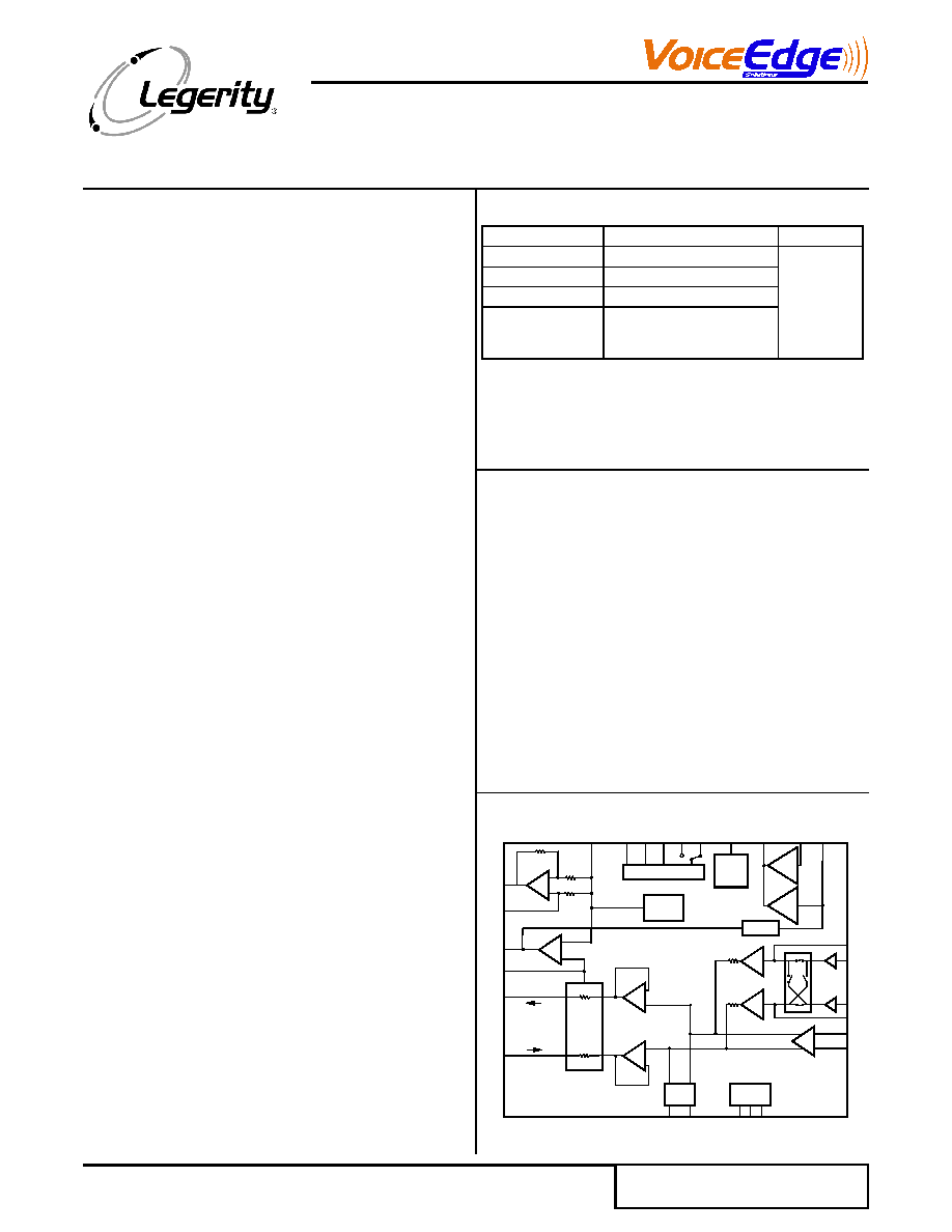
BLOCK DIAGRAM
V
REF
VITR
TXI
ITR
VTX
PT
PR
CF2
CF1
FB2
FB1
POWER
AGND
V
CC
BGND V
BAT2
V
BAT1
V
PROG
NSTAT
RTFLT
DCOUT
1.5 V
BAND-GAP
REFERENCE
GAIN = 20
(ITR/306)
TIP/RING
CURRENT
SENSE
AT
RFT
18
RFR
18
AR
RINGING
GAIN = 65
PARALLEL
DATA
INTERFACE
RING
INN
B0 B1 B2
X1
X1
RCVP
RCVN
CURRENT
LIMIT
AND
INRUSH
CONTROL
RING
LOOP
RECTIFIER
TRIP
CLOSURE
�
+
+
�
+
�
�
+
AX
AC
RING
INP
GAIN = 4
AAC

P R E L I M I N A R Y
2
Le9500 VE950 Series Data Sheet
TABLE OF CONTENTS
Applications . . . . . . . . . . . . . . . . . . . . . . . . . . . . . . . . . . . . . . . . . . . . . . . . . . . . . . . . . . . . . . . . . . . . . . .1
Features . . . . . . . . . . . . . . . . . . . . . . . . . . . . . . . . . . . . . . . . . . . . . . . . . . . . . . . . . . . . . . . . . . . . . . . . . .1
Ordering Information . . . . . . . . . . . . . . . . . . . . . . . . . . . . . . . . . . . . . . . . . . . . . . . . . . . . . . . . . . . . . . .1
Description. . . . . . . . . . . . . . . . . . . . . . . . . . . . . . . . . . . . . . . . . . . . . . . . . . . . . . . . . . . . . . . . . . . . . . . .1
Block Diagram . . . . . . . . . . . . . . . . . . . . . . . . . . . . . . . . . . . . . . . . . . . . . . . . . . . . . . . . . . . . . . . . . . . .1
Table of Contents . . . . . . . . . . . . . . . . . . . . . . . . . . . . . . . . . . . . . . . . . . . . . . . . . . . . . . . . . . . . . . . . . .2
Product Description . . . . . . . . . . . . . . . . . . . . . . . . . . . . . . . . . . . . . . . . . . . . . . . . . . . . . . . . . . . . . . . .3
Connection Diagram . . . . . . . . . . . . . . . . . . . . . . . . . . . . . . . . . . . . . . . . . . . . . . . . . . . . . . . . . . . . . . . .4
Pin Descriptions . . . . . . . . . . . . . . . . . . . . . . . . . . . . . . . . . . . . . . . . . . . . . . . . . . . . . . . . . . . . . . . . . . .5
Absolute Maximum Ratings . . . . . . . . . . . . . . . . . . . . . . . . . . . . . . . . . . . . . . . . . . . . . . . . . . . . . . . . . .6
Operating Ranges . . . . . . . . . . . . . . . . . . . . . . . . . . . . . . . . . . . . . . . . . . . . . . . . . . . . . . . . . . . . . . . . . .6
Electrical Characteristics . . . . . . . . . . . . . . . . . . . . . . . . . . . . . . . . . . . . . . . . . . . . . . . . . . . . . . . . . . . .7
Supply Currents . . . . . . . . . . . . . . . . . . . . . . . . . . . . . . . . . . . . . . . . . . . . . . . . . . . . . . . . . . . . . . . .7
Power Dissipation . . . . . . . . . . . . . . . . . . . . . . . . . . . . . . . . . . . . . . . . . . . . . . . . . . . . . . . . . . . . . .8
Line Characteristics . . . . . . . . . . . . . . . . . . . . . . . . . . . . . . . . . . . . . . . . . . . . . . . . . . . . . . . . . . . . . . . .9
Operating States . . . . . . . . . . . . . . . . . . . . . . . . . . . . . . . . . . . . . . . . . . . . . . . . . . . . . . . . . . . . . . . . . .12
Operating State Definitions . . . . . . . . . . . . . . . . . . . . . . . . . . . . . . . . . . . . . . . . . . . . . . . . . . . . . .12
Test Circuit. . . . . . . . . . . . . . . . . . . . . . . . . . . . . . . . . . . . . . . . . . . . . . . . . . . . . . . . . . . . . . . . . . . . . . .14
Applications . . . . . . . . . . . . . . . . . . . . . . . . . . . . . . . . . . . . . . . . . . . . . . . . . . . . . . . . . . . . . . . . . . . . . .16
DC Loop Current Limit . . . . . . . . . . . . . . . . . . . . . . . . . . . . . . . . . . . . . . . . . . . . . . . . . . . . . . . . . .16
Overhead Voltage . . . . . . . . . . . . . . . . . . . . . . . . . . . . . . . . . . . . . . . . . . . . . . . . . . . . . . . . . . . . .16
DC Loop Range . . . . . . . . . . . . . . . . . . . . . . . . . . . . . . . . . . . . . . . . . . . . . . . . . . . . . . . . . . . . . . .16
Battery Reversal Rate . . . . . . . . . . . . . . . . . . . . . . . . . . . . . . . . . . . . . . . . . . . . . . . . . . . . . . . . . .17
Supervision . . . . . . . . . . . . . . . . . . . . . . . . . . . . . . . . . . . . . . . . . . . . . . . . . . . . . . . . . . . . . . . . . .17
Power Ring . . . . . . . . . . . . . . . . . . . . . . . . . . . . . . . . . . . . . . . . . . . . . . . . . . . . . . . . . . . . . . . . . .17
Design Examples. . . . . . . . . . . . . . . . . . . . . . . . . . . . . . . . . . . . . . . . . . . . . . . . . . . . . . . . . . . . . .19
Physical Dimensions . . . . . . . . . . . . . . . . . . . . . . . . . . . . . . . . . . . . . . . . . . . . . . . . . . . . . . . . . . . . . .23
Revision History . . . . . . . . . . . . . . . . . . . . . . . . . . . . . . . . . . . . . . . . . . . . . . . . . . . . . . . . . . . . . . . . . .24
Revision A1 to B1 . . . . . . . . . . . . . . . . . . . . . . . . . . . . . . . . . . . . . . . . . . . . . . . . . . . . . . . . . . . . .24
Revision B1 to C1 . . . . . . . . . . . . . . . . . . . . . . . . . . . . . . . . . . . . . . . . . . . . . . . . . . . . . . . . . . . . .24
Revision C1 to D1 . . . . . . . . . . . . . . . . . . . . . . . . . . . . . . . . . . . . . . . . . . . . . . . . . . . . . . . . . . . . .24
Revision D1 to E1 . . . . . . . . . . . . . . . . . . . . . . . . . . . . . . . . . . . . . . . . . . . . . . . . . . . . . . . . . . . . .24
Revision E1 to F1 . . . . . . . . . . . . . . . . . . . . . . . . . . . . . . . . . . . . . . . . . . . . . . . . . . . . . . . . . . . . .24
Revision F1 to F2. . . . . . . . . . . . . . . . . . . . . . . . . . . . . . . . . . . . . . . . . . . . . . . . . . . . . . . . . . . . . .24
Revision F2 to G1 . . . . . . . . . . . . . . . . . . . . . . . . . . . . . . . . . . . . . . . . . . . . . . . . . . . . . . . . . . . . .24

P R E L I M I N A R Y
Le9500 VE950 Series Data Sheet
3
PRODUCT DESCRIPTION
The Le9500 device is optimized to provide battery feed, ringing, and supervision on short Plain Old Telephone Service (POTS)
loops. This device provides power ringing to the subscriber loop through amplification of a low-voltage input. It also provides
forward and reverse battery feed states, on-hook transmission, a low-power scan state, ground start (tip open), and a forward
disconnect state.
The Le9500 device requires a 3.3V V
CC
and battery to operate eight operating states. A battery switch is included to allow for
use of a lower-voltage battery in the off-hook condition, thus minimizing short-loop off-hook power.
The following two batteries are used:
1. A high-voltage operation and ringing battery (V
BAT1
):
V
BAT1
is used for scan, on-hook transmission, ground start, and power ringing. It can be a maximum of �75 V for Le9500A,
�85 V for Le9500B, or �100V for Le9500C and Le9500D.
For Le9500D during ringing only this voltage may be extended to �145 V. The supply has to be externally adjustable. It has
to be adjusted back to no more than -100 V for other operation states. Further, when �145 V is used for ringing special care
should be applied to prevent certain faults from happening such as tip to ring, tip or ring to ground.
2. A lower-voltage talk battery (V
BAT2
):
V
BAT2
is used for active state powering.
Loop closure, ring trip, and ground start detection is available. The loop closure detector has fixed threshold with hysteresis. The
ring trip detector requires a single-pole filter, thus minimizing external components required. The ring trip threshold at a given
battery voltage is fixed and with hysteresis. Ground start detection also has fixed threshold with hysteresis.
The DC current limit is set and fixed by a logic-controllable pin. Ground or open applied to this pin sets the current limit at the low
or high value.
This device is designed for ultra-low power in all operating states.
Forward and reverse battery active states are used for off-hook conditions. Since this device is designed for short-loop
applications, the lower-voltage V
BAT2
is applied during the forward and reverse active states
.
Battery reversal is quiet, without
breaking the AC path. Rate of battery reversal may be ramped to control switching time.
The magnitude of the overhead voltage in the forward and reverse active states has a typical default value of 7.2 V, allowing for
an on-hook transmission of an undistorted signal of 3.14 dBm into 900
. Additionally, this allows sufficient overhead for 500 mV
of meter pulse if desired. This overhead is fixed. The ring trip detector is turned off during active states to conserve power.
Because on-hook transmission is not allowed in the scan state, an on-hook transmission state is defined. This state is functionally
similar to the active state, except the tip ring voltage is derived from the higher V
BAT1
rather than V
BAT2
.
In the on-hook transmission states with a primary battery whose magnitude is greater than a nominal 56.5 V, the magnitude of
the tip-to-ground and ring-to-ground voltage is clamped at less than 56.5 V.
To minimize on-hook power, a low-power scan state is available. In this state, all functions except off-hook supervision are turned
off to conserve power. On-hook transmission is not allowed in the scan state.
In the scan state with a primary battery whose magnitude is greater than a nominal 56.5 V, the magnitude of the tip-to-ground
and ring-to-ground voltage is clamped at less than 56.5 V.
A forward disconnect state is provided, where all circuits are turned off and power is denied to the loop.
The device offers a ring state, in which a power ring signal is provided to the tip/ring pair. During the ring state, user-supplied low-
voltage ring signals are input to the device's RING
INP/N
inputs. The input signals can be differential or single-ended, and can
either or both include certain DC offset. Both inputs should reference to Vref. The two signals are amplified to produce the power
ring signal. The input signal or signals may be a sine wave or filtered square wave to produce a sine wave or trapezoidal output.
The Ring Trip detector is active during the ring state. The flexibility makes the device ideal to directly interface to DOCSIS
compliant cable modem gateway products.
This feature eliminates the need for a separate external ring relay, associated external circuitry, and a bulk ringing generator.
The device offers a ground start state. In this state, the tip drive amplifier is turned off. The device presents a high impedance
(>100 k
) to PT and a current-limited battery (V
BAT1
) to PR. The voltage on PR is clamped to be less than 56.5 V in magnitude.
The NSTAT loop current detector is used for ring ground detection. In the ground start state, since the loop current is common
state, the loop closure threshold is reduced in half, thus maintaining loop supervision at specified levels.
Upon reaching the thermal shutdown temperature, the device will enter an all off state. Upon cooling, the device will re-enter the
state it was in prior to thermal shutdown. Hysteresis is built in to prevent oscillation.
Data control is via a parallel unlatched control scheme.
Circuitry is added to the Le9500 device to minimize the inrush of current from the V
CC
supply and to the battery supply during an
on- to off-hook transition, thus saving in power supply design cost.
P R E L I M I N A R Y
4
Le9500 VE950 Series Data Sheet
The Le9500 device uses a voltage feed-current sense architecture. The transmit gain is a transimpedance. The Le9500 device
transimpedance is set via a single external resistor, and this device is designed for optimal performance with a transimpedance
set at 300 V/A. This interface is single ended. The Le9500 device offers a differential receive interface with a gain of 8.
The Le9500 device is internally referenced to 1.5 V. This reference voltage is output at the V
REF
pin of the device. The VITR output
is also referenced to 1.5 V. The RCVP/RCVN
receive inputs are floating inputs.
The Le9500 device is available in a 28-pin PLCC package.
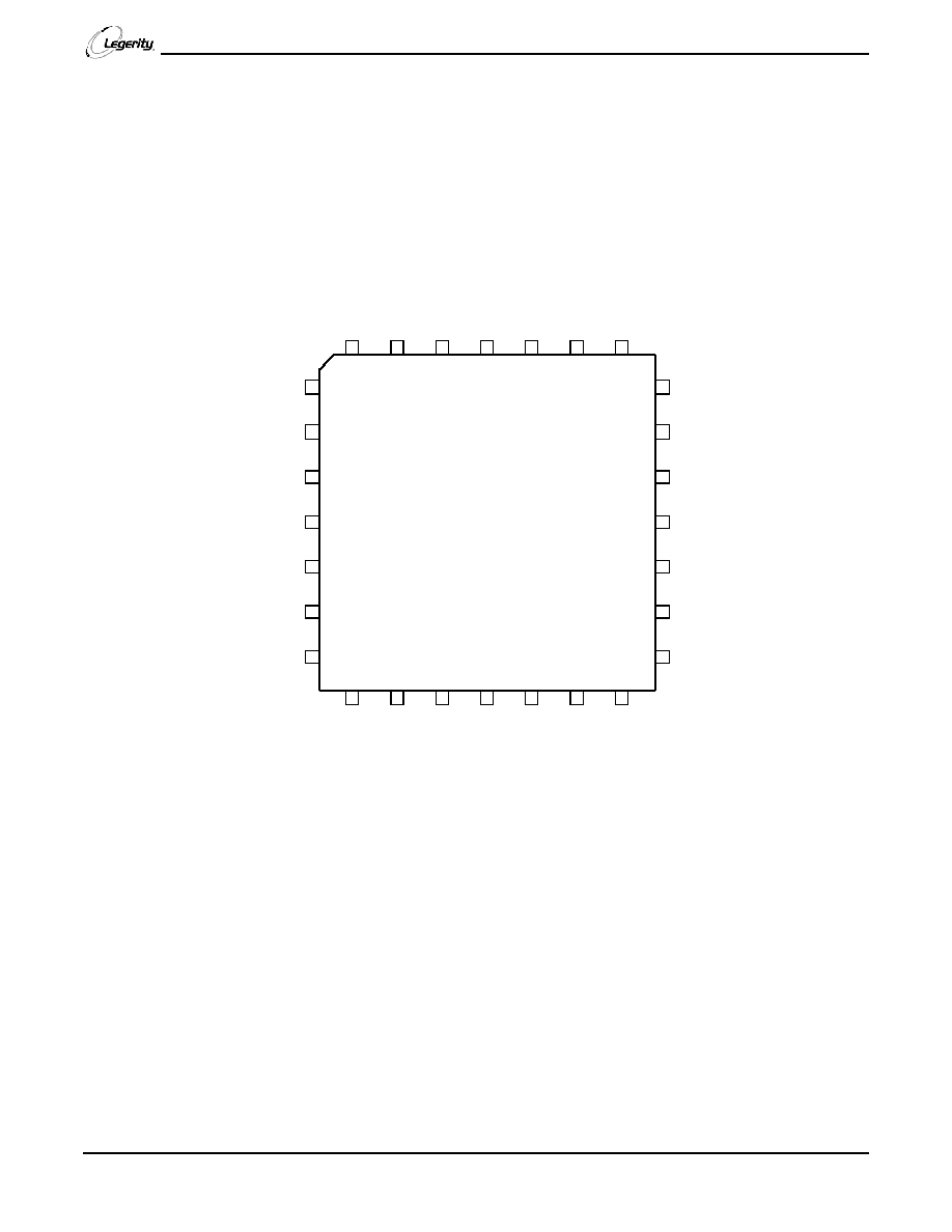
CONNECTION DIAGRAM
Figure 1. Le9500 28-Pin PLCC Connection Diagram
B0
B1
B2
PR
PT
FB1
RING
INP
CF2
CF1
RTFLT
5
6
7
8
9
10
11
4
2
1
28
27
3
12
14
15
16
17
18
13
25
24
23
22
21
20
19
NSTAT
V
BA
T
2
AG
ND
V
PR
OG
NC
V
BA
T
1
V
CC
BG
ND
DCOUT
RING
INN
V
REF
FB2
VTX
TXI
VITR
RCVP
RCVN
26
ITR
28-PIN PLCC

P R E L I M I N A R Y
Le9500 VE950 Series Data Sheet
5
PIN DESCRIPTIONS
Pin Name
Type
Description
NSTAT
Output
Loop Closure Detector Output--Ring Trip Detector Output. When Low, this logic output indicates that
an off-hook condition exists or ringing is tripped or a ring ground has occurred.
VITR
Output
Transmit AC Output Voltage. Output of internal AAC amplifier. This output is a voltage that is directly
proportional to the differential AC tip/ring current.
RCVP
Input
Receive AC Signal Input (Non inverting). This high-impedance input controls to AC differential voltage
on tip and ring. This node is a floating input.
RCVN
Input
Receive AC Signal Input (Inverting). This high-impedance input controls to AC differential voltage on tip
and ring. This node is a floating input.
RING
INN
Input
Power Ring Signal Input. Couple to a sine wave or lower crest factor low-voltage ring signal. The input
here is amplified to provide the full power ring signal at tip and ring. This signal may be applied
continuously, even during nonringing states.
RING
INP
Input
Power Ring Signal Input. Couple to a sine wave or lower crest factor low-voltage ring signal. The input
here is amplified to provide the full power ring signal at tip and ring. This signal may be applied
continuously, even during nonringing states.
DCOUT
Output
DC Output Voltage. This output is a voltage that is directly proportional to the absolute value of the
differential tip/ring current. This is used to set ring trip threshold.
CF2
--
Filter Capacitor. Connect a capacitor from this node to ground.
CF1
--
Filter Capacitor. Connect a capacitor from this node to CF2.
RTFLT
--
Ring Trip Filter. Connect this lead to DCOUT via a resistor and to AGND with a capacitor to filter the ring
trip circuit to prevent spurious responses. A single-pole filter is needed.
V
REF
Output
SLIC Device Internal Reference Voltage. Output of internal 1.5 V reference voltage.
AGND
Ground
Analog Signal Ground.
V
CC
Power
Analog Power Supply. 3.3 V typical.
V
BAT1
Power
Battery Supply 1. High-voltage battery.
V
BAT2
Power
Battery Supply 2. Lower-voltage battery.
BGND
Ground
Battery Ground. Ground return for the battery supplies.
NC
--
No Connection.
V
PROG
Input
Current-Limit Program Input. Connect this pin to ground to set current limit to 25 mA; leave this pin open
to set current limit to 40 mA.
FB2
--
Polarity Reversal Slowdown Capacitor. Connect a capacitor from this node for controlling rate of battery
reversal. If ramped battery reversal is not desired, leave this pin floating.
FB1
--
Polarity Reversal Slowdown Capacitor. Connect a capacitor from this node for controlling rate of battery
reversal. If ramped battery reversal is not desired, leave this pin floating.
PT
I/O
Protected Tip. The output drive of the tip amplifier and input to the loop-sensing circuit. Connect to loop
through overvoltage and overcurrent protection.
PR
I/O
Protected Ring. The output drive of the ring amplifier and input to the loop sensing circuit. Connect to
loop through overvoltage and overcurrent protection.
B2
Input
State Control Input. These pins have an internal 150 k
pull-up.
B1
Input
State Control Input. These pins have an internal 150 k
pull-up.
B0
Input
State Control Input. These pins have an internal 150 k
pull-up.
ITR
Input
Transmit Gain. Input to AX amplifier. Connect a 4.75 k
resistor from this node to VTX to set transmit
gain. Gain shaping for termination impedance with a first-generation codec is also achieved with a network
from this node to VTX.
VTX
Output
AC Output Voltage. Output of internal AX amplifier. The voltage at this pin is directly proportional to the
differential tip/ring current.
TXI
Input
AC/DC Separation. Input to internal AAC amplifier. Connect a capacitor from this pin to VTX.