 | –≠–ª–µ–∫—Ç—Ä–æ–Ω–Ω—ã–π –∫–æ–º–ø–æ–Ω–µ–Ω—Ç: DCR490J65 | –°–∫–∞—á–∞—Ç—å:  PDF PDF  ZIP ZIP |

1/9
www.dynexsemi.com
FEATURES
∑
Double Side Cooling
∑
High Surge Capability
APPLICATIONS
∑
High Power Drives
∑
High Voltage Power Supplies
∑
Static Switches
VOLTAGE RATINGS
Part and
Ordering
Number
Repetitive Peak
Voltages
V
DRM
and V
RRM
V
Conditions
DCR490J65
DCR490J62
DCR490J58
6500
6200
5800
T
vj
= -40∞ C to 125∞ C,
I
DRM
= I
RRM
= 100mA,
V
DRM
, V
RRM
t
p
= 10ms,
V
DSM
& V
RSM
=
V
DRM
& V
RRM
+ 100V
respectively
Lower voltage grades available.
ORDERING INFORMATION
When ordering, select the required part number
shown in the Voltage Ratings selection table.
For example:
DCR490J65
Note: Please use the complete part number when ordering
and quote this number in any future correspondence
relating to your order.
KEY PARAMETERS
V
DRM
6500V
I
T(AV)
490A
I
TSM
6600A
dV/dt*
1500V/µs
dI/dt
200A/us
* Higher dV/dt selections available
Outline type code: J
(See Package Details for further information)
Fig. 1 Package outline
DCR490J65
Phase Control Thyristor
Preliminary Information
DS5830-1.0 February 2005 (LN23801)

SEMICONDUCTOR
DCR
490
J65
2/9
www.dynexsemi.com
CURRENT RATINGS
T
case
= 60∞ C unless stated otherwise
Symbol
Parameter
Test Conditions
Max.
Units
Double Side Cooled
I
T(AV)
Mean on-state current
Half wave resistive load
490
A
I
T(RMS)
RMS value
-
770
A
I
T
Continuous (direct) on-state current
-
730
A
SURGE RATINGS
Symbol
Parameter
Test Conditions
Max.
Units
I
TSM
Surge (non-repetitive) on-state current
10ms half sine, T
case
= 125∞ C
6.6
kA
I
2
t
I
2
t for fusing
V
R
= 0
0.22
MA
2
s
THERMAL AND MECHANICAL RATINGS
Symbol
Parameter
Test Conditions
Min.
Max.
Units
R
th(j-c)
Thermal resistance ≠ junction to case
Double side cooled
DC
-
0.0379
∞ C/W
Single side cooled
Anode DC
-
0.0745
∞ C/W
Cathode DC
-
0.0797
∞ C/W
R
th(c-h)
Thermal resistance ≠ case to heatsink
Clamping force 11.5kN
Double side
-
0.0072
∞ C/W
(with mounting compound)
Single side
-
.0144
∞ C/W
T
vj
Virtual junction temperature
On-state (conducting)
-
135
∞ C
Reverse (blocking)
-
125
∞ C
T
stg
Storage temperature range
-55
125
∞ C
F
m
Clamping force
10
13
kN
SEMICONDUCTOR
DCR
490
J65
3/9
www.dynexsemi.com
DYNAMIC CHARACTERISTICS
Symbol
Parameter
Test Conditions
Min.
Max.
Units
I
RRM
/I
DRM
Peak reverse and off-state current
At V
RRM
/V
DRM
, T
case
= 125∞ C
-
100
mA
dV/dt
Max. linear rate of rise of off-state voltage
To 67% V
DRM
, T
j
= 125∞ C, gate open
-
1500
V/µs
dI/dt
Rate of rise of on-state current
From 67% V
DRM
to 2x I
T(AV)
Repetitive 50Hz
-
100
A/µs
Gate source 30V, 10
,
Non-repetitive
-
200
A/µs
t
r
< 0.5µs, T
j
= 125∞ C
V
T(TO)
Threshold voltage ≠ Low level
50A to 400A at T
case
= 125∞ C
-
0.912
V
Threshold voltage ≠ High level
400A to 1600A at T
case
= 125∞ C
-
1.108
V
r
T
On-state slope resistance ≠ Low level
50A to 400A at T
case
= 125∞ C
-
2.157
m
On-state slope resistance ≠ High level
400A to 1600A at T
case
= 125∞ C
-
1.647
m
t
gd
Delay time
V
D
= 67% V
DRM
, gate source 30V, 10
TBD
TBD
µs
t
r
= 0.5µs, T
j
= 25∞ C
t
q
Turn-off time
T
j
= 125∞ C, V
R
= 200V, dI/dt = 5A/µs,
750
1600
µs
dV
DR
/dt = 20V/µs linear
Q
S
Stored charge
I
T
= 2000A, T
j
= 125∞ C, dI/dt = 5A/µs,
1600
2600
µC
I
L
Latching current
T
j
= 25∞ C, V
D
= 5V
TBD
TBD
mA
I
H
Holding current
T
j
= 25∞ C, R
G-K
=
, I
TM
= 500A, I
T
= 5A
TBD
TBD
mA
SEMICONDUCTOR
DCR
490
J65
4/9
www.dynexsemi.com
GATE TRIGGER CHARACTERISTICS AND RATINGS
Symbol
Parameter
Test Conditions
Max.
Units
V
GT
Gate trigger voltage
V
DRM
= 5V, T
case
= 25∞ C
1.5
V
V
GD
Gate non-trigger voltage
At V
DRM,
T
case
= 125∞ C
TBD
V
I
GT
Gate trigger current
V
DRM
= 5V, T
case
= 25∞ C
250
mA
I
GD
Gate non-trigger current
V
DRM
= 5V, T
case
= 25∞ C
TBD
mA
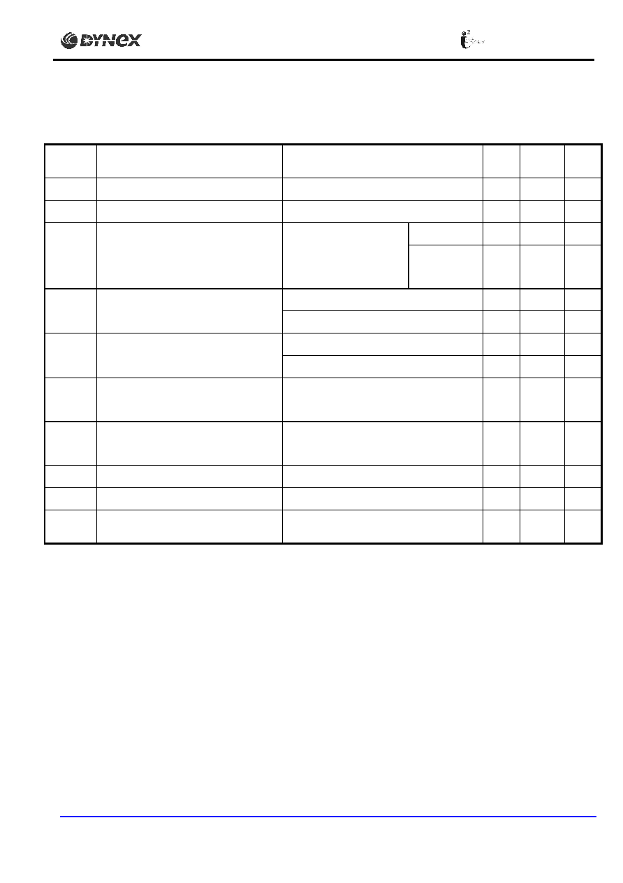
CURVES
0
400
800
1200
1600
1.0
2.0
3.0
4.0
Instantaneous on-state voltage, V
T
- (V)
Instantaneous on-state current, I
T
- (A)
25∞ C min
25∞ C max
125∞ C min
125∞ C max
Fig.2 Maximum & minimum on-state characteristics
V
TM
EQUATION
Where
A = 0.542452
B = 0.065613
V
TM
= A + Bln (I
T
) + C.I
T
+D.
I
T
C = 0.001318
D = 0.015356
these values are valid for T
j
= 125∞ C for I
T
50A to 1600A
SEMICONDUCTOR
DCR
490
J65
5/9
www.dynexsemi.com
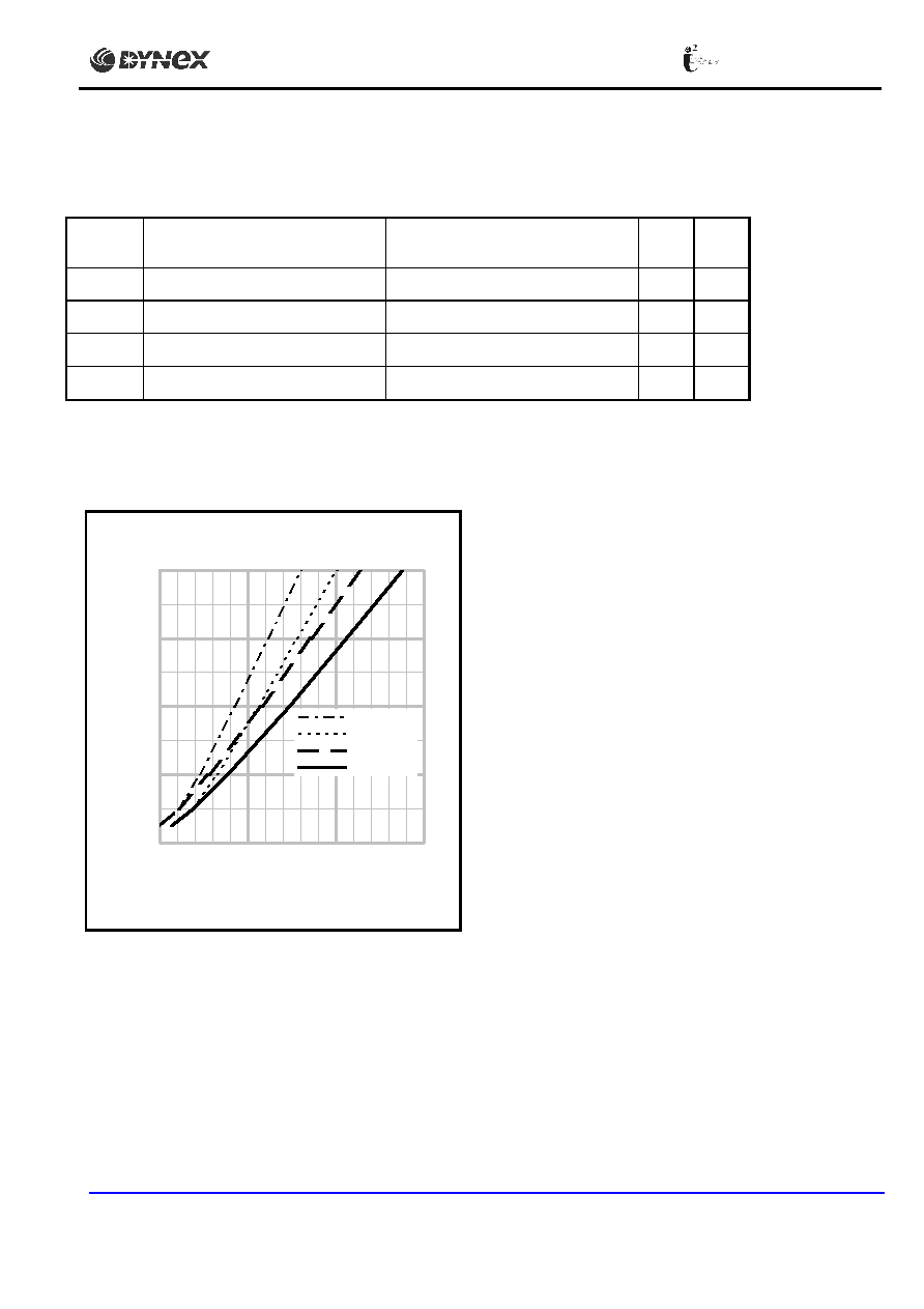
0
1
2
3
4
5
6
7
8
9
10
11
12
13
14
15
16
0
500
1000
1500
2000
Mean on-state current, I
T(AV)
- (A)
Mean power dissipation - (kW)
180
120
90
60
30
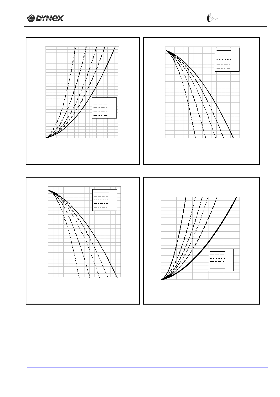
0
10
20
30
40
50
60
70
80
90
100
110
120
130
0
100 200 300 400 500 600 700 800
Mean on-state current, I
T(AV)
- (A)
Maximum case temperature, T
case
(
o
C )
180
120
90
60
30
Fig.3 On-state power dissipation ≠ sine wave
Fig.4 Maximum permissible case temperature,
double side cooled ≠ sine wave
0
10
20
30
40
50
60
70
80
90
100
110
120
130
0
100
200
300
400
500
600
700
Mean on-state current, I
T(AV)
- (A)
Maximum heatsink temperature, T
Heatsink
- (
o
C )
180
120
90
60
30
0
1
2
3
4
5
6
7
8
9
10
11
12
0
500
1000
1500
2000
2500
Mean on-state current, I
T(AV)
- (A)
Mean power dissipation - (kW)
d.c.
180
120
90
60
30
Fig.5 Maximum permissible heatsink temperature,
double side cooled ≠ sine wave
Fig.6 On-state power dissipation ≠ rectangular wave