 | –≠–ª–µ–∫—Ç—Ä–æ–Ω–Ω—ã–π –∫–æ–º–ø–æ–Ω–µ–Ω—Ç: DG406BP | –°–∫–∞—á–∞—Ç—å:  PDF PDF  ZIP ZIP |

DG406BP25
1/19
APPLICATIONS
s
Variable speed A.C. motor drive inverters (VSD-AC).
s
Uninterruptable Power Supplies
s
High Voltage Converters.
s
Choppers.
s
Welding.
s
Induction Heating.
s
DC/DC Converters.
FEATURES
s
Double Side Cooling.
s
High Reliability In Service.
s
High Voltage Capability.
s
Fault Protection Without Fuses.
s
High Surge Current Capability.
s
Turn-off Capability Allows Reduction In Equipment
Size And Weight. Low Noise Emission Reduces Acoustic
Cladding Necessary For Environmental Requirements.
KEY PARAMETERS
I
TCM
1000A
V
DRM
2500V
I
T(AV)
400A
dV
D
/dt
1000V/
µ
s
di
T
/dt
300A/
µ
s
Outline type code: P.
See Package Details for further information.
VOLTAGE RATINGS
CURRENT RATINGS
Symbol
Parameter
Conditions
Max.
I
TCM
T
HS
= 80
o
C. Double side cooled. Half sine 50Hz.
V
D
= V
DRM
, T
j
= 125
o
C, di
GQ
/dt = 30A/
µ
s, Cs = 1.0
µ
F
RMS on-state current
A
A
A
1000
400
630
Units
Repetitive peak controllable on-state current
T
HS
= 80
o
C. Double side cooled. Half sine 50Hz.
I
T(RMS)
I
T(AV)
Mean on-state current
2500
DG406BP25
Conditions
Type Number
T
vj
= 125
o
C, I
DM
= 50mA,
I
RRM
= 50mA
Repetitive Peak Off-state Voltage
V
DRM
V
Repetitive Peak Reverse Voltage
V
RRM
V
16
DG406BP25
Gate Turn-off Thyristor
Replaces March 1998 version, DS4090-2.3
DS4090-3.0 January 2000

DG406BP25
2/19
SURGE RATINGS
Conditions
8.0
0.32 x 10
6
kA
A
2
s
Surge (non-repetitive) on-state current
I
2
t for fusing
10ms half sine. T
j
= 125
o
C
10ms half sine. T
j
=125
o
C
di
T
/dt
Critical rate of rise of on-state current
300
500
V/
µ
s
Max.
Units
Rate of rise of off-state voltage
Peak stray inductance in snubber circuit
dV
D
/dt
200
nH
1000
V/
µ
s
To 66% V
DRM
; V
RG
= -2V, T
j
= 125
o
C
I
TSM
Symbol
Parameter
I
2
t
V
D
= 2000V, I
T
= 1000A, T
j
= 125
o
C, I
FG
30A,
Rise time > 1.0
µ
s
A/
µ
s
To 66% V
DRM
; R
GK
1.5
, T
j
= 125
o
C
L
S
GATE RATINGS
Symbol
Parameter
Conditions
V
Units
Max.
16
10
Min.
-
20
-
Peak reverse gate voltage
Peak forward gate current
Average forward gate power
Peak reverse gate power
Rate of rise of reverse gate current
Minimum permissable on time
Minimum permissable off time
15
60
-
20
15
-
-
µ
s
100
70
V
RGM
This value maybe exceeded during turn-off
I
FGM
P
FG(AV)
P
RGM
di
GQ
/dt
t
ON(min)
t
OFF(min)
µ
s
A/
µ
s
kW
W
A
THERMAL RATINGS AND MECHANICAL DATA
Symbol
Parameter
Conditions
Max.
Min.
R
th(c-hs)
Contact thermal resistance
R
th(j-hs)
-
-
0.1
-
0.009
o
C/W
per contact
Cathode side cooled
Double side cooled
Units
-
0.041
o
C/W
Anode side cooled
o
C/W
0.07
Virtual junction temperature
T
OP
/T
stg
Operating junction/storage temperature range
-
Clamping force
-
125
15.0
11.0
-40
kN
o
C/W
Clamping force 12.0kN
With mounting compound
DC thermal resistance - junction to heatsink
surface
T
vj
125
o
C
o
C
-
I
T
= 1000A, V
D
= V
DRM
, T
j
= 125
o
C,
di
GQ
/dt = 30A/
µ
s, Cs = 1.0
µ
F

DG406BP25
3/19
CHARACTERISTICS
Conditions
Peak reverse current
On-state voltage
V
TM
Peak off-state current
Reverse gate cathode current
50
-
Turn-on energy
Gate trigger current
Delay time
Rise time
Fall time
Gate controlled turn-off time
Turn-off energy
Storage time
Turn-off gate charge
Total turn-off gate charge
Peak reverse gate current
-
3000
V
RGM
= 16V, No gate/cathode resistor
µ
C
I
T
= 1000A, V
DM
= 2500V
Snubber Cap Cs = 1.0
µ
F,
di
GQ
/dt = 30A/
µ
s
T
j
= 125
o
C unless stated otherwise
Symbol
Parameter
I
DM
I
RRM
V
GT
Gate trigger voltage
I
GT
I
RGM
E
ON
t
d
t
r
E
OFF
t
gs
t
gf
t
gq
Q
GQ
Q
GQT
I
GQM
Min.
Max.
Units
-
2.5
V
V
DRM
= 2500V, V
RG
= 0V
-
50
mA
At V
RRM
-
50
mA
V
D
= 24V, I
T
= 100A, T
j
= 25
o
C
-
1.0
V
V
D
= 24V, I
T
= 100A, T
j
= 25
o
C
-
1.5
A
mA
mJ
1040
-
V
D
= 2000V
I
T
= 1000A, dI
T
/dt = 300A/
µ
s
I
FG
= 30A, rise time
1.0
µ
s
µ
s
1.5
-
-
3.0
µ
s
-
2300
mJ
-
14.0
µ
s
µ
s
1.5
-
µ
s
15.5
-
-
6000
µ
C
-
420
A
At 1000A peak, I
G(ON)
= 4A d.c.
DG406BP25
4/19
CURVES
-50
-25
0
25
50
75
100
125
150
Junction temperature T
j
- (∞C)
0
1.0
2.0
3.0
4.0
Gate trigger current I
GT
- (A)
0
0.5
1.0
1.5
2.0
Gate trigger voltage V
GT
- (V)
I
GT
V
GT
1.0
2.0
3.0
4.0
5.0
Instantaneous on-state voltage V
TM
- (V)
0
1.0
2.0
3.0
4.0
Instantaneous on-state current I
TM
- (kA)
Measured under pulse conditions.
I
G(ON)
= 4.0A
Half sine wave 10ms
T
j
= 125∞C
T
j
= 25∞C
0.25
0.50
1.00
1.5
2.0
Snubber capacitance C
S
- (µF)
0
0.5
1.0
1.5
Maximum permissible turn-off current I
TCM
- (kA)
Conditions:
T
j
= 125∞C, V
DM
= V
DRM
,
dI
GQ
/dt = 30A/µs
0.75
1.25
1.75
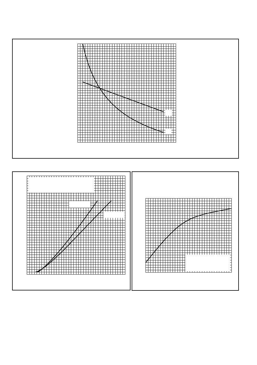
Fig.1 Maximum gate trigger voltage/current vs junction temperature
Fig.2 On-state characteristics
Fig.3 Maximum dependence of I
TCM
on C
S

DG406BP25
5/19
0
0.01
0.02
0.03
0.04
0.001
0.01
0.1
1.0
10
Time - (s)
Thermal impedance -
∞
C/W
dc
100
0.05
0
5
10
15
20
0.0001
0.001
0.01
0.1
1.0
Pulse duration - (s)
Peak half sine wave on-state current - (kA)
Fig.4 Maximum (limit) transient thermal impedance - double side cooled
Fig.5 Surge (non-repetitive) on-state current vs time