 | –≠–ª–µ–∫—Ç—Ä–æ–Ω–Ω—ã–π –∫–æ–º–ø–æ–Ω–µ–Ω—Ç: DS2107SV | –°–∫–∞—á–∞—Ç—å:  PDF PDF  ZIP ZIP |
1/8
www.dynexsemi.com
DS2107SYDS2107SV
KEY PARAMETERS
V
RRM
4500V
I
F(AV)
3329A
I
FSM
52500A
DS2107SY/DS2107SV
Rectifier Diode
Replaces December 2001 version, DS4173-4.1
DS4173-5.0 Febraury 2003
4500
4400
4300
4200
4100
4000
DS2107SY45
DS2107SY44
DS2107SY43
DS2107SY42
DS2107SY41
DS2107SY40
Conditions
V
RSM
= V
RRM
+ 100V
Lower voltage grades available.
Type Number
Repetitive Peak
Reverse Voltage
V
RRM
V
FEATURES
I Double Side Cooling
I High Surge Capability
APPLICATIONS
I Rectification
I Freewheel Diode
I DC Motor Control
I Power Supplies
I Welding
I Battery Chargers
VOLTAGE RATINGS
ORDERING INFORMATION
When ordering, select the required part number shown in the
Voltage Ratings selection table, e.g.:
DS2107SY43 for a
43
00V device in a Y outline
or
DS2107SY43 for a
43
00V device in a V outline
Note: Please use the complete part number when ordering
and quote this number in any future correspondance relating
to your order.
See Package Details for further information.
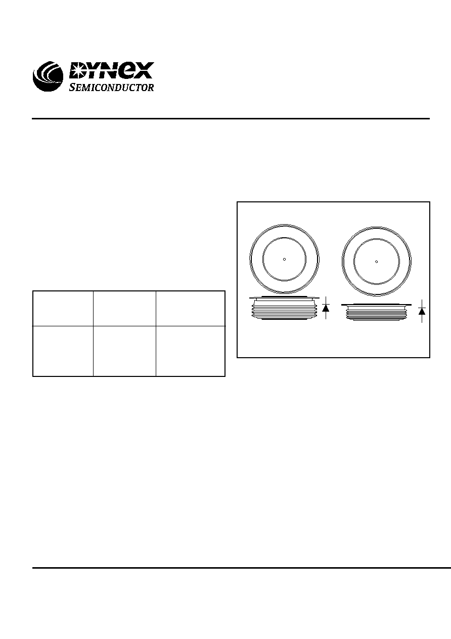
Fig. 1 Package outlines
Outline type code: Y
Outline type code: V
2/8
www.dynexsemi.com
DS2107SY/DS2107SV
Symbol
Parameter
Conditions
Double Side Cooled
I
F(AV)
Mean forward current
I
F(RMS)
RMS value
I
F
Continuous (direct) forward current
Single Side Cooled (Anode side)
I
F(AV)
Mean forward current
I
F(RMS)
RMS value
I
F
Continuous (direct) forward current
Units
Max.
Half wave resistive load
2590
A
-
4070
A
-
3510
A
Half wave resistive load
1710
A
-
2685
A
-
2110
A
CURRENT RATINGS
T
case
= 75
o
C unless otherwise stated
Symbol
Parameter
Conditions
Double Side Cooled
I
F(AV)
Mean forward current
I
F(RMS)
RMS value
I
F
Continuous (direct) forward current
Single Side Cooled (Anode side)
I
F(AV)
Mean forward current
I
F(RMS)
RMS value
I
F
Continuous (direct) forward current
Units
Max.
Half wave resistive load
3329
A
-
5229
A
-
4941
A
Half wave resistive load
2221
A
-
3489
A
-
3073
A
T
case
= 100
o
C unless otherwise stated
3/8
www.dynexsemi.com
DS2107SYDS2107SV
SURGE RATINGS
Conditions
10ms half sine; T
case
= 150
o
C
V
R
= 50% V
RRM
- 1/4 sine
10ms half sine; T
case
= 150
o
C
V
R
= 0
Max.
Units
Symbol
Parameter
I
FSM
Surge (non-repetitive) forward current
I
2
t
I
2
t for fusing
I
FSM
Surge (non-repetitive) forward current
I
2
t
I
2
t for fusing
A
2
s
52.5
kA
8.82 x 10
6
A
2
s
42.0
kA
THERMAL AND MECHANICAL DATA
dc
Conditions
Min.
Max.
Units
o
C/W
-
0.019
Anode dc
Clamping force 43.0kN
with mounting compound
Thermal resistance - case to heatsink
R
th(c-h)
0.002
Double side
-
150
o
C
T
vj
Virtual junction temperature
T
stg
Storage temperature range
Reverse (blocking)
Single side
-
Thermal resistance - junction to case
R
th(j-c)
Single side cooled
Symbol
Parameter
Clamping force
38.0
47.0
kN
≠55
150
o
C
Forward (conducting)
160
o
C
-
0.004
o
C/W
o
C/W
Cathode dc
-
0.019
o
C/W
Double side cooled
-
0.0095
o
C/W
13.8 x 10
6
-
-
4/8
www.dynexsemi.com
DS2107SY/DS2107SV
CHARACTERISTICS
Forward voltage
Peak reverse current
Parameter
µ
C
5000
Q
S
Total stored charge
Symbol
V
FM
I
RM
I
rr
Peak reverse recovery current
-
150
A
-
At V
RRM
, T
case
= 150
o
C
-
250
mA
-
1.275
V
At 3000A peak, T
case
= 25
o
C
Conditions
Min.
Max.
Units
At T
vj
= 150∞C
-
V
TO
Threshold voltage
r
T
Slope resistance
0.167
m
At T
vj
= 150∞C
-
0.77
V
I
F
= 2000A, dI
RR
/dt = 3A/
µ
s
T
case
= 150∞C, V
R
= 100V
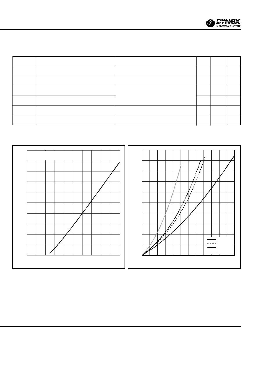
CURVES
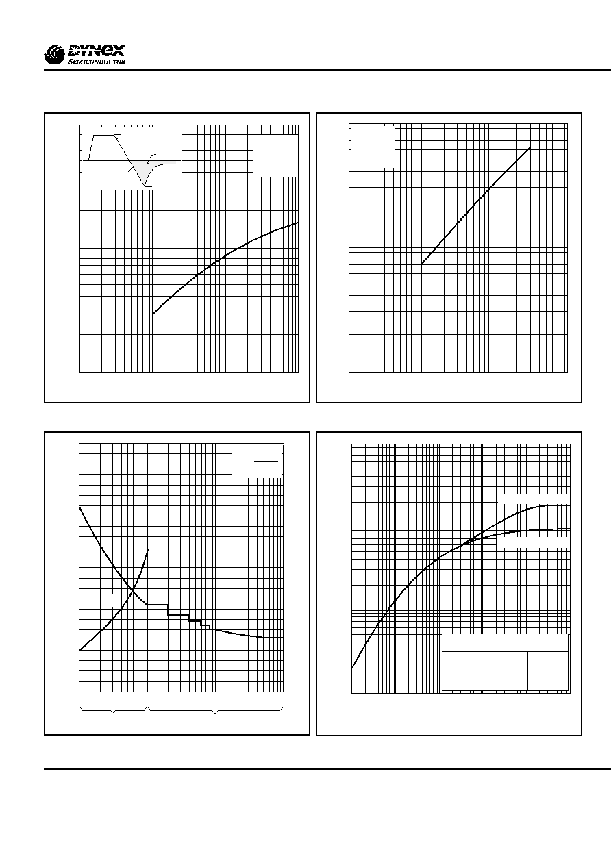
Fig.2 Maximum (limit) forward characteristics
Fig.3 Dissipation curves
V
FM
Equation:-
V
FM
= A + Bln (I
F
) + C.I
F
+D.
I
F
Where
A = 0.671711
B = 0.011006
C = 0.000158
D = 0.000604
these values are valid for T
j
= 1
50
∞C for I
F
500A to 5000A
0.5
0.7
0.9
1.1
1.5
1.3
1.4
0.6
0.8
1.0
1.2
Instantaneous forward voltage, V
F
-(V)
0
1000
2000
3000
4000
5000
Instantaneous forward current, I
F
- (A)
Measured under pulse conditions
T
j
= 150∞C
0
2000
4000
6000
Mean forward current, I
F(AV)
- (A)
0
2000
4000
6000
8000
10000
Mean power dissipation - (W)
dc
Half wave
3 phase
6 phase
5/8
www.dynexsemi.com
DS2107SYDS2107SV
Fig.4 Total stored charge
Fig.5 Maximum reverse recovery current
Fig.7 Maximum (limit) transient thermal impedance -
junction to case
Fig.6 Surge (non-repetitive) forward current vs time
(with 50% V
RRM
at T
case
150∞C)
0.1
1.0
10
100
Rate of decay of forward current, dI
F
/dt - (A/µs)
100000
10000
1000
Stored charge, Q
S
- (µ
C)
Conditions:
T
j
= 150∞C
V
R
= 100V
I
F
= 2000A
I
RR
I
F
dI
F
/dt
Q
S
0.1
1.0
10
100
Rate of decay of forward current, dI
F
/dt - (A/µs)
1000
100
10
Reverse recovery current, I
rr
- (A)
Conditions:
T
j
= 150∞C
V
R
= 100V
I
F
= 2000A
1
10
1
2
3
5
10
20
50
0
20
40
60
80
100
120
4
6
2
8
10
I
2
t value - (A
2
s x 10
6
)
ms
Cycles at 50Hz
Duration
Peak half sine forward current - (kA)
I
2
t = Œ
2
x t
2
I
2
t
10
1
0.1
0.01
0.001
Time - (s)
0.1
0.01
0.001
0.0001
Thermal impedance - (
∞
C/W)
Double side cooled
Anode side cooled
100
Conduction
d.c.
Halfwave
3 phase 120∞
6 phase 60∞
Effective thermal resistance
Junction to case ∞C/W
Double side
0.0095
0.0105
0.0112
0.0139
Single side
0.019
0.020
0.0207
0.0234