 | –≠–ª–µ–∫—Ç—Ä–æ–Ω–Ω—ã–π –∫–æ–º–ø–æ–Ω–µ–Ω—Ç: LBMM | –°–∫–∞—á–∞—Ç—å:  PDF PDF  ZIP ZIP |
LT1991
1
1991fb
, LTC and LT are registered trademarks of Linear Technology Corporation.
All other trademarks are the property of their respective owners. Patent Pending.
Precision, 100µA
Gain Selectable Amplifier
TYPICAL APPLICATIO
U
FEATURES
DESCRIPTIO
U
APPLICATIO S
U
Pin Configurable as a Difference Amplifier,
Inverting and Noninverting Amplifier
Difference Amplifier
Gain Range 1 to 13
CMRR >75dB
Noninverting Amplifier
Gain Range 0.07 to 14
Inverting Amplifier
Gain Range ≠0.08 to ≠13
Gain Error <0.04%
Gain Drift < 3ppm/∞C
Wide Supply Range: Single 2.7V to Split ±18V
Micropower: 100µA Supply Current
Precision: 50µV Maximum Input Offset Voltage
560kHz Gain Bandwidth Product
Rail-to-Rail Output
Space Saving 10-Lead MSOP and DFN Packages
Handheld Instrumentation
Medical Instrumentation
Strain Gauge Amplifiers
Differential to Single-Ended Conversion
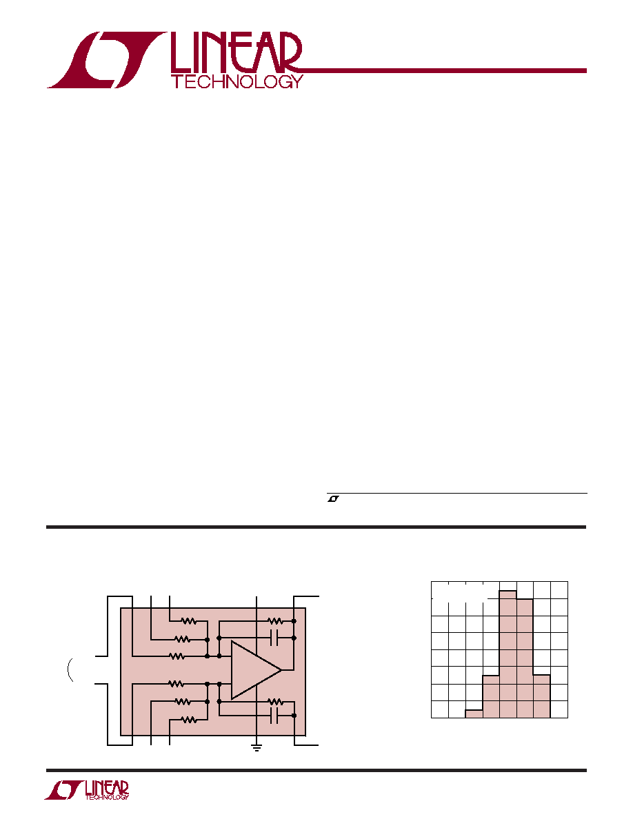
The LT
Æ
1991 combines a precision operational amplifier
with eight precision resistors to form a one-chip solution
for accurately amplifying voltages. Gains from ≠13 to 14
with a gain accuracy of 0.04% can be achieved using no
external components. The device is particularly well suited
for use as a difference amplifier, where the excellent
resistor matching results in a common mode rejection
ratio of greater than 75dB.
The amplifier features a 50µV maximum input offset
voltage and a gain bandwidth product of 560kHz. The
device operates from any supply voltage from 2.7V to 36V
and draws only 100µA supply current on a 5V supply. The
output swings to within 40mV of either supply rail.
The resistors have excellent matching, 0.04% over tem-
perature for the 450k resistors. The matching temperature
coefficent is guaranteed less than 3ppm/∞C. The resistors
are extremely linear with voltage, resulting in a gain
nonlinearity of less than 10ppm.
The LT1991 is fully specified at 5V and ±15V supplies and
from ≠40∞C to 85∞C. The device is available in space
saving 10-lead MSOP and low profile (0.8mm) 3mm ◊
3mm DFN packages.
Rail-to-Rail Gain = 1 Difference Amplifier
Distribution of Resistor Matching
≠
+
5V
V
IN
V
M(IN)
V
P(IN)
≠
+
V
OUT
= V
REF
+
V
IN
SWING 40mV TO
EITHER RAIL
R
OUT
<0.1
V
REF
=
2.5V
INPUT RANGE
≠ 0.5V TO 5.1V
R
IN
= 900k
LT1991
1991 TA01
50k
50k
150k
150k
450k
450k
4pF
450k
450k
4pF
RESISTOR MATCHING (%)
PERCENTAGE OF UNITS (%)
0.04
1991TA01b
≠ 0.02
0
0.02
40
35
30
25
20
15
10
5
0
≠ 0.04
450k RESISTORS
LT1991A

LT1991
2
1991fb
SYMBOL
PARAMETER
CONDITIONS
MIN
TYP
MAX
UNITS
G
Gain Error
V
S
= ±15V, V
OUT
= ±10V; R
L
= 10k
G = 1; LT1991A
±0.04
%
G = 1; LT1991
±0.08
%
G = 3 or 9; LT1991A
±0.06
%
G = 3 or 9; LT1991
±0.12
%
GNL
Gain Nonlinearity
V
S
= ±15V; V
OUT
= ±10V; R
L
= 10k
1
10
ppm
G/T
Gain Drift vs Temperature (Note 6)
V
S
= ±15V; V
OUT
= ±10V; R
L
= 10k
0.3
3
ppm/∞C
CMRR
Common Mode Rejection Ratio,
V
S
= ±15V; V
CM
= ±15.2V
Referred to Inputs (RTI)
G = 9; LT1991A
80
100
dB
G = 3; LT1991A
75
93
dB
G = 1; LT1991A
75
90
dB
Any Gain; LT1991
60
70
dB
V
CM
Input Voltage Range (Note 7)
P1/M1 Inputs
V
S
= ±15V; V
REF
= 0V
≠28
27.6
V
V
S
= 5V, 0V; V
REF
= 2.5V
≠0.5
5.1
V
V
S
= 3V, 0V; V
REF
= 1.25V
0.75
2.35
V
ABSOLUTE AXI U
RATI GS
W
W
W
U
(Note 1)
ELECTRICAL CHARACTERISTICS
The
denotes the specifications which apply over the full operating
temperature range, otherwise specifications are at T
A
= 25∞C. Difference amplifier configuration, V
S
= 5V, 0V or ±15V;
V
CM
= V
REF
= half supply, unless otherwise noted.
Total Supply Voltage (V
+
to V
≠
) ............................... 40V
Input Voltage (Pins P1/M1, Note 2) ....................... ±60V
Input Voltage
(Other inputs Note 2).............. V
+
+ 0.2V to V
≠
≠ 0.2V
Output Short-Circuit Duration (Note 3) ............ Indefinite
Operating Temperature Range (Note 4) ...≠40∞C to 85∞C
Specified Temperature Range (Note 5) ....≠40∞C to 85∞C
ORDER PART
NUMBER
DD PART MARKING*
T
JMAX
= 150∞C,
JA
= 230∞C/W
LBMM
LT1991CDD
LT1991IDD
LT1991ACDD
LT1991AIDD
*Temperature and electrical grades are identified by a label on the shipping container. Consult LTC Marketing for parts specified with wider operating temperature ranges.
Maximum Junction Temperature
DD Package ...................................................... 125∞C
MS Package ..................................................... 150∞C
Storage Temperature Range
DD Package .......................................≠65∞C to 125∞C
MS Package ......................................≠65∞C to 150∞C
Lead Temperature (Soldering, 10 sec).................. 300∞C
ORDER PART
NUMBER
MS PART MARKING*
LTQD
LT1991CMS
LT1991IMS
LT1991ACMS
LT1991AIMS
EXPOSED PAD CONNECTED TO V
EE
PCB
CONNECTION OPTIONAL
T
JMAX
= 125∞C,
JA
= 160∞C/W
PACKAGE/ORDER I FOR ATIO
U
U
W
TOP VIEW
DD PACKAGE
10-LEAD (3mm ◊ 3mm) PLASTIC DFN
10
9
6
7
8
4
5
3
2
1
M1
M3
M9
V
CC
OUT
P1
P3
P9
V
EE
REF
1
2
3
4
5
P1
P3
P9
V
EE
REF
10
9
8
7
6
M1
M3
M9
V
CC
OUT
TOP VIEW
MS PACKAGE
10-LEAD PLASTIC MSOP
LT1991
3
1991fb
SYMBOL
PARAMETER
CONDITIONS
MIN
TYP
MAX
UNITS
V
CM
Input Voltage Range (Note 7)
P1/M1 Inputs, P9/M9 Connected to REF
V
S
= ±15V; V
REF
= 0V
≠60
60
V
V
S
= 5V, 0V; V
REF
= 2.5V
≠14
16.8
V
V
S
= 3V, 0V; V
REF
= 1.25V
≠1.5
7.3
V
P3/M3 Inputs
V
S
= ±15V; V
REF
= 0V
≠15.2
15.2
V
V
S
= 5V, 0V; V
REF
= 2.5V
0.5
4.2
V
V
S
= 3V, 0V; V
REF
= 1.25V
0.95
1.95
V
P9/M9 Inputs
V
S
= ±15V; V
REF
= 0V
≠15.2
15.2
V
V
S
= 5V, 0V; V
REF
= 2.5V
0.85
3.9
V
V
S
= 3V, 0V; V
REF
= 1.25V
1.0
1.9
V
V
OS
Op Amp Offset Voltage (Note 8)
LT1991AMS, V
S
= 5V, 0V
15
50
µV
135
µV
LT1991AMS, V
S
= ±15V
15
80
µV
160
µV
LT1991MS
25
100
µV
200
µV
LT1991DD
25
150
µV
250
µV
V
OS
/T
Op Amp Offset Voltage Drift (Note 6)
0.3
1
µV/∞C
I
B
Op Amp Input Bias Current
2.5
5
nA
7.5
nA
I
OS
Op Amp Input Offset Current
LT1991A
50
500
pA
750
pA
LT1991
50
1000
pA
1500
pA
Op Amp Input Noise Voltage
0.01Hz to 1Hz
0.35
µV
P-P
0.01Hz to 1Hz
0.07
µV
RMS
0.1Hz to 10Hz
0.25
µV
P-P
0.1Hz to 10Hz
0.05
µV
RMS
e
n
Input Noise Voltage Density
G = 1; f = 1kHz
180
nV/Hz
G = 9; f = 1kHz
46
nV/Hz
R
IN
Input Impedance (Note 10)
P1 (M1 = Ground)
630
900
1170
k
P3 (M3 = Ground)
420
600
780
k
P9 (M9 = Ground)
350
500
650
k
M1 (P1 = Ground)
315
450
585
k
M3 (P3 = Ground)
105
150
195
k
M9 (P9 = Ground)
35
50
65
k
R
Resistor Matching
450k Resistors, LT1991A
0.01
0.04
%
(Note 9)
Other Resistors, LT1991A
0.02
0.06
%
450k Resistors, LT1991
0.02
0.08
%
Other Resistors, LT1991
0.04
0.12
%
R/T
Resistor Temperature Coefficient (Note 6)
Resistor Matching
0.3
3
ppm/∞C
Absolute Value
≠30
ppm/∞C
PSRR
Power Supply Rejection Ratio
V
S
= ±1.35V to ±18V (Note 8)
105
135
dB
Minimum Supply Voltage
2.4
2.7
V
The
denotes the specifications which apply over the full operating
temperature range, otherwise specifications are at T
A
= 25∞C. Difference amplifier configuration, V
S
= 5V, 0V or ±15V;
V
CM
= V
REF
= half supply, unless otherwise noted.
ELECTRICAL CHARACTERISTICS

LT1991
4
1991fb
The
denotes the specifications which apply over the full operating
temperature range, otherwise specifications are at T
A
= 25∞C. Difference amplifier configuration, V
S
= 5V, 0V or ±15V;
V
CM
= V
REF
= half supply, unless otherwise noted.
SYMBOL
PARAMETER
CONDITIONS
MIN
TYP
MAX
UNITS
V
OUT
Output Voltage Swing (to Either Rail)
No Load
V
S
= 5V, 0V
40
55
mV
V
S
= 5V, 0V
65
mV
V
S
= ±15V
110
mV
1mA Load
V
S
= 5V, 0V
150
225
mV
V
S
= 5V, 0V
275
mV
V
S
= ±15V
300
mV
I
SC
Output Short-Circuit Current (Sourcing)
Drive Output Positive;
8
12
mA
Short Output to Ground
4
mA
Output Short-Circuit Current (Sinking)
Drive Output Negative;
8
21
mA
Short Output to V
S
or Midsupply
4
mA
BW
≠3dB Bandwidth
G = 1
110
kHz
G = 3
78
kHz
G = 9
40
kHz
GBWP
Op Amp Gain Bandwidth Product
f = 10kHz
560
kHz
t
r
, t
f
Rise Time, Fall Time
G = 1; 0.1V Step; 10% to 90%
3
µs
G = 9; 0.1V Step; 10% to 90%
8
µs
t
s
Settling Time to 0.01%
G = 1; V
S
= 5V, 0V; 2V Step
42
µs
G = 1; V
S
= 5V, 0V; ≠2V Step
48
µs
G = 1; V
S
= ±15V, 10V Step
114
µs
G = 1; V
S
= ±15V, ≠10V Step
74
µs
SR
Slew Rate
V
S
= 5V, 0V; V
OUT
= 1V to 4V
0.06
0.12
V/µs
V
S
= ±15V; V
OUT
= ±10V
0.08
0.12
V/µs
I
S
Supply Current
V
S
= 5V, 0V
100
110
µA
150
µA
V
S
= ±15V
130
160
µA
210
µA
Note 1: Absolute Maximum Ratings are those beyond which the life of the
device may be impaired.
Note 2: The P3/M3 and P9/M9 inputs should not be taken more than 0.2V
beyond the supply rails. The P1/M1 inputs can withstand ±60V if P9/M9
are grounded and V
S
= ±15V (see Applications Information section about
"High Voltage CM Difference Amplifiers").
Note 3: A heat sink may be required to keep the junction temperature
below absolute maximum ratings.
Note 4: Both the LT1991C and LT1991I are guaranteed functional over the
≠40∞C to 85∞C temperature range.
Note 5: The LT1991C is guaranteed to meet the specified performance
from 0∞C to 70∞C and is designed, characterized and expected to meet
specified performance from ≠40∞C to 85∞C but is not tested or QA
sampled at these temperatures. The LT1991I is guaranteed to meet
specified performance from ≠40∞C to 85∞C.
Note 6: This parameter is not 100% tested.
Note 7: Input voltage range is guaranteed by the CMRR test at V
S
= ±15V.
For the other voltages, this parameter is guaranteed by design and through
correlation with the ±15V test. See the Applications Information section to
determine the valid input voltage range under various operating
conditions.
Note 8: Offset voltage, offset voltage drift and PSRR are defined as
referred to the internal op amp. You can calculate output offset as follows.
In the case of balanced source resistance, V
OS,OUT
= V
OS
∑ NOISEGAIN +
I
OS
∑ 450k + I
B
∑ 450k ∑ (1≠ R
P
/R
N
) where R
P
and R
N
are the total
resistance at the op amp positive and negative terminal respectively.
Note 9: Applies to resistors that are connected to the inverting inputs.
Resistor matching is not tested directly, but is guaranteed by the gain
error test.
Note 10: Input impedence is tested by a combination of direct
measurements and correlation to the CMRR and gain error tests.
ELECTRICAL CHARACTERISTICS

LT1991
5
1991fb
Output Voltage Swing vs Load
Current (Output High)
Output Short-Circuit Current vs
Temperature
Input Offset Voltage vs
Difference Gain
Output Offset Voltage vs
Difference Gain
Gain Error vs Load Current
Slew Rate vs Temperature
(Difference Amplifier Configuration)
Supply Current vs Supply Voltage
Output Voltage Swing vs
Temperature
Output Voltage Swing vs Load
Current (Output Low)
TYPICAL PERFOR A CE CHARACTERISTICS
U
W
SUPPLY VOLTAGE (±V)
0
SUPPLY CURRENT (
µ
A)
200
175
150
125
100
75
50
25
0
16
1991 G01
4
2
6
10
14
18
8
12
20
T
A
= 85∞C
T
A
= ≠40∞C
T
A
= 25∞C
TEMPERATURE (∞C)
≠50
OUTPUT VOLTAGE SWING (mV)
100
1991 G02
0
50
60
40
20
V
EE
≠25
25
75
125
V
S
= 5V, 0V
NO LOAD
OUTPUT HIGH
(RIGHT AXIS)
OUTPUT LOW
(LEFT AXIS)
V
CC
≠20
≠40
≠60
LOAD CURRENT (mA)
0
OUTPUT VOLTAGE (mV)
1400
1200
1000
800
600
400
200
V
EE
1991 G03
2
10
9
8
7
6
5
1
3
4
V
S
= 5V, 0V
T
A
= 85∞C
T
A
= ≠40∞C
T
A
= 25∞C
LOAD CURRENT (mA)
V
CC
≠100
≠200
≠300
≠400
≠500
≠600
≠700
≠800
≠900
≠1000
OUTPUT VOLTAGE SWING (mV)
1991 G04
0
1
2
3
4
5
6
7
8
9
10
V
S
= 5V, 0V
T
A
= 85∞C
T
A
= ≠40∞C
T
A
= 25∞C
TEMPERATURE (∞C)
≠50
OUTPUT SHORT-CIRCUIT CURRENT (mA)
25
20
15
10
5
0
0
50
75
1991 G05
≠25
25
100
125
V
S
= 5V, 0V
SINKING
SOURCING
GAIN (V/V)
1
INPUT OFFSET VOLTAGE (
µ
V)
150
100
50
0
≠50
≠100
≠150
12
9 10 11
13
5
1991 G06
2
3
8
7
6
4
V
S
= 5V, 0V
REPRESENTATIVE PARTS
GAIN (V/V)
1
OUTPUT OFFSET VOLTAGE (
µ
V)
1000
750
500
250
0
≠250
≠500
≠750
≠1000
12
9 10 11
13
5
1991 G07
2
3
8
7
6
4
V
S
= 5V, 0V
REPRESENTATIVE PARTS
LOAD CURRENT (mA)
0
GAIN ERROR (%)
3
5
1991 G08
1
2
4
0.04
0.03
0.02
0.01
0
≠0.01
≠0.02
≠0.03
≠0.04
GAIN = 1
V
S
= ±15V
V
OUT
= ±10V
T
A
= 25∞C
REPRESENTATIVE UNITS
TEMPERATURE (∞C)
≠50
SLEW RATE (V/
µ
s)
0.30
0.25
0.20
0.15
0.10
0.05
0
25
75
1991 G09
≠25
0
50
100
125
GAIN = 1
V
S
= ±15V
V
OUT
= ±10V
SR
≠
(FALLING EDGE)
SR
+
(RISING EDGE)