Linear Integrated Systems
Linear Integrated Systems
310 S. Milpitas Blvd., Milpitas, CA 95035 TEL: (408) 263-8401 ∑ FAX: (408) 263-7280
FEATURES
VERY HIGH INPUT IMPEDANCE
HIGH GATE BREAKDOWN
ULTRA LOW LEAKAGE
LOW CAPACITANCE
MONOLITHIC DUAL
ABSOLUTE MAXIMUM RATINGS (NOTE 1)
(T
A
= 25
∞
C unless otherwise noted)
Drain-Source or Drain-Gate Voltage
-40V (NOTE 2)
Transient G-S Voltages (NOTES 2 and 3)
±
125V
Gate-Gate Voltage
±
80V
Drain Current (NOTE 2)
50mA
Storage Temperature
-65
∞
C to +200
∞
C
Power Dissipation
375 mW
MONOLITHIC DUAL
P-CHANNEL ENHANCEMENT MODE
MOSFET
3N190, 3N191
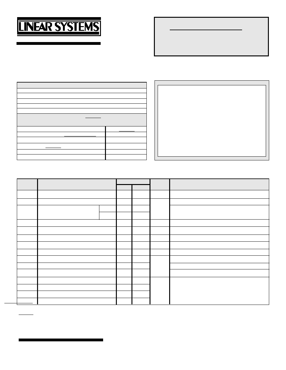
TO-99
Bottom View
DIE MAP
ELECTRICAL CHARACTERISTICS @ 25
∞
C (unless otherwise specified)
LIMITS
SYMBOL CHARACTERISTICS
MIN.
MAX.
UNITS
CONDITIONS
I
GSSF
Gate Forward Leakage Current
--
10
pA
V
GS
= 40 V
I
GSSR
Gate Reverse Leakage Current
--
-10
pA
V
GS
= -40 V
I
DSS
Drain to Source Leakage Current
--
-200
V
DS
= -15 V
I
SDS
Source-Drain Current
--
-400
V
SD
= -20V
V
DB
= 0
I
D(on)
ON Drain Current
-5
-30
mA
V
DS
= -15 V
V
GS
= -10 V
r
DS(on)
Drain-Source ON Resistance
--
300
ohms
V
DS
= -20 V
I
D
= -100
µ
A
V
DS(on)
Drain-Source ON Voltage
--
2.0
V
V
GS
= -10 V
I
D
= 10 mA
g
fs
Forward Transconductance
1500
4000
µ
s
V
DS
= -15V
I
D
= 10mA
g
os
Output Admittance
--
300
f=1KHz
C
iss
Input Capacitance
--
4.5
pF
f=1MHz
C
rss
Reverse Transfer Capacitance
--
1.0
C
oss
Output Capacitance Input Shorted
--
3.0
MATCHING CHARACTERISTICS 3N190
Y
fs1
/
Y
fs2
Forward Transconductance Ratio
0.85
1.0
V
DS
= -15V
I
D
= -500
µ
A
f=1KHz
V
GS1-2
Offset Voltage
--
100
mV
V
DS
= -15V
I
D
= -500
µ
A
V
GS1-2
Drift vs. Temperature
--
100
µ
V/
∞
C
V
DS
= -15V
I
D
= -500
µ
A
T
A
= -55
∞
C to +125
∞
C
NOTES: 1. These ratings are limiting values above which the serviceability of the semiconductor may be impaired.
2. Per Transistor.
3. Approximately doubles for every 10
∞
C increase in T
A
.
T

Linear Integrated Systems
310 S. Milpitas Blvd., Milpitas, CA 95035 TEL: (408) 263-8401 ∑ FAX: (408) 263-7280
LIMITS
SYMBOL CHARACTERISTICS
MIN. MAX. UNITS CONDITIONS
Y
fs1
/Y
fs2
Forward Transconductance Ratio
0.90
1.0
V
DS
= -15 V
I
D
= -500
µ
A
f=1kHz
V
GS1-2
Gate Source Threshold Voltage Differential
--
100
mV
V
DS
= -15 V
I
D
= -500
µ
A
V
GS1-2
/
T
Gate Source Threshold Voltage Differential
--
100
µ
V/
∞
C
V
DS
= -15 V
I
A
= -500
µ
A
Change with Temperature
T
A
= -55
∞
C to = +25
∞
C
MATCHING CHARACTERISTICS 3N165
90%
Switching Times Test Circuit
V
DD
1
2
OUT
V
R
R
50
Switching Times Test Circuit
t
10%
10%
10%
10%
t
on
r
off
t
INPUT PULSE
Rise Time 2ns
Pulse Width 200ns
SAMPLING SCOPE
T 0.2ns
C 2pF
R 10M
r
IN
IN
TYPICAL SWITCHING WAVEFORM
NOTES:
1. MOS field-effect transistors have extremely high input resistance and can be damaged by the accumulation of excess static
charge. To avoid possible damage to the device while wiring, testing, or in actual operation, follow these procedures:
To avoid the build-up of static charge, the leads of the devices should remain shorted together with a metal ring except when
being tested or used. Avoid unnecessary handling. Pick up devices by the case instead of the leads. Do not insert or remove
devices from circuits with the power on, as transient voltages may cause permanant damage to the devices.
2. Per transistor.
3. Devices must mot be tested at
±
125V more than once, nor for longer than 300ms.
4. For design reference only, not 100% tested.
Stresses above those listed under "Absolute Maximum Ratings" may cause permanent damage to the device. These are stress
ratings only and functional operation of the device at these or any other conditions above those indicated in the operational
sections of the specifications is not implied. Exposure to absolute maximum rating conditions for extended periods may affect
device reliability.