Linear Integrated Systems
Linear Integrated Systems
4042 Clipper Court, Fremont, CA 94538 ∑ TEL: (510) 490-9160 ∑ FAX: (510) 353-0261
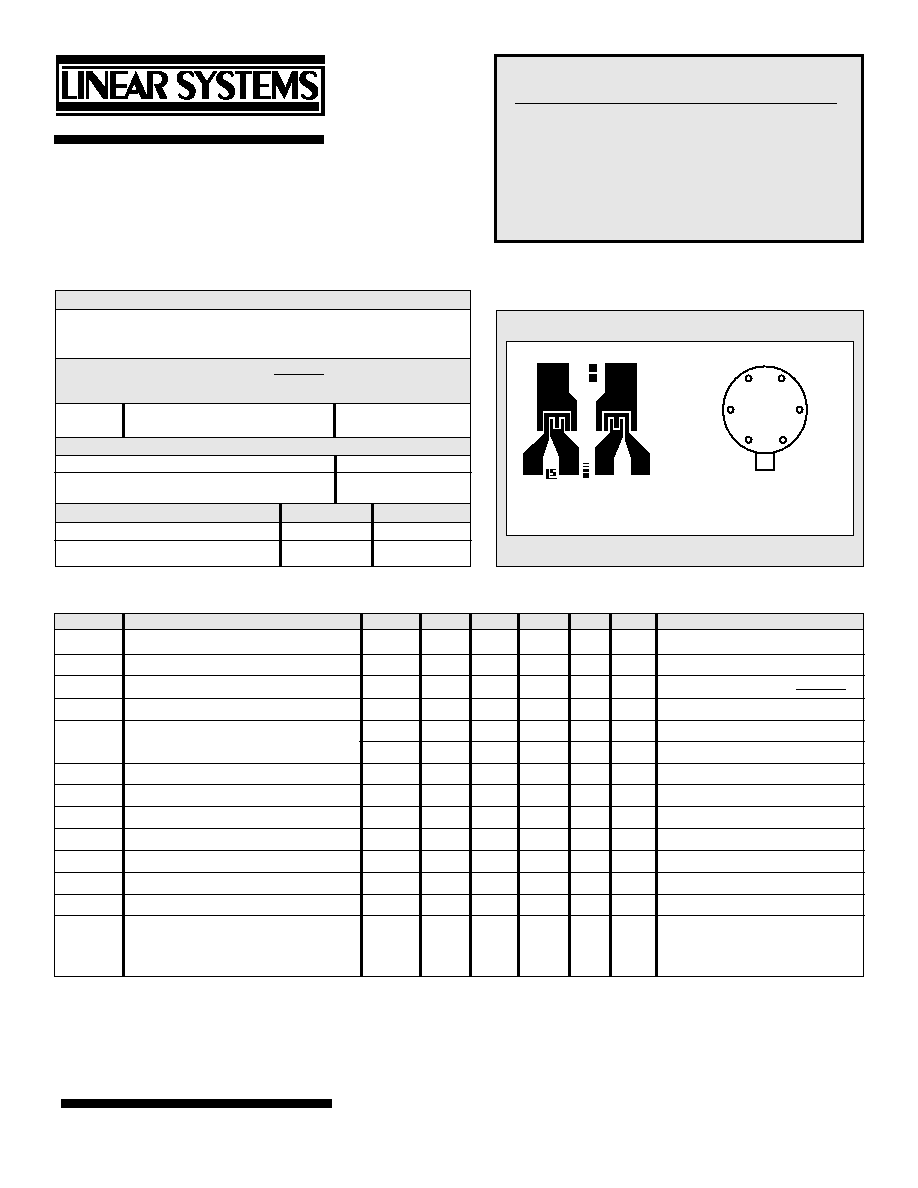
1 7
3
5
BOTTOM VIEW
2
6
B1 E1 E2 B2
C1
C2
26 X 29 MILS
E1
E2
C1
C2
B1
B2
MONOLITHIC DUAL
PNP
TRANSISTORS
IT130A IT130 IT131 IT132
FEATURES
Direct Replacement for Intersil IT130 Series
Pin for Pin Compatible
ABSOLUTE MAXIMUM RATINGS NOTE 1
(T
A
= 25
∞
C unless otherwise noted)
I
C
Collector Current
10mA
Maximum Temperatures
Storage Temperature Range
-65
∞
C to +200
∞
C
Operating Junction Temperature
+150
∞
C
Maximum Power Dissipation ONE SIDE BOTH SIDES
Device Dissipation @ Free Air
250mW
500mW
Linear Derating Factor
2.3mW/
∞
C
4.3mW/
∞
C
SYMBOL CHARACTERISTICS IT130A IT130 IT131 IT132 UNITS CONDITIONS
BV
CBO
Collector to Base Voltage
45
45
45
45
MIN.
V
I
C
= 10
µ
A
I
E
= 0
BV
CEO
Collector to Emitter Voltage
45
45
45
45
MIN.
V
I
C
= 10
µ
A
I
B
= 0
BV
EBO
Emitter-Base Breakdown Voltage
6.2
6.2
6.2
6.2
MIN.
V
I
E
= 10
µ
A
I
C
= 0
NOTE 2
BV
CCO
Collector to Collector Voltage
60
60
60
60
MIN.
V
I
C
= 10
µ
A
I
E
= 0
h
FE
DC Current Gain
200
200
80
80
MIN.
I
C
= 10
µ
A
V
CE
= 5V
225
225
100
100
MIN.
I
C
= 1.0mA V
CE
= 5V
V
CE
(SAT) Collector Saturation Voltage
0.5
0.5
0.5
0.5
MAX.
V
I
C
= 0.5mA I
B
= 0.05mA
I
EBO
Emitter Cutoff Current
1
1
1
1
MAX.
nA
I
C
= 0
V
EB
= 3V
I
CBO
Collector Cutoff Current
1
1
1
1
MAX.
nA
I
E
= 0
V
CB
= 45V
C
OBO
Output Capacitance
2
2
2
2
MAX.
pF
I
E
= 0
V
CB
= 5V
C
C1C2
Collector to Collector Capacitance
4
4
4
4
MAX.
pF
V
CC
= 0
I
C1C2
Collector to Collector Leakage Current
10
10
10
10
MAX.
nA
V
CC
=
±
60V
f
T
Current Gain Bandwidth Product
110
110
90
90
MIN.
MHz
I
C
= 1mA
V
CE
= 5V
NF
Narrow Band Noise Figure
3
3
3
3
MAX.
dB
I
C
= 100
µ
A V
CE
= 5V
BW = 200Hz, R
G
= 10 K
f=1KHz
ELECTRICAL CHARACTERISTICS T
A
= 25
∞
C (unless otherwise noted)
Linear Integrated Systems
4042 Clipper Court, Fremont, CA 94538 ∑ TEL: (510) 490-9160 ∑ FAX: (510) 353-0261
MATCHING CHARACTERISTICS @ 25
∞
C (unless otherwise noted)
SYMBOL
CHARACTERISTICS
IT130A IT130 IT131 IT132 UNITS CONDITIONS
|V
BE1
-V
BE2
|
Base Emitter Voltage Differential
1
2
3
5
MAX. mV
I
C
= 10
µ
A
V
CE
= 5V
|(V
BE1
-V
BE2
)|/
T Base Emitter Voltage Differential
3
5
10
20
MAX.
µ
V/
∞
C
I
C
= 10
µ
A
V
CE
= 5V
Change with Temperature
T = -55
∞
C to +125
∞
C
|I
B1
- I
B2
|
Base Current Differential
2.5
5
25
25
MAX. nA
I
C
= 10
µ
A
V
CE
= 5V
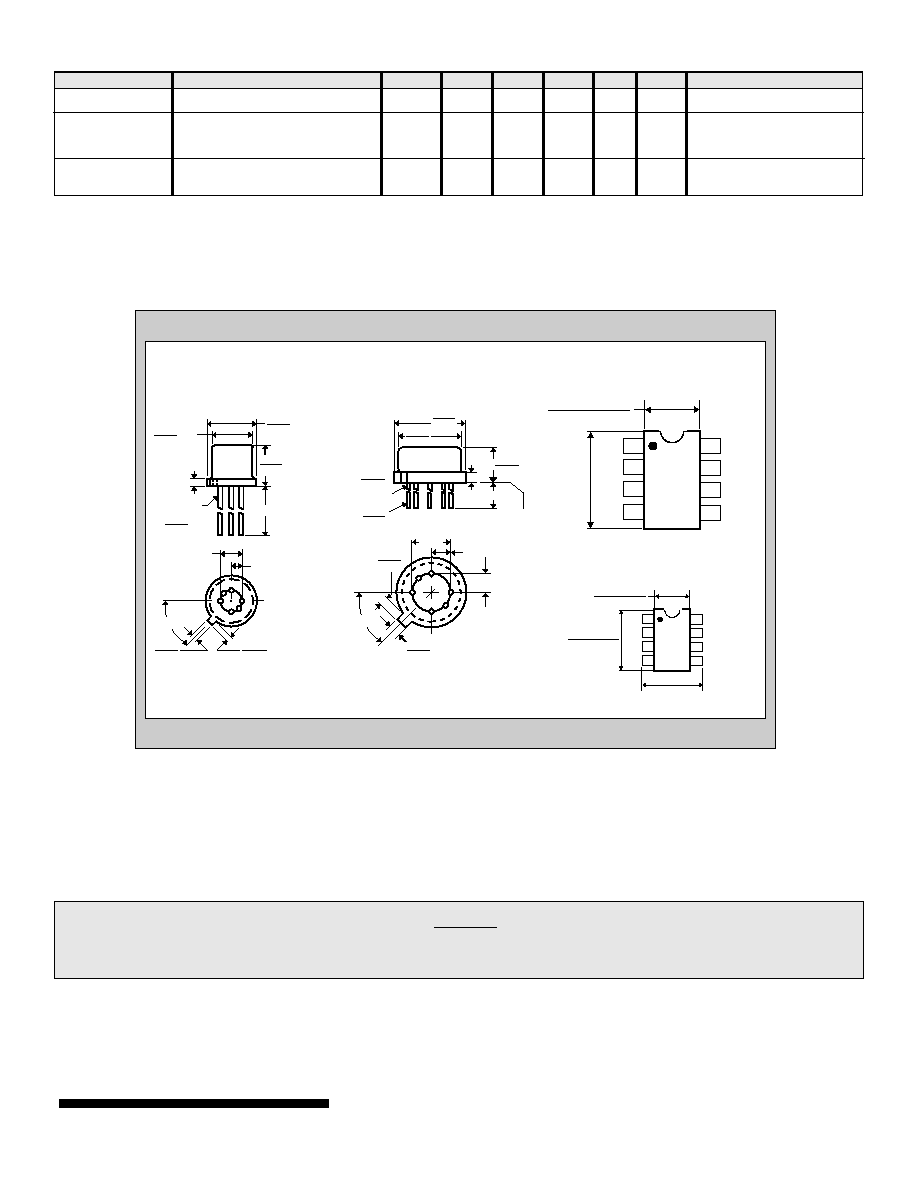
TO-71
Six Lead
0.230
0.209
DIA.
DIA.
0.195
0.175
0.030
MAX.
0.500 MIN.
0.150
0.115
0.019
0.016
DIA.
6 LEADS
3
2
1
8
4
5
6
0.046
0.036
45∞
0.048
0.028
0.100
0.050
7
TO-78
0.335
0.370
0.305
0.335
0.016
0.019
0.165
0.185
0.040
MAX.
DIM. A
0.016
0.021
DIM. B
MIN. 0.500
0.200
0.100
0.100
0.028
0.034
45∞
1
2 3 4
5
6
7
8
0.029
0.045
SEATING
PLANE
C1 1
2
3
4
5
6
7
8
B1
E1
N/C
N/C
C2
B2
E2
P-DIP
C1 1
2
3
4
5
6
7
8
B1
E1
N/C
N/C
C2
B2
E2
0.150
0.158
(3.81)
(4.01)
0.188
0.197
0.228
0.244
(5.79)
(6.20)
SOIC
N/C
0.320
0.290
(8.13)
(7.37)
0.405
MAX.
(10.29)
(4.78)
(5.00)
NOTES:
1. These ratings are limiting values above which the serviceability of any semiconductor may be impaired.
2. The reverse base-to-emitter voltage must never exceed 6.2 volts; the reverse base-to-emitter current must never exceed 10
µ
A.