 | –≠–ª–µ–∫—Ç—Ä–æ–Ω–Ω—ã–π –∫–æ–º–ø–æ–Ω–µ–Ω—Ç: LT1935ES5 | –°–∫–∞—á–∞—Ç—å:  PDF PDF  ZIP ZIP |
1
LT1935
1935f
DESCRIPTIO
U
FEATURES
APPLICATIO S
U
TYPICAL APPLICATIO
U
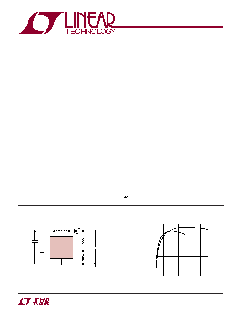
1.2MHz Boost DC/DC
Converter in ThinSOT
with 2A Switch
1.2MHz Switching Frequency
High Output Voltage: Up to 38V
Wide Input Range: 2.3V to 16V
Low V
CESAT
Switch: 180mV at 2A
Soft-Start
Uses Small Surface Mount Components
5V at 1A from 3.3V Input
12V at 600mA from 5V Input
Low Shutdown Current: < 1µA
Pin-for-Pin Compatible with the LT1613 and LT1930
Low Profile (1mm) SOT-23 (ThinSOT
TM
) Package
The LT
Æ
1935 is the industry's highest power SOT-23
switching regulator. Its unprecedented 2A, 40V internal
switch allows high output currents to be generated in a
small footprint. Intended for space-conscious applica-
tions, the LT1935 switches at 1.2MHz, allowing the use of
tiny, low profile inductors and capacitors 2mm or less in
height. The NPN switch achieves a V
CESAT
of just 180mV
at 2A independent of supply voltage, resulting in high
efficiency even at maximum power levels from a 3V input.
A constant frequency, internally compensated, current
mode PWM architecture results in low, predictable output
noise that is easy to filter. Low ESR ceramic capacitors can
be used on the output, further reducing noise to the
millivolt level. The high voltage switch on the LT1935 is
rated at 40V, making the device ideal for boost converters
up to 38V as well as for single-ended primary inductance
converter (SEPIC) and flyback designs. The device can
generate 5V at up to 1A from a 3.3V supply or 5V at 550mA
from four alkaline cells in a SEPIC design.
The LT1935 is available in a 5-lead SOT-23 package.
Figure 1. 5V to 12V, 600mA Step-Up DC/DC Converter
Digital Cameras
Battery Backup
LCD Bias
Local 5V or 12V Supply
PC Cards
xDSL Power Supply
TFT-LCD Bias Supply
, LTC and LT are registered trademarks of Linear Technology Corporation.
GND
V
IN
SW
SHDN
FB
V
IN
5V
D1
L1
4.2µH
84.5k
LT1935
1935 F01
10µF
4.7µF
10k
V
OUT
12V
600mA
D1: ON SEMI MBRM120
L1: SUMIDA CDRH5D28-4R2
ON OFF
ThinSOT is a trademark of Linear Technology Corporation.
LOAD CURRENT (mA)
0
EFFICIENCY (%)
600
1935 F01b
200
100
300
500
700
400
90
85
80
75
70
65
60
55
50
V
IN
= 5V
V
IN
= 3.3V
Efficiency, V
OUT
= 12V
2
LT1935
1935f
PARAMETER
CONDITIONS
MIN
TYP
MAX
UNITS
Feedback Voltage
Measured at the FB Pin
1.240
1.265
1.280
V
Feedback Voltage Line Regulation
2.5V V
IN
16V
0.01
%/V
FB Pin Bias Current
V
FB
= V
REF
12
60
nA
Undervoltage Lockout Threshold
2.1
2.3
V
Maximum Input Voltage
16
V
Switching Frequency
1
1.2
1.4
MHz
Maximum Duty Cycle
85
93
%
Switch Current Limit
(Note 3)
2
3.2
A
Switch Saturating Voltage
I
SW
= 2A
180
280
mV
Switch Leakage Current
V
SW
= 5V
0.01
1
µA
SHDN Pin Input Current
V
SHDN
= 1.8V
14
40
µA
V
SHDN
= 0V
0.1
µA
Operating Supply Current
V
FB
= 1.5V
3
mA
SHDN Supply Current
V
SHDN
= 0V
0.1
1
µA
SHDN Input High Voltage
1.8
V
SHDN Input Low Voltage
0.5
V
(Note 1)
V
IN
Voltage .............................................................. 16V
SW Voltage ................................................ ≠ 0.4V to 40V
FB Voltage ................................................................. 6V
Current Into FB Pin .............................................. ±1mA
SHDN Voltage ......................................................... 16V
Maximum Junction Temperature ......................... 125∞C
Operating Ambient Temperature Range
(Note 2) .............................................. ≠ 40∞C to 85∞C
Storage Temperature Range ................. ≠ 65∞C to 150∞C
Strict adherence to JDEC 020B solder attach and rework
for assemblies containing lead is recommended.
Consult LTC marketing for parts specified with wider operating temperature ranges.
The
denotes specifications which apply over the full operating temperature range, otherwise specifications are T
A
= 25∞C.
V
IN
= 3V, V
SHDN
= V
IN
unless otherwise noted. (Note 2)
ORDER PART
NUMBER
LT1935ES5
S5 PART MARKING
LTRX
T
JMAX
= 125∞C,
JA
= 113∞C/ W,
ELECTRICAL CHARACTERISTICS
PACKAGE/ORDER I FOR ATIO
U
U
W
ABSOLUTE AXI U RATI GS
W
W
W
U
Note 1: Absolute Maximum Ratings are those values beyond which the life
of a device may be impaired.
Note 2: The LT1935ES5 is guaranteed to meet performance specifications
from 0∞C to 70∞C. Specifications over the ≠ 40∞C to 85∞C operating
temperature range are assured by design, characterization and correlation
with statistical process controls.
Note 3: Current limit guaranteed by design and/or correlation to static test.
SW 1
GND 2
TOP VIEW
S5 PACKAGE
5-LEAD PLASTIC TSOT-23
FB 3
5 V
IN
4 SHDN
3
LT1935
1935f
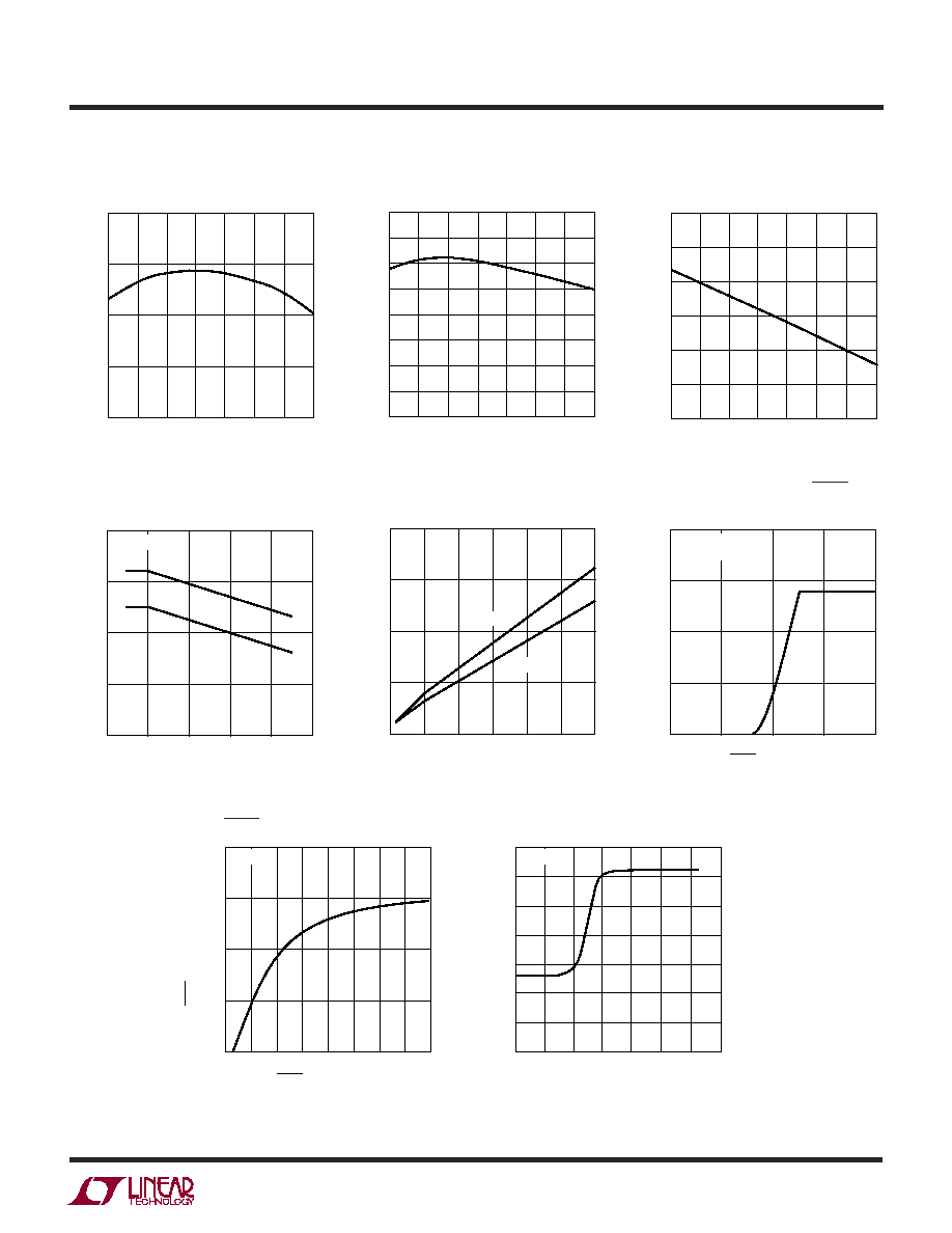
1.28
1.27
1.26
1.25
1.24
1935 G01
V
FB
(V)
TEMPERATURE (∞C)
≠50
FREQUENCY (MHz)
100
1935 G02
0
50
1.6
1.4
1.2
1.0
0.8
0.6
0.4
0.2
0
≠25
25
75
125
TEMPERATURE (∞C)
≠50
100
0
50
≠25
25
75
125
TEMPERATURE (∞C)
≠50
UVLO (V)
2.4
2.3
2.2
2.1
2.0
1.9
1.8
25
75
1935 G03
≠25
0
50
100
125
DUTY CYCLE (%)
0
CURRENT LIMIT (A)
2
3
80
1935 G04
1
0
20
40
60
100
4
SWITCH CURRENT (A)
0
SWITCH SATURATION VOLTAGE (mV)
400
300
200
100
0
0.5
1.0
1.5
2.0
1935 G05
2.5
3.0
SHDN VOLTAGE (V)
0
CURRENT LIMIT (A)
2
3
2.0
1935 G06
1
0
0.5
1.0
1.5
4
SHDN PIN VOLTAGE (V)
2
SHDN PIN CURRENT (
µ
A)
0
1935 G07
6
10
14
80
60
40
20
0
4
8
12
16
FEEDBACK VOLTAGE (V)
0
1.4
1.2
1.0
0.8
0.6
0.4
0.2
0
0.6
1.0
1935 G08
0.2
0.4
0.8
1.2
1.4
SWITCHING FREQUENCY (MHz)
T
A
= 25∞C
T
A
= 25∞C
T
A
= 25∞C
T
A
= 25∞C
T
A
= 85∞C
50% DUTY CYCLE
T
A
= 25∞C
TYP
MIN
TYPICAL PERFOR A CE CHARACTERISTICS
U
W
FB Pin Voltage
Oscillator Frequency
Undervoltage Lockout
Current Limit
Switch Saturation Voltage
Peak Switch Current vs SHDN Pin
Voltage (Soft-Start)
SHDN Pin Current
Frequency Foldback
4
LT1935
1935f
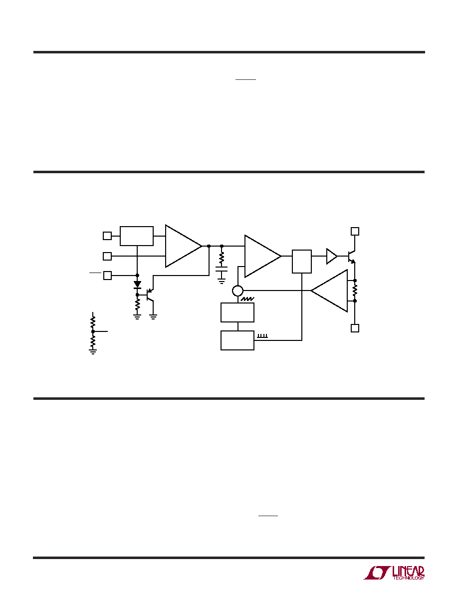
SW (Pin 1): Switch Pin. Connect inductor/diode here.
Minimize trace area at this pin to reduce EMI.
GND (Pin 2): Ground. Tie directly to local ground plane.
FB (Pin 3): Feedback Pin. Reference voltage is 1.265V.
Connect resistive divider tap here. Minimize trace area at
FB. Set V
OUT
according to V
OUT
= 1.265V(1 + R1/R2).
U
U
U
PI FU CTIO S
SHDN (Pin 4): Shutdown Pin. Tie to 1.8V or more to enable
device. Ground to shut down. This pin also provides a soft-
start function; see Applications Information section.
V
IN
(Pin 5): Input Supply Pin. Must be locally bypassed.
BLOCK DIAGRA
W
Figure 2. Block Diagram
≠
+
≠
+
R
Q
S
0.01
SW
DRIVER
COMPARATOR
2
1
V
IN
5
SHDN
4
FB
3
≠
+
RAMP
GENERATOR
1.265V
REFERENCE
R
C
C
C
1.2MHz
OSCILLATOR
GND
1935 BD
Q1
A2
A1
R1 (EXTERNAL)
R2 (EXTERNAL)
FB
V
OUT
x15
OPERATIO
U
The LT1935 uses a constant frequency, current mode
control scheme to provide excellent line and load regula-
tion. Operation can be best understood by referring to the
Block Diagram in Figure 2. At the start of each oscillator
cycle, the SR latch is set, turning on the power switch Q1.
A voltage proportional to the switch current is added to a
stabilizing ramp and the resulting sum is fed into the
positive terminal of the PWM comparator, A2. When this
voltage exceeds the level at the negative input of A2, the
SR latch is reset, turning off the power switch. The level
at the negative input of A2 is set by error amplifier A1, and
is simply an amplified version of the difference between
the feedback voltage and the reference voltage of 1.265V.
In this manner, the error amplifier sets the correct peak
current level to keep the output in regulation. If the error
amplifier's output increases, more current is delivered to
the output; if it decreases, less current is delivered. A
clamp on the output of A1 (not shown) limits the switch
current to 3A. A1's output is also clamped to the voltage
on the SHDN pin, providing a soft-start function by con-
trolling the peak switch current during start-up.
5
LT1935
1935f
APPLICATIO
N
S I
N
FOR
M
ATIO
N
W
U
U
U
Inductor Selection
Use inductors that are intended for high frequency power
applications. The saturation current rating should be at
least 2A. The RMS current rating, which is usually based
on heating of the inductor, should be higher than the
average current in the inductor in your application. For
best efficiency, the DC resistance should be less than
100m.
A good first choice for the inductor value results in a ripple
current that is 1/3 of the maximum switch current:
L = 3 (V
IN
/V
OUT
) (V
OUT
≠ V
IN
)/(I
MAX
∑ f)
I
MAX
is the maximum switch current of 2A and f is the
switching frequency. At lower duty cycles (less than 70%),
this value can be lowered somewhat in order to use a
physically smaller inductor.
Table 1 lists several inductor manufacturers, along with
part numbers for inductors that are a good match to the
LT1935.
Table 1. Inductor Suppliers
Supplier
Model Prefix
Sumida
CDRH4D18, CDRH4D28,
CDRH5D18, CDRH5D28, CR43
Coiltronics/Cooper
SD10, SD12, SD18, SD20
Wurth Elektronik
WE-PD2S, WE-PD3S, WE-PD4S
Coilcraft
MSS5131, MSS6132, DO1608
Diode Selection
Use a Schottky rectifier with a 1A or higher current rating,
such as the On Semiconductor MBRM120. Its 20V reverse
voltage rating is adequate for most applications. Higher
output voltages may require a 30V of 40V diode.
Capacitor Selection
Use capacitors with low ESR (equivalent series resis-
tance). In most cases, multilayer ceramic capacitors are
the best choice. They offer high performance (very low
ESR) in a small package. Use only X5R or X7R types; they
maintain their capacitance over temperature and applied
voltage. Other suitable capacitor types include low-ESR
tantalum capacitors that are specified for power applica-
tions, and newer types of capacitors such as Sanyo's
POSCAP and Panasonic's SP CAP.
Use a 4.7µF ceramic capacitor to bypass the input of the
LT1935. Be aware that the switching regulators require a
low impedance input supply. Additional bulk capacitance
may be required if the LT1935 circuit is more than a few
inches away from the power source. If there are low ESR
capacitors nearby, the input bypass capacitor can be
reduced to 2.2µF.
The output capacitor supports the output under transient
loads and stabilizes the control loop of the LT1935. Look
at the typical application circuits as a starting point to
choose a value. Generally, a higher output capacitance is
required at higher load currents and lower input voltages.
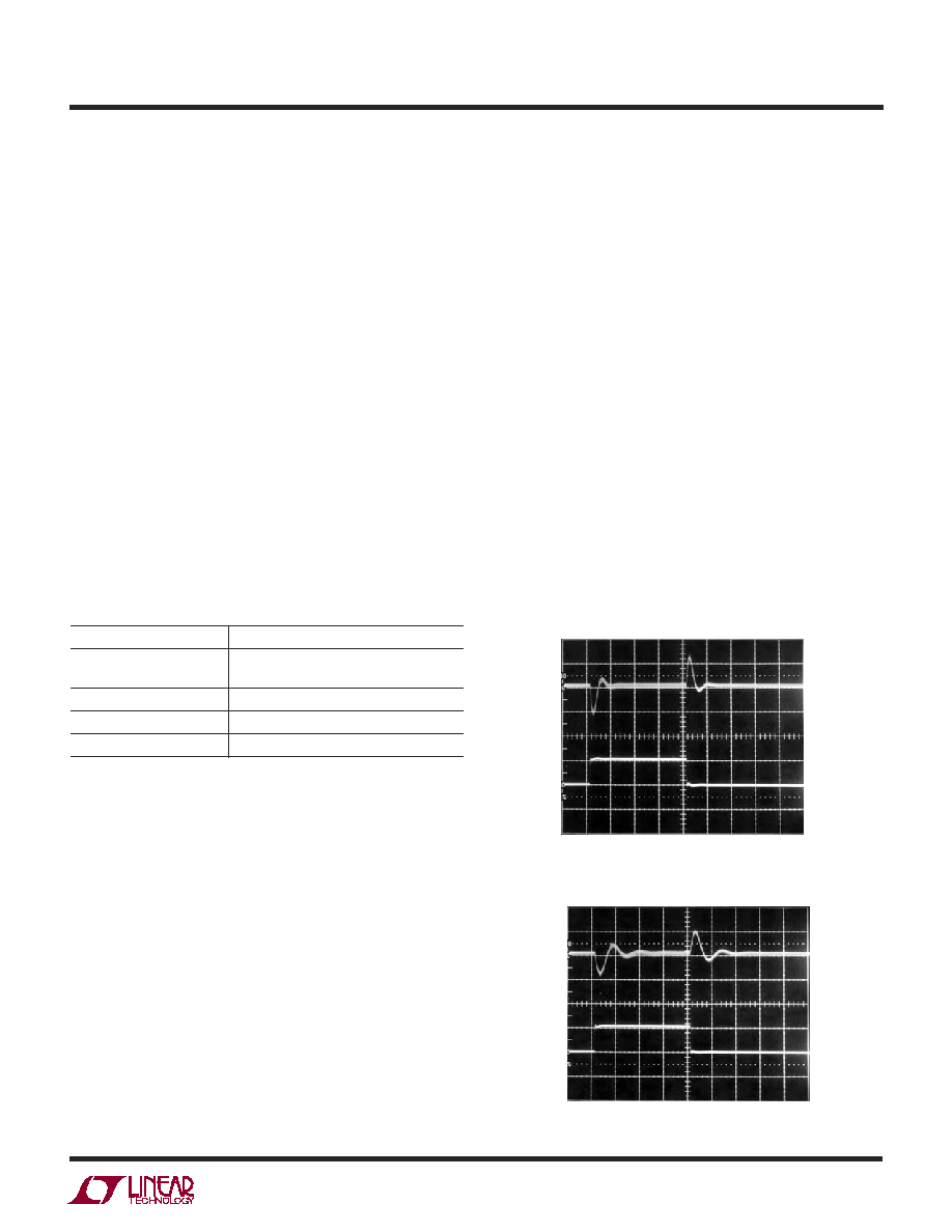
Figure 3 shows transient response of the circuit in Fig-
ure 1. The load is stepped from 200mA to 400mA and back
to 200mA. The transient performance can be improved by
increasing the output capacitance, but may require a
phase lead capacitor between the output and the FB pin.
Figure 4 shows the transient response with the output
capacitor increased to 20µF. Figure 5 shows the additional
improvement resulting from the phase lead capacitor.
Figure 4. Transient Response with C
OUT
= 20µF
Figure 3. Transient Response of the Circuit in Figure 1,
C
OUT
= 10µF
..
VOUT
100mV/DIV
ILOAD
200mA/DIV
50µs/DIV
1935 F03
0
VOUT
100mV/DIV
ILOAD
200mA/DIV
50µs/DIV
1935 F04