 | –≠–ª–µ–∫—Ç—Ä–æ–Ω–Ω—ã–π –∫–æ–º–ø–æ–Ω–µ–Ω—Ç: LTC1411IG | –°–∫–∞—á–∞—Ç—å:  PDF PDF  ZIP ZIP |
1
LTC1411
1411f
Single Supply
14-Bit 2.5Msps ADC
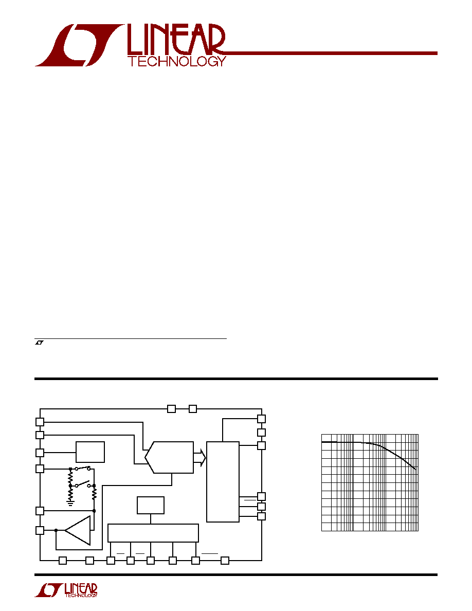
The LTC
Æ
1411 is a 2.5Msps sampling 14-bit A/D con-
verter in a 36-pin SSOP package, which typically dissi-
pates only 195mW from a single 5V supply. This device
comes complete with a high bandwidth sample-and-
hold, a precision reference, programmable input ranges
and an internally trimmed clock. The ADC can be powered
down with either the Nap or Sleep mode for low power
applications.
The LTC1411 converts either differential or single-ended
inputs and presents data in 2's complement format.
Maximum DC specs include
±
2LSB INL and 14-bit no
missing code over temperature. Outstanding dynamic
performance includes 80dB S/(N + D) and 90dB THD at
100kHz input frequency.
The LTC1411 has four programmable input ranges se-
lected by two digital input pins, PGA0 and PGA1. This
provides input spans of
±
1.8V,
±
1.27V,
±
0.9V and
±
0.64V.
An out-of-the-range signal together with the D13 (MSB)
will indicate whether a signal is over or under the ADC's
input range. A simple conversion start input and a data
ready signal ease connections to FIFOs, DSPs and micro-
processors.
s
Sample Rate: 2.5Msps
s
80dB S/(N + D) and 90dB THD at 100kHz f
IN
s
Single 5V Operation
s
No Pipeline Delay
s
Programmable Input Ranges
s
Low Power Dissipation: 195mW (Typ)
s
True Differential Inputs Reject Common Mode Noise
s
Out-of-Range Indicator
s
Internal or External Reference
s
Sleep (1
µ
A) and Nap (2mA) Shutdown Modes
s
36-Pin SSOP Package
, LTC and LT are registered trademarks of Linear Technology Corporation.
s
Telecommunications
s
High Speed Data Acquisition
s
Digital Signal Processing
s
Multiplexed Data Acquisition Systems
s
Spectrum Analysis
s
Imaging Systems
OTR
D13
OGND
DVP
OV
DD
CONTROL LOGIC
2.5V
BANDGAP
REFERENCE
INTERNAL
CLOCK
14-BIT
ADC
OUTPUT
DRIVERS
REFOUT
14
+
≠
PGA0
PGA1
CONVST
DGND
1411 BD
A
IN
+
A
IN
≠
NAP
SLP
∑
∑
∑
AVM
7, 8, 9
3
REFIN
2k
5k
5k
2
1
32
33
34
35
36
11
AGND
31
26
BUSY
27
D0
25
12
28
29
30
4
REFCOM1
5
REFCOM2
6
X1.62/
X1.15
AVP
10
FEATURES
DESCRIPTIO
U
APPLICATIO S
U
BLOCK DIAGRA
W
INPUT FREQUENCY (kHz)
10
38
S/(N + D) (dB)
EFFECTIVE BITS
50
62
100
1000
10000
1411 TA02
26
14
86
74
32
44
56
20
80
68
10
14
12
13
11
S/(N + D) and Effective Bits
vs Input Frequency
2
LTC1411
1411f
AVP = DVP = OV
DD
= V
DD
(Notes 1, 2)
Supply Voltage (V
DD
) ................................................. 6V
Analog Input Voltage (Note 3) ... ≠ 0.3V to (V
DD
+ 0.3V)
Digital Input Voltage (Note 4) .................. ≠ 0.3V to 10V
Digital Output Voltage ............... ≠ 0.3V to (V
DD
+ 0.3V)
Power Dissipation .............................................. 500mW
Operating Temperature Range
LTC1411C ............................................... 0
∞
C to 70
∞
C
LTC1411I ............................................ ≠ 40
∞
C to 85
∞
C
Storage Temperature Range ................. ≠ 65
∞
C to 150
∞
C
Lead Temperature (Soldering, 10 sec).................. 300
∞
C
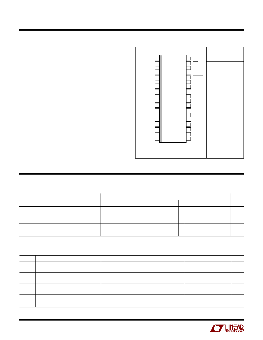
ORDER PART
NUMBER
LTC1411CG
LTC1411IG
1
2
3
4
5
6
7
8
9
10
11
12
13
14
15
16
17
18
TOP VIEW
G PACKAGE
36-LEAD PLASTIC SSOP
36
35
34
33
32
31
30
29
28
27
26
25
24
23
22
21
20
19
SLP
NAP
PGA0
PGA1
CONVST
DGND
DVP
OV
DD
OGND
BUSY
OTR
D0
D1
D2
D3
D4
D5
D6
A
IN
+
A
IN
≠
REFOUT
REFIN
REFCOM1
REFCOM2
AGND1
AGND2
AGND3
AVP
AVM
D13 (MSB)
D12
D11
D10
D9
D8
D7
T
JMAX
= 125
∞
C,
JA
= 95
∞
C/ W
temperature range, otherwise specifications are T
A
= 25
∞
C. (Notes 5, 6)
The
q
denotes specifications which apply over the full operating
PARAMETER
CONDITIONS
MIN
TYP
MAX
UNITS
Resolution (No Missing Codes)
q
14
Bits
Integral Linearity Error
(Note 7)
q
±
2
LSB
Offset Error
(Note 8)
±
16
LSB
q
±
24
LSB
Full-Scale Error
External Reference = 2.5V
±
60
LSB
Full-Scale Tempco
I
OUT(REF)
= 0
±
15
ppm/
∞
C
ACCURACY
IC
DY
U
W
A
T
A
= 25
∞
C (Note 5)
SYMBOL
PARAMETER
CONDITIONS
MIN
TYP
MAX
UNITS
S/(N + D) Signal-to-Noise Plus Distortion Ratio
100kHz Input Signal
80.0
dB
500kHz Input Signal
77.5
dB
THD
Total Harmonic Distortion
100kHz Input Signal, Up to 5th Harmonic
≠ 90
dB
500kHz Input Signal, Up to 5th Harmonic
≠ 82
dB
Peak Harmonic or Spurious Noise
100kHz Input Signal
90
dB
500kHz Input Signal
82
dB
Full Linear Bandwidth
S/(N + D)
74dB
1.0
MHz
Transition Noise
0.66
LSB
RMS
ABSOLUTE AXI U RATI GS
W
W
W
U
PACKAGE/ORDER I FOR ATIO
U
U
W
CO VERTER CHARACTERISTICS
U
Consult LTC Marketing for parts specified with wider operating temperature ranges.
3
LTC1411
1411f
SYMBOL
PARAMETER
CONDITIONS
MIN
TYP
MAX
UNITS
V
IN
Analog Input Range (Note 9)
(A
IN
+
) ≠ (A
IN
≠
), PGA0 = PGA1 = 5V
±
1.8
V
(A
IN
+
) ≠ (A
IN
≠
), PGA0 = 5V, PGA1 = 0V
±
1.27
V
(A
IN
+
) ≠ (A
IN
≠
), PGA0 = 0V, PGA1 = 5V
±
0.9
V
(A
IN
+
) ≠ (A
IN
≠
), PGA0 = PGA1 = 0V
±
0.64
V
Common Mode Input Range
A
IN
+
or A
IN
≠
0
V
DD
V
C
IN
Analog Input Capacitance
Between Conversions (Sample Mode)
10
pF
During Conversions (Hold Mode)
4
pF
t
ACQ
Sample-and-Hold Acquisition Time
100
ns
t
AP
Sample-and-Hold Aperture Delay Time
7
ns
t
jitter
Sample-and-Hold Aperture Delay Time Jitter
1
ps
RMS
CMRR
Analog Input Common Mode Rejection Ratio
0V < (A
IN
≠
= A
IN
+
) < V
DD
62
dB
Input Leakage Current (Pins 1, 2)
0.1
µ
A
PARAMETER
CONDITIONS
MIN
TYP
MAX
UNITS
V
REF
Output Voltage
I
OUT
= 0
2.480
2.500
2.520
V
V
REF
Output Tempco
I
OUT
= 0
±
15
ppm/
∞
C
V
REF
Line Regulation
4.75V
V
DD
5.25V
0.01
LSB/ V
V
REF
Load Regulation
0
I
OUT
1mA
2
LSB/mA
REFCOM2 Output Voltage
I
OUT
= 0, PGA0 = PGA1 = 5V
4.05
V
REFIN Input Current
REFIN = External Reference 2.5V
250
µ
A
SYMBOL
PARAMETER
CONDITIONS
MIN
TYP
MAX
UNITS
V
IH
High Level Input Voltage
V
DD
= 5.25V
q
2.4
V
V
IL
Low Level Input Voltage
V
DD
= 4.75V
q
0.8
V
I
IN
Digital Input Current
V
IN
= 0V to V
DD
, Except SLP, NAP (Note 11)
q
±
10
µ
A
C
IN
Digital Input Capacitance
2
pF
V
OH
High Level Output Voltage
V
DD
= 4.75V, I
O
= ≠ 10
µ
A
4.75
V
V
DD
= 4.75V, I
O
= ≠ 200
µ
A
q
4.0
V
V
OL
Low Level Output Voltage
V
DD
= 4.75V, I
O
= 160
µ
A
0.05
V
V
DD
= 4.75V, I
O
= 1.6mA
q
0.10
0.4
V
I
SOURCE
Output Source Current
V
OUT
= 0V
≠ 10
mA
I
SINK
Output Sink Current
V
OUT
= V
DD
10
mA
The
q
denotes specifications which apply over the full operating temperature range, otherwise specifications are T
A
= 25
∞
C. (Note 5)
SYMBOL
PARAMETER
CONDITIONS
MIN
TYP
MAX
UNITS
V
DD
Supply Voltage
(Note 9)
4.75
5.25
V
I
DD
Supply Current
q
39
65
mA
Nap Mode
NAP = 0V (Note 11)
2
mA
Sleep Mode
SLP = 0V
1
µ
A
P
D
Power Dissipation
q
195
325
mW
Nap Mode
NAP = 0V
10
mW
Sleep Mode
SLP = 0V
5
µ
W
The
q
denotes specifications which apply over the full operating temperature range, otherwise specifications are T
A
= 25
∞
C. (Note 5)
T
A
= 25
∞
C (Note 5)
T
A
= 25
∞
C (Note 5)
A ALOG I PUT
U
U
I TER AL REFERE CE CHARACTERISTICS
U
U
U
DIGITAL I PUTS A D DIGITAL OUTPUTS
U
U
POWER REQUIRE E TS
W
U
4
LTC1411
1411f
TI I G CHARACTERISTICS
W U
range, otherwise specifications are T
A
= 25
∞
C. (Notes 5) (See Figures 11a, 11b)
The
q
denotes specifications which apply over the full operating temperature
SYMBOL
PARAMETER
CONDITIONS
MIN
TYP
MAX
UNITS
f
SAMPLE(MAX)
Maximum Sampling Frequency
(Note 9)
q
2.5
MHz
t
CONV
Conversion Time
q
250
350
ns
t
ACQ
Acquisition Time
100
ns
t
0
SLP
to CONVST
Wake-Up Time
10
µ
F Bypass Capacitor at REFCOM2 Pin
210
ms
t
1
NAP
to CONVST
Wake-Up Time
250
ns
t
2
CONVST
Low Time
(Note 10)
q
20
ns
t
3
CONVST to BUSY Delay
C
L
= 25pF
12
ns
t
4
Data Ready After BUSY
7
ns
t
5
CONVST High Time
(Note 10)
q
20
ns
t
6
Aperture Delay of Sample-and-Hold
7
ns
Note 1: Absolute Maximum Ratings are those values beyond which the life
of a device may be impaired.
Note 2: All voltage values are with respect to ground with DGND, OGND,
AVM and AGND wired together unless otherwise noted.
Note 3: When these pin voltages are taken below AGND or above V
DD
,
they will be clamped by internal diodes. This product can handle input
currents greater than 100mA without latchup.
Note 4: When these pin voltages are taken below AGND, they will be
clamped by internal diodes. This product can handle input currents greater
than 100mA below AGND without latchup. These pins are not clamped to
V
DD
.
Note 5: V
DD
= 5V, PGA1 = PGA0 = 5V, f
SAMPLE
= 2.5MHz at 25
∞
C and
t
r
= t
f
= 5ns unless otherwise specified.
Note 6: Linearity, offset and full-scale specifications apply for a single-
ended A
IN
+
input with A
IN
≠
tied to an external 2.5V reference voltage.
Note 7: Integral nonlinearity is defined as the deviation of a code from a
straight line passing through the actual endpoints of the transfer curve.
The deviation is measured from the center of the quantization band.
Note 8: Bipolar offset is the offset voltage measured from ≠ 0.5LSB
when the output code flickers between 0000 0000 0000 00 and
1111 1111 1111 11.
Note 9: Recommended operating conditions.
Note 10: The falling CONVST edge starts a conversion. If CONVST returns
high at a critical point during the conversion it can create small errors. For
best performance ensure that CONVST returns high within 20ns after
conversion start of after BUSY rises.
Note 11: SLP and NAP have an internal pull-down so the pins will draw
approximately 7
µ
A when tied high and less than 1
µ
A when tied low.
TYPICAL PERFOR A CE CHARACTERISTICS
U
W
Signal-to-Noise Ratio
vs Input Frequency
INPUT FREQUENCY (kHz)
10
38
S/(N + D) (dB)
50
62
100
1000
10000
1411 G01
26
14
86
74
32
44
56
20
80
68
INPUT FREQUENCY (kHz)
10
38
SNR (dB)
50
62
100
1000
10000
1411 G02
26
14
86
74
32
44
56
20
80
68
INPUT FREQUENCY (kHz)
10
≠80
DISTORTION (dB)
≠60
≠40
100
1000
10000
1411 G03
≠100
≠110
0
≠20
≠90
≠70
≠50
≠10
≠30
2ND
3RD
THD
S/(N + D) vs Input Frequency
Distortion vs Input Frequency
5
LTC1411
1411f
TYPICAL PERFOR A CE CHARACTERISTICS
U
W
INPUT FREQUENCY (kHz)
10
≠80
DISTORTION (dB)
≠60
≠40
100
1000
10000
1411 G04
≠100
≠110
0
≠20
≠90
≠70
≠50
≠10
≠30
Spurious Free Dynamic Range
vs Input Frequency
S/(N + D) vs Input Frequency
and Amplitude
Integral Nonlinearity
vs Output Code
Differential Nonlinearity
vs Output Code
INPUT FREQUENCY (kHz)
10
38
SINAD (dB)
50
62
100
1000
10000
1411 G05
26
14
86
74
32
44
56
20
80
68
0dB
≠20dB
≠40dB
OUTPUT CODE
0
≠1.0
INL (LSB)
≠0.8
≠0.4
≠0.2
0
1.0
0.4
4096
8192
1411 G07
≠0.6
0.6
0.8
0.2
12288
16384
OUTPUT CODE
0
≠1.0
DNL (LSB)
≠0.8
≠0.4
≠0.2
0
1.0
0.4
4096
8192
1411 G08
≠0.6
0.6
0.8
0.2
12288
16384
Supply Current vs Temperature
TEMPERATURE (
∞
C)
≠50
45
44
43
42
41
40
39
38
37
36
35
SUPPLY CURRENT (mA)
≠25
0
25
50
1411 G11
75
100
V
DD
= 5V
Supply Current vs Supply Voltage
V
DD
(V)
4.5
31.5
SUPPLY CURRENT (mA)
34.0
36.5
39.0
41.5
44.0
46.5
T
A
= 25
∞
C
4.75
5.0
5.25
5.5
1411 G12
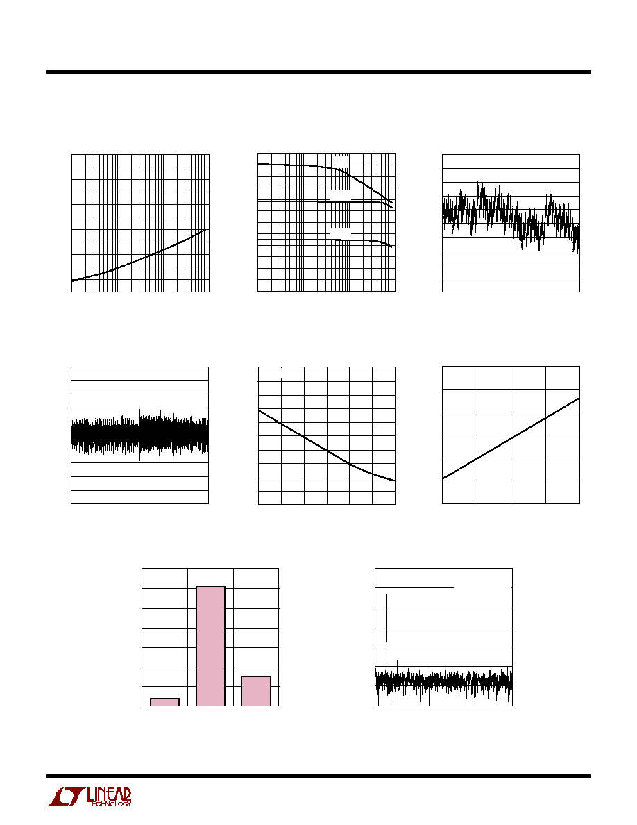
Histogram for 4096 Conversions
CODE
3500
3000
2500
2000
1500
1000
500
0
0
1
1411 G13
≠1
COUNTS
4096 Points FFT Plot (100kHz)
INPUT FREQUENCY (kHz)
0
≠60
≠40
0
1411 G14
≠80
≠100
≠120
≠140
≠20
AMPLITUDE (dB)
SINAD = 78.8dB
SFDR = 95dB
f
SAMPLE
= 2.5MHz
f
IN
= 100kHz
1000
250
500
750
1250