1
LTC3423/LTC3424
34234f
The LTC
Æ
3423 and LTC3424 are high efficiency, fixed
frequency, step-up DC/DC converters that can regulate
output voltages as low as 1.5V from a single cell. An
applied voltage of at least 2.7V to the V
DD
pin is required
to power the internal control circuitry.
The devices include a 0.16
N-channel MOSFET switch
and a 0.21
P-channel synchronous rectifier. The LTC3423
is intended for applications requiring less than 0.75W of
output power and the LTC3424 for 1.5W or less. Switching
frequencies up to 3MHz are programmed with an external
timing resistor and the oscillator can be synchronized to
an external clock.
Quiescent current is only 38
µ
A in Burst Mode operation,
maximizing battery life in portable applications. Burst
Mode operation is user controlled and can be enabled by
driving the MODE/SYNC pin high. If the MODE/SYNC pin
has either a clock or is driven low then the operation is at
constant fixed frequency.
Other features include a 1
µ
A shutdown, thermal shutdown
and current limit. The LTC3423 and LTC3424 are available
in the 10-lead MSOP package. For applications requiring
an output voltage greater than 2.6V, the LTC3401 and
LTC3402 are recommended without the need of a separate
voltage for the V
DD
pin.
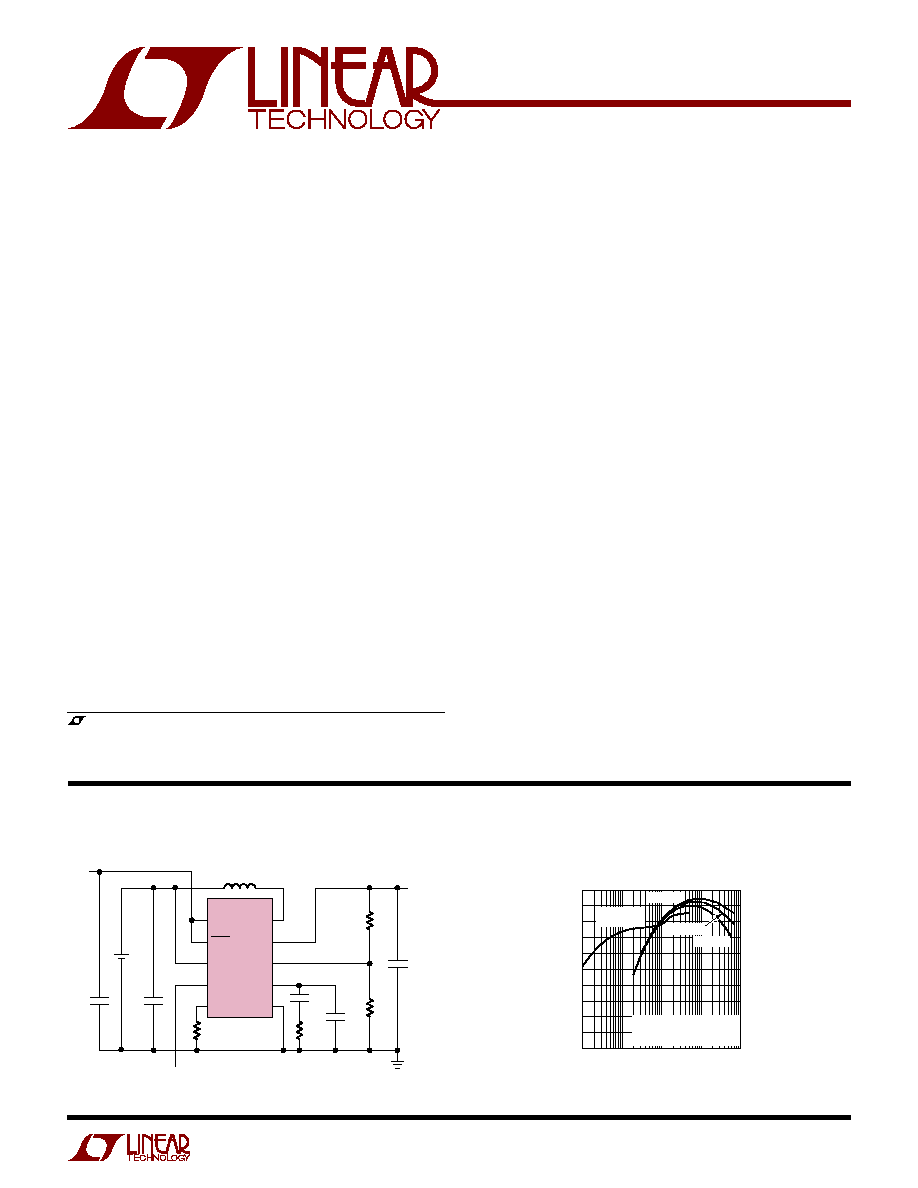
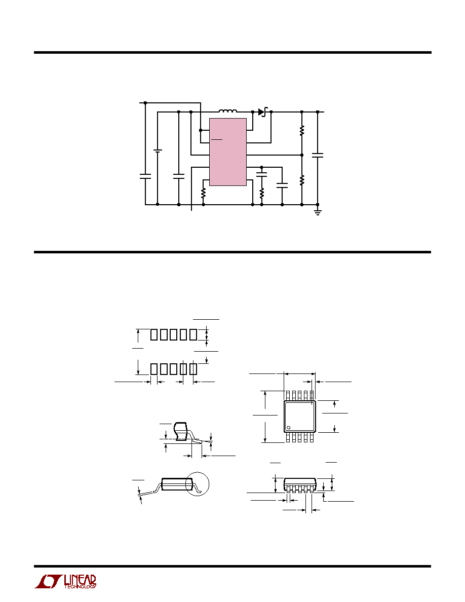
1-Cell to 1.8V at 600mA Step-Up Converter
s
Pagers
s
Handheld Instruments
s
Cordless Phones
s
Wireless Handsets
s
GPS Receivers
s
Battery Backup
s
1.5V to 5.5V Adjustable Output Voltage
s
Synchronous Rectification: Up to 95% Efficiency
s
1A Switch Current (LTC3423) or
2A Switch Current (LTC3424)
s
Fixed Frequency Operation Up to 3MHz
s
Wide Input Range: 0.5V to 5.5V (Operating)
s
Very Low Quiescent Current: 38
µ
A (Burst Mode
Æ
Operation)
s
No External Schottky Diode Required
s
Synchronizable Switching Frequency
s
Burst Mode Enable Control
s
OPTI-LOOP
Æ
Compensation
s
Very Low Shutdown Current: < 1
µ
A
s
Small 10-Pin MSOP Package
, LTC and LT are registered trademarks of Linear Technology Corporation.
Burst Mode and OPTI-LOOP are registered trademarks of Linear Technology Corporation.
Efficiency
Low Output Voltage,
3MHz Micropower Synchronous
Boost Converters
DESCRIPTIO
U
FEATURES
APPLICATIO S
U
TYPICAL APPLICATIO
U
6
10
3
2
1
LTC3424
V
DD
SHDN
V
IN
MODE/SYNC
R
t
SW
V
OUT
FB
V
C
GND
4
7
8
9
5
C4
470pF
C2
10
µ
F
RC
82k
R
t
30.1k
R1
110k
R2
249k
L1
2.2
µ
H
C3
44
µ
F
(2
◊
22
µ
F)
C1: TAIYO YUDEN JMK212BJ225MG
C2: TAIYO YUDEN JMK212BJ106MM
C3: TAIYO YUDEN JMK325BJ226MM
L1: SUMIDA CD43-2R2M
V
DD
= 2.7V TO 5.5V
V
IN
= 0.9V TO 1.5V
0 = FIXED FREQ
1 = Burst Mode OPERATION
C5
4.7pF
3423/24 TA01
V
OUT
1.8V
600mA
1
CELL
V
DD
+
≠
C1
2.2
µ
F
3223/24 TA02
Burst Mode
OPERATION
V
IN
= 1.5V
V
DD
= 3.3V
V
OUT
= 1.8V
WITH MBRM120T3 SCHOTTKY
V
IN
= 0.9V
OUTPUT CURRENT (mA)
EFFICIENCY (%)
100
90
80
70
60
50
40
30
20
10
0
0.1
10
100
1000
1
V
IN
= 1.2V
2
LTC3423/LTC3424
34234f
PARAMETER
CONDITIONS
MIN
TYP
MAX
UNITS
V
DD
Input Voltage Range
q
2.7
5.5
V
V
IN
Operating Voltage Range
(Note 4)
q
0.5
5.5
V
Output Voltage Adjust Range
q
1.5
5.5
V
Feedback Voltage
q
1.22
1.25
1.28
V
Feedback Input Current
V
FB
= 1.25V
1
50
nA
Quiescent Current--Burst Mode Operation
V
C
= 0V, MODE/SYNC = 3.3V (Note 3)
38
65
µ
A
Quiescent Current--SHDN
SHDN = 0V, Not Including Switch Leakage
0.1
1
µ
A
Quiescent Current--Active
V
C
= 0V, MODE/SYNC = 0V, R
t
= 300k (Note 3)
440
800
µ
A
NMOS Switch Leakage
0.1
5
µ
A
PMOS Switch Leakage
0.1
10
µ
A
NMOS Switch On Resistance
0.16
PMOS Switch On Resistance
0.21
NMOS Current Limit
LTC3423
q
1
1.6
A
LTC3424
q
2
2.8
A
Maximum Duty Cycle
R
t
= 15k
q
80
85
%
Minimum Duty Cycle
q
0
%
Frequency Accuracy
R
t
= 15k
q
1.6
2
2.4
MHz
MODE/SYNC Input High
1.4
V
MODE/SYNC Input Low
0.4
V
MODE/SYNC Input Current
V
MODE/SYNC
= 5.5V
0.01
1
µ
A
Error Amp Transconductance
I = ≠ 5
µ
A to 5
µ
A, V
C
= V
FB
85
µ
mhos
(Note 1)
V
IN
, V
OUT
, V
DD
Voltages .............................. ≠ 0.5V to 6V
SW Voltage ................................................. ≠ 0.5V to 6V
V
C
, R
t
Voltages ......................... ≠ 0.5V to (V
OUT
+ 0.3V)
SHDN, FB, MODE Voltages ......................... ≠ 0.5V to 6V
Operating Temperature Range (Note 2) .. ≠ 40
∞
C to 85
∞
C
Storage Temperature Range ................. ≠ 65
∞
C to 125
∞
C
Lead Temperature (Soldering, 10 sec).................. 300
∞
C
T
JMAX
= 125
∞
C
JA
= 130
∞
C/ W 1 LAYER BOARD
JA
= 100
∞
C/ W 4 LAYER BOARD
MS PART MARKING
ORDER PART
NUMBER
LTC3423EMS
LTC3424EMS
LTQM
LTQN
The
q
denotes specifications that apply over the full operating temperature range, otherwise specifications are at T
A
= 25
∞
C.
V
IN
= 1.2V, V
DD
= 3.3V, V
OUT
= 1.8V, unless otherwise noted.
ABSOLUTE AXI U RATI GS
W
W
W
U
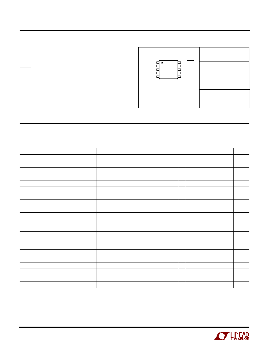
PACKAGE/ORDER I FOR ATIO
U
U
W
ELECTRICAL CHARACTERISTICS
Consult LTC Marketing for parts specified with wider operating temperature ranges.
1
2
3
4
5
R
t
MODE
V
IN
SW
GND
10
9
8
7
6
SHDN
V
C
FB
V
OUT
V
DD
TOP VIEW
MS PACKAGE
10-LEAD PLASTIC MSOP
3
LTC3423/LTC3424
34234f
The
q
denotes specifications that apply over the full operating temperature range, otherwise specifications are at T
A
= 25
∞
C.
V
IN
= 1.2V, V
OUT
= 3.3V unless otherwise noted.
PARAMETER
CONDITIONS
MIN
TYP
MAX
UNITS
SHDN Input High
V
SHDN
= V
IN
= V
OUT
1
V
SHDN Input Low
0.4
V
SHDN Input Current
V
SHDN
= 5.5V
0.01
1
µ
A
ELECTRICAL CHARACTERISTICS
Note 1: Absolute Maximum Ratings are those values beyond which the life
of a device may be impaired.
Note 2: The LTC3423/LTC3424 are guaranteed to meet performance
specifications from 0
∞
C to 70
∞
C. Specifications over the ≠40
∞
C to 85
∞
C
operating temperature range are assured by design, characterization and
correlation with statistical process controls.
Note 3: Current is measured into V
DD
since the supply current is
bootstrapped to the V
DD
pin. The outputs are not switching.
Note 4: Once the output is started, the IC is not dependant upon the V
IN
supply.
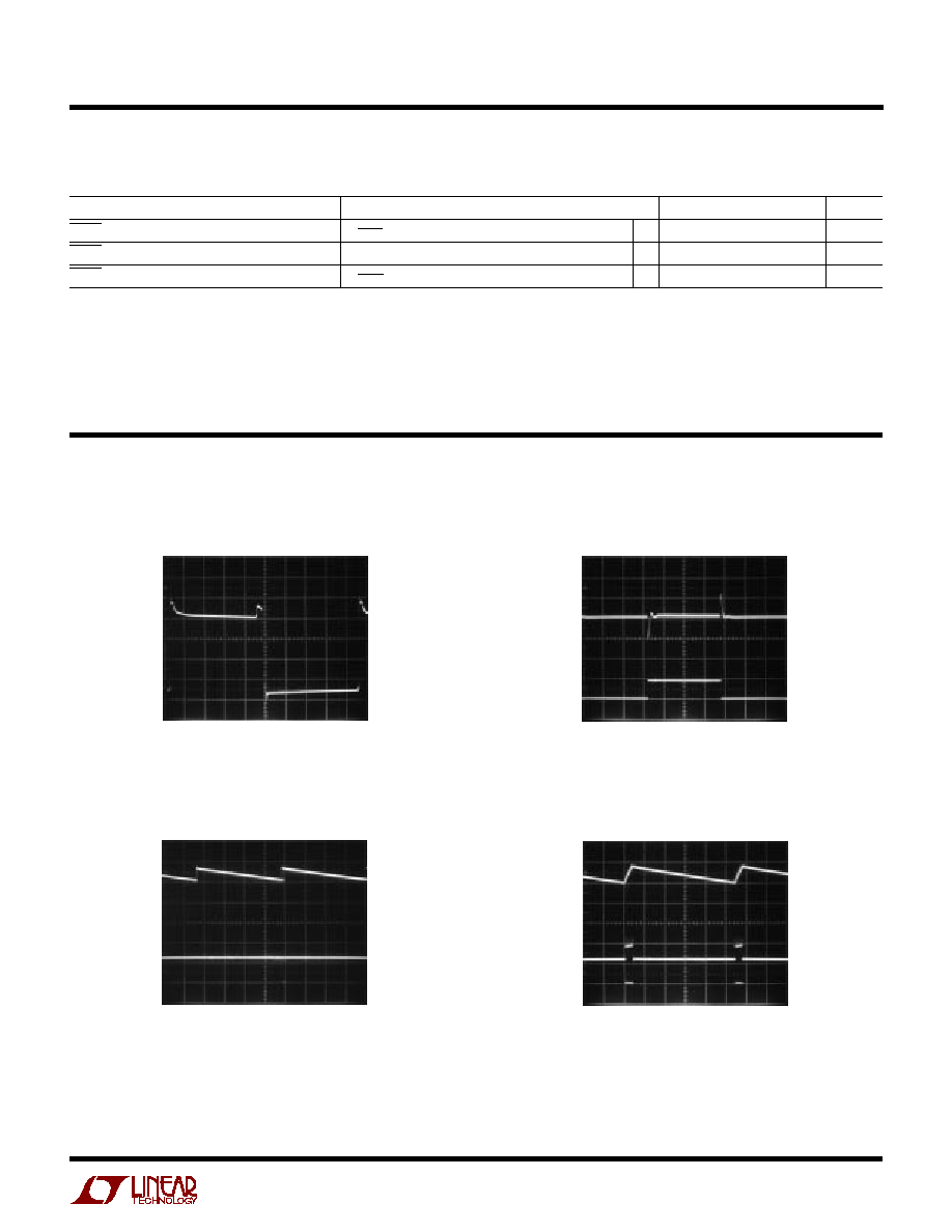
Switching Waveform on SW Pin
TYPICAL PERFOR A CE CHARACTERISTICS
U
W
Transient Response
150mA to 450mA
SW
0.5V/DIV
I
LOAD
= 500mA
100ns/DIV
3423/24 G01
V
OUT
1.8V
I
OUT
C
OUT
= 44
µ
F
200
µ
s/DIV
3423/24 G02
L = 2.2
µ
H
f
OSC
= 1MHz
V
OUT
100mV/DIV
AC COUPLED
450mA
150mA
Burst Mode Operation
at 500
µ
A Load
Burst Mode Operation
at 10mA Load
V
OUT
100mV/DIV
AC COUPLED
V
IN
= 1.2V
1ms/DIV
3423/24 G03
V
OUT
= 1.8V
C
OUT
= 44
µ
F
MODE/SYNC PIN = HIGH
SW
1V/DIV
V
OUT
100mV/DIV
AC COUPLED
V
IN
= 1.2V
500
µ
s/DIV
3423/24 G04
V
OUT
= 1.8V
C
OUT
= 44
µ
F
MODE/SYNC PIN = HIGH
SW
1V/DIV
0V
4
LTC3423/LTC3424
34234f
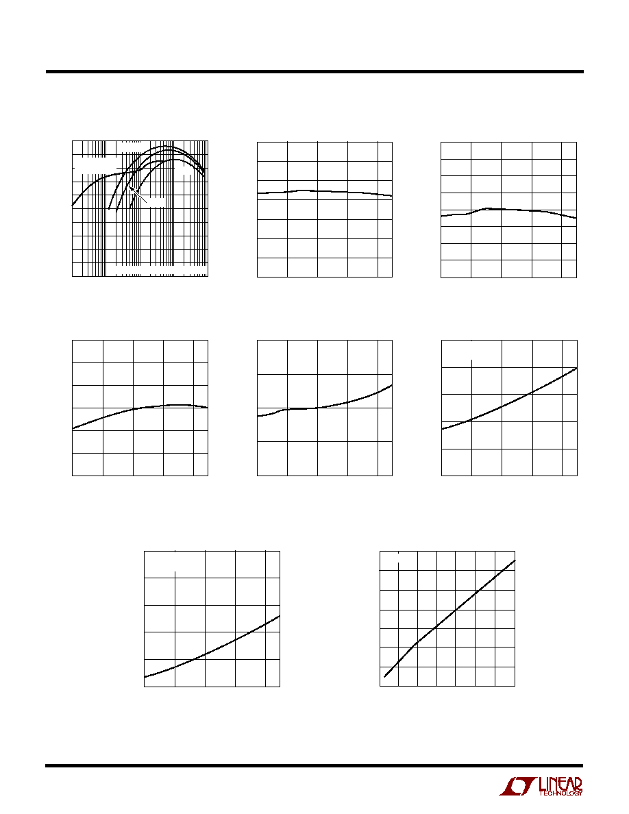
TYPICAL PERFOR A CE CHARACTERISTICS
U
W
Converter Efficiency 1.2V to 1.8V
Efficiency Loss Without Schottky
vs Frequency
LTC3423 Current Limit
EA FB Voltage
Oscillator Frequency Accuracy
PMOS R
DS(ON)
NMOS R
DS(ON)
LTC3424 Current Limit
OUTPUT CURRENT (mA)
EFFICIENCY (%)
100
90
80
70
60
50
40
30
20
10
0
0.1
10
100
1000
3223/24 G05
1
Burst Mode
OPERATION
300MHz
WITH MBRM120T3 SCHOTTKY
3MHz
1MHz
TEMPERATURE (
∞
C)
≠55
CURRENT (A)
2.6
2.8
3.0
65
125
3423/24 G06
2.4
2.2
2.0
≠15
25
105
3.2
3.4
TEMPERATURE (
∞
C)
≠55
CURRENT (A) 1.55
1.60
1.65
65
125
3423/24 G07
1.50
1.45
1.40
≠15
25
105
1.70
1.75
1.80
TEMPERATURE (
∞
C)
≠55
VOLTAGE (V)
1.23
1.24
1.25
65
125
3423/24 G08
1.22
≠15
25
105
1.26
1.27
1.28
TEMPERATURE (
∞
C)
≠55
FREQUENCY (MHz)
2.00
65
125
3423/24 G09
1.95
1.90
≠15
25
105
2.05
2.10
R
T
= 15k
TEMPERATURE (
∞
C)
≠55
RESISTANCE (
)
0.15
65
125
3423/24 G10
0.10
0.05
≠15
25
105
0.20
0.25
0.30
V
OUT
= 1.8V
V
DD
= 3.3V
TEMPERATURE (
∞
C)
≠55
RESISTANCE (
)
0.25
65
125
3423/24 G11
0.20
0.15
≠15
25
105
0.30
0.35
0.40
V
OUT
= 1.8V
V
DD
= 3.3V
FREQUENCY (MHz)
0.2
8
10
14
1.4
2.2
3423/24
G12
6
4
0.6
1.0
1.8
2.6
3.0
2
0
12
EFFICIENCY LOSS (%)
T
A
= 25
∞
C
5
LTC3423/LTC3424
34234f
TYPICAL PERFOR A CE CHARACTERISTICS
U
W
Burst Mode Operation Current
R
t
(Pin 1): Timing Resistor to Program the Oscillator
Frequency.
f
R
Hz
OSC
t
=
3 10
10
∑
MODE/SYNC (Pin 2): Burst Mode Select and Oscillator
Synchronization.
MODE/SYNC = High. Enable Burst Mode operation. The
inductor peak inductor current will be 400mA and
return to zero current on each cycle. During Burst Mode
operation the operation is variable frequency, providing
a significant efficiency improvement at light loads. It is
recommended the Burst Mode operation only be en-
tered once the part has started up.
MODE/SYNC = Low. Disable Burst Mode operation and
maintain low noise, constant frequency operation.
MODE/SYNC = External CLK. Synchronization of the
internal oscillator and Burst Mode operation disable. A
clock pulse width of 100ns to 2
µ
s is required to
synchronize.
V
IN
(Pin 3): Voltage Sense for Internal Circuitry.
U
U
U
PI FU CTIO S
SW (Pin 4): Switch Pin. Connect inductor and optional
Schottky diode here. Minimize trace length to keep EMI
down.
GND (Pin 5): Signal and Power Ground for the IC.
V
DD
(Pin 6): Power Source for the IC. Typically derived
from a higher voltage power converter. Requires an input
of 2.7V to 5.5V. A 2.2
µ
F ceramic bypass capacitor is
recommended as close to the pins as possible.
V
OUT
(Pin 7): Output of the Synchronous Rectifier.
FB (Pin 8): Feedback Pin. Connect resistor divider tap
here. The output voltage can be adjusted from 1.5V to
5.5V. The feedback reference voltage is typically 1.25V.
V
C
(Pin 9): Error Amp Output. A frequency compensation
network is connected to this pin to compensate the loop.
See the section "Compensating the Feedback Loop" for
guidelines.
SHDN (Pin 10): Shutdown. Grounding this pin shuts down
the IC. Tie to >1V to enable (V
DD
or digital gate output).
During shutdown the output voltage will hold up to V
IN
minus a diode drop due to the body diode of the PMOS
synchronous switch. If the application requires a com-
plete disconnect during shutdown then refer to section
"Output Disconnect".
Shutdown Threshold
TEMPERATURE (
∞
C)
≠55
VOLTAGE (V) 0.80
65
125
3423/24 G13
0.70
0.60
≠15
25
105
0.90
1.00
1.10
0.75
0.65
0.85
0.95
1.05
TEMPERATURE (
∞
C)
≠55
CURRENT (
µ
A)
36
38
65
125
3423/24 G14
34
32
30
≠15
25
105
40
42
44

6
LTC3423/LTC3424
34234f
BLOCK DIAGRA
W
1
≠
+
CURRENT
COMP
CURRENT
LIMIT
≠
+
ERROR
AMP
FB
R1
R2
1.25V
V
C
1.6A TYP (LTC3423)
2.8A TYP (LTC3424)
≠
+
≠
+
Burst Mode
CONTROL
+
≠
PWM
LOGIC
ANTICROSS
CONDITION
SLOPE COMP
OSC
SYNC
R
t
GND
SLEEP
8
V
OUT
V
OUT
1.5V TO 5.5V
7
4
9
MODE/SYNC
3423/24 BD
2
N
SW
10mV
1V TO
V
OUT
+ 0.3
+
V
IN
P
OPTIONAL
3
+
5
V
DD
6
SHDN
SHUTDOWN
10
I
SENSE
AMP
I
ZERO
AMP
≠
+
V
DD
2.7V TO 5.5V

7
LTC3423/LTC3424
34234f
APPLICATIO S I FOR ATIO
W
U
U
U
Zero Current Amp. The zero current amplifier monitors the
inductor current to the output and shuts off the synchro-
nous rectifier once the current is below 50mA, preventing
negative inductor current.
Burst Mode Operation
Burst Mode operation is when the IC delivers energy to the
output until it is regulated and then goes into a sleep mode
where the outputs are off and the IC is consuming only
38
µ
A. In this mode, the output ripple has a variable
frequency component with load current and the steady
state ripple will be typically below 3%.
During the period where the device is delivering energy to
the output, the peak current will be equal to 400mA and the
inductor current will terminate at zero current for each cycle.
In this mode the maximum output current is given by:
I
V
V
Amps
OUT MAXBURST
IN
OUT
(
)
∑
6
Burst Mode operation is user controlled by driving the
MODE/SYNC pin high to enable and low to disable. It is
recommended that Burst Mode operation be entered after
the part has started up.
COMPONENT SELECTION
Inductor Selection
The high frequency operation of the LTC3423/LTC3424
allows the use of small surface mount inductors. The
minimum inductance value is proportional to the operat-
ing frequency and is limited by the following constraints:
L
k
f
H and L
V
V
V
f Ripple V
H
IN MIN
OUT MAX
IN MIN
OUT MAX
> µ
>
(
)
(
)
(
)
(
)
(
)
∑
≠
∑
∑
where
k = 3 for LTC3423, 2 for LTC3424
f = Operating Frequency (Hz)
Ripple = Allowable Inductor Current Ripple (A)
V
IN(MIN)
= Minimum Input Voltage (V)
V
OUT(MAX)
= Maximum Output Voltage (V)
DETAILED DESCRIPTION
The LTC3423/LTC3424 provides high efficiency, low noise
power for applications such as portable instrumentation
and are ideal for applications that require an output voltage
between 1.5V and 2.6V from a single cell. These products
are an addition to the LTC3401 and LTC3402 family of
synchronous boost converters, with the differences being
the omission of the power good function (PGOOD) and the
addition of a V
DD
input to provide internal power. The IC
will not start up until the applied voltage on the V
DD
pin is
above 2.7V.
The current mode architecture with adaptive slope
compensation provides ease of loop compensation with
excellent transient load response. The low R
DS(ON)
, low
gate charge synchronous switches provides the pulse
width modulation control at high efficiency.
Low Noise Fixed Frequency Operation
Oscillator. The frequency of operation is set through a
resistor from the R
t
pin to ground where f = 3 ∑ 10
10
/R
t
. An
internally trimmed timing capacitor resides inside the IC.
The oscillator can be synchronized with an external clock
inserted on the MODE/SYNC pin. When synchronizing the
oscillator, the free running frequency must be set to
approximately 30% lower than the desired synchronized
frequency. Keeping the sync pulse width below 2
µ
s will
ensure that Burst Mode operation is disabled.
Current Sensing. Lossless current sensing converts the
peak current signal to a voltage to sum in with the internal
slope compensation. This summed signal is compared to
the error amplifier output to provide a peak current control
command for the PWM. The slope compensation in the IC
is adaptive to the input and output voltage. Therefore, the
converter provides the proper amount of slope compensa-
tion to ensure stability and not an excess causing a loss of
phase margin in the converter.
Error Amp. The error amplifier is a transconductance
amplifier with g
m
= 85
µ
mhos. A simple compensation
network is placed from the V
C
pin to ground.
Current Limit. The current limit amplifier will shut the
NMOS switch off once the current exceeds its threshold.
The current amplifier delay to output is typically 50ns.
8
LTC3423/LTC3424
34234f
APPLICATIO S I FOR ATIO
W
U
U
U
The inductor current ripple is typically set to 20% to 40%
of the maximum inductor current.
For high efficiency, choose an inductor with a high fre-
quency core material, such as ferrite, to reduce core
losses. The inductor should have low ESR (equivalent
series resistance) to reduce the I
2
R losses and must be
able to handle the peak inductor current at full load without
saturating. Molded chokes or chip inductors usually do
not have enough core to support the peak inductor cur-
rents in the 1A to 2A region. To minimize radiated noise,
use a toroid, pot core or shielded bobbin inductor. See
Table 1 for a list of component suppliers.
Figure 1. Recommended Component Placement. Traces
Carrying High Current Are Direct. Trace Area FB and V
C
Pins
Are Kept Low. Lead Length to Battery Should be Kept Short
where
I
L
= Average Inductor Current
I
P
= Peak Inductor Current
The ESR is usually the most dominant factor for ripple in
most power converters. The ripple due to capacitor ESR is
simply given by:
VR
CESR
= I
P
∑ R
ESR
Volts
where
R
ESR
= Capacitor Series Resistance
Low ESR capacitors should be used to minimize output
voltage ripple. For surface mount applications, AVX TPS
series tantalum capacitors and Sanyo POSCAP or Taiyo-
Yuden ceramic capacitors are recommended. For through-
hole applications Sanyo OS-CON capacitors offer low ESR
in a small package size. See Table 2 for a list of component
suppliers.
In some layouts it may be required to place a 1
µ
F low ESR
capacitor as close to the V
OUT
and GND pins as possible.
Table 1. Inductor Vendor Information
SUPPLIER
PHONE
FAX
WEBSITE
Coilcraft
(847) 639-6400
(847) 639-1469
www.coilcraft.com
Coiltronics
(516) 241-7876
(516) 241-9339
www.coiltronics.com
Murata
(814) 237-1431
(814) 238-0490
www.murata.com
(800) 831-9172
Sumida
USA: (847) 956-0666
(847) 956-0702
www.japanlink.com
Japan: 81-3-3607-5111 81-3-3607-5144
sumida
V
OUT
3423/24 F01
R
t
MODE
V
IN
SW
GND
SHDN
V
C
FB
V
OUT
V
DD
V
DD
IN
2.7V
TO 5.5V
Output Capacitor Selection
The output voltage ripple has several components. The
bulk value of the capacitor is set to reduce the ripple due
to charge into the capacitor each cycle. The max ripple due
to charge is given by:
VR
I
V V
V
C
V
V
f
BULK
L
IN OUT
IN
OUT
OUT
OUT
=
∑
(
≠
)
∑
∑
∑
Volts
Table 2. Capacitor Vendor Information
SUPPLIER
PHONE
FAX
WEBSITE
AVX
(803) 448-9411
(803) 448-1943
www.avxcorp.com
Sanyo
(619) 661-6322
(619) 661-1055
www.sanyovideo.com
Taiyo Yuden
(408) 573-4150
(408) 573-4159
www.t-yuden.com
Input Capacitor Selection
The input filter capacitor reduces peak currents drawn from
the input source and reduces input switching noise. In most
applications a 3.3
µ
F is sufficient.
Output Diode
The Schottky diode across the synchronous PMOS switch
is not required, but provides a lower drop during the break-
before-make time (typically 20ns) of the NMOS to PMOS
transition. The addition of the Schottky diode will improve
peak efficiency (see graph "Efficiency Loss Without
Schottky vs Frequency"). Use of a Schottky diode such as
a MBRM120T3, 1N5817 or equivalent. Since slow recov-
ery times will compromise efficiency, do not use ordinary
rectifier diodes.
9
LTC3423/LTC3424
34234f
Operating Frequency Selection
There are several considerations in selecting the operat-
ing frequency of the converter. The first is determining the
sensitive frequency bands that cannot tolerate any spec-
tral noise. For example, in products incorporating RF
communications, the 455kHz IF frequency is sensitive to
any noise, therefore switching above 600kHz is desired.
Some communications have sensitivity to 1.1MHz. In this
case, converter frequencies up to 3MHz may be em-
ployed.
The second consideration is the physical size of the
converter. As the operating frequency goes up, the induc-
tor and filter caps go down in value and size. The trade off
is in efficiency since the switching losses due to gate
charge are going up proportional with frequency.
Another operating frequency consideration is whether the
application can allow "pulse skipping." In this mode, the
minimum on time of the converter cannot support the duty
cycle, so the converter ripple will go up and there will be
a low frequency component of the output ripple. In many
applications where physical size is the main criterion then
running the converter in this mode is acceptable. In
applications where it is preferred not to enter this mode,
then the maximum operating frequency is given by:
f
V
V
V
t
Hz
MAX NOSKIP
OUT
IN
OUT
ON MIN
_
(
)
≠
∑
=
where t
ON(MIN)
= minimum on time = 140ns
Reducing Output Capacitance with a Load Feed
Forward Signal
In many applications the output filter capacitance can be
reduced for the desired transient response by having the
device commanding the change in load current, (i.e.
system microcontroller), inform the power converter of
the changes as they occur. Specifically, a "load feed
forward" signal coupled into the V
C
pin gives the inner
current loop a head start in providing the change in output
current. The transconductance of the LTC3423 converter
at the V
C
pin with respect to the inductor current is typically
APPLICATIO S I FOR ATIO
W
U
U
U
130mA/100mV, and the LTC3424 is typically 170mA/
100mV, so the amount of signal injected is proportional to
the anticipated change of inductor current with load. The
outer voltage loop performs the remainder of the correc-
tion, but because of the load feed forward signal, the range
over which it must slew is greatly reduced. This results in
an improved transient response. A logic level feed forward
signal, V
FF
, is coupled through components C5 and R6.
The amount of feed forward signal is attenuated with
resistor R6 and is given by the following relationship:
R
V
R
V
V
I
R
FF
IN
OUT
OUT
6
5
1 5
5
∑
∑
∑ .
∑
≠
where
I
OUT
= load current change.
Figure 2
6
10
3
2
1
3423/24 F02
LTC3423/LTC3424
V
DD
SHDN
V
IN
MODE/SYNC
R
t
SW
V
OUT
FB
V
C
GND
4
7
8
9
5
R5
C3
LOAD FEED
FORWARD
SIGNAL
V
FF
R6
C5
3.3nF
V
IN
V
DD
IN
V
OUT
Closing the Feedback Loop
The LTC3423/LTC3424 uses current mode control with
internal adaptive slope compensation. Current mode con-
trol eliminates the 2nd order filter due to the inductor and
output capacitor exhibited in voltage mode controllers,
and simplifies it to a single-pole filter response. The
product of the modulator control to output DC gain plus
the error amp open-loop gain equals the DC gain of the
system.
10
LTC3423/LTC3424
34234f
APPLICATIO S I FOR ATIO
W
U
U
U
G
DC
= G
CONTROLOUTPUT
∑ G
EA
G
V
I
CONTROL
IN
OUT
=
2 ∑
, G
EA
2000
The output filter pole is given by:
f
I
V
C
Hz
FILTERPOLE
OUT
OUT
OUT
=
∑
∑
where C
OUT
is the output filter capacitor.
The output filter zero is given by:
f
R
C
Hz
FILTERZERO
ESR
OUT
=
1
2 ∑
∑
∑
where R
ESR
is the capacitor equivalent series resistance.
A troublesome feature of the boost regulator topology is
the right half plane zero (RHP) and is given by:
f
V
R
L V
Hz
RHPZ
IN
O
O
=
2
2
2
∑
∑ ∑ ∑
At heavy loads this gain increase with phase lag can occur
at a relatively low frequency. The loop gain is typically
rolled off before the RHP zero frequency.
Figure 3
≠
+
1.25V
FB
ERROR
AMP
V
OUT
8
V
C
C
C1
C
C2
3423/24 F03
R
Z
R2
R1
9
The typical error amp compensation is shown in Figure 3.
The equations for the loop dynamics are as follows:
f
C
Hz
which is extremelyclose to DC
f
R
C
Hz
f
R
C
Hz
POLE
C
ZERO
Z
C
POLE
Z
C
1
6
1
1
1
2
2
1
2
20 10
1
2
1
2
=
∑ ∑
∑
∑
∑ ∑
∑
∑ ∑
∑
Refer to Application Note AN76 for more closed loop
examples.
3
10
2
6
1
3423/24 TA03
V
IN
SHDN
MODE/SYNC
V
DD
R
t
SW
V
OUT
FB
V
C
GND
4
7
8
9
5
V
OUT
V
IN
= 0.9V TO 1.5V
RB*
C5
1
µ
F
* SET RB TO FORCE BETA OF
100; RB =
(V
OUT
≠ V
INMIN
≠ 0.7V) ∑ 100
I
OUTMAX
ZETEX
FMMT717
V
DD
0 = FIXED FREQ
1 = Burst Mode OPERATION
LTC3423/LTC3424
U
TYPICAL APPLICATIO
Typical Application with Output Disconnect
11
LTC3423/LTC3424
34234f
Information furnished by Linear Technology Corporation is believed to be accurate and reliable.
However, no responsibility is assumed for its use. Linear Technology Corporation makes no represen-
tation that the interconnection of its circuits as described herein will not infringe on existing patent rights.
MS Package
10-Lead Plastic MSOP
(Reference LTC DWG # 05-08-1661)
MSOP (MS) 1001
0.53
±
0.01
(.021
±
.006)
SEATING
PLANE
0.18
(.007)
1.10
(.043)
MAX
0.17 ≠ 0.27
(.007 ≠ .011)
0.13
±
0.05
(.005
±
.002)
0.86
(.034)
REF
0.50
(.0197)
TYP
1 2 3 4 5
4.88
±
0.10
(.192
±
.004)
0.497
±
0.076
(.0196
±
.003)
REF
8
9
10
7 6
3.00
±
0.102
(.118
±
.004)
(NOTE 3)
3.00
±
0.102
(.118
±
.004)
NOTE 4
NOTE:
1. DIMENSIONS IN MILLIMETER/(INCH)
2. DRAWING NOT TO SCALE
3. DIMENSION DOES NOT INCLUDE MOLD FLASH, PROTRUSIONS OR GATE BURRS.
MOLD FLASH, PROTRUSIONS OR GATE BURRS SHALL NOT EXCEED 0.152mm (.006") PER SIDE
4. DIMENSION DOES NOT INCLUDE INTERLEAD FLASH OR PROTRUSIONS.
INTERLEAD FLASH OR PROTRUSIONS SHALL NOT EXCEED 0.152mm (.006") PER SIDE
5. LEAD COPLANARITY (BOTTOM OF LEADS AFTER FORMING) SHALL BE 0.102mm (.004") MAX
0.254
(.010)
0
∞
≠ 6
∞
TYP
DETAIL "A"
DETAIL "A"
GAUGE PLANE
5.23
(.206)
MIN
3.2 ≠ 3.45
(.126 ≠ .136)
0.889
±
0.127
(.035
±
.005)
RECOMMENDED SOLDER PAD LAYOUT
3.05
±
0.38
(.0120
±
.0015)
TYP
0.50
(.0197)
BSC
6
10
3
2
1
LTC3423
V
DD
SHDN
V
IN
MODE/SYNC
R
t
SW
V
OUT
FB
V
C
GND
4
7
8
9
5
C4
470pF
C2
4.7
µ
F
R
C
82k
R
t
30.1k
f
OSC
= 1MHz
R1
110k
R2
249k
L1
4.7
µ
H
D1
C3
22
µ
F
C1: TAIYO YUDEN JMK212BJ225MG
C2: TAIYO YUDEN JMK212BJ475MM
C3: TAIYO YUDEN JMK325BJ226MM
D1: ON SEMICONDUCTOR MBRM120T3
L1: SUMIDA CDRH3D16-4R7M
V
DD
= 2.7V TO 5.5V
V
IN
= 0.9V TO 1.5V
0 = FIXED FREQ
1 = Burst Mode OPERATION
C5
4.7pF
3423/24 TA04
V
OUT
1.8V
300mA
1
CELL
V
DD
IN
+
≠
C1
2.2
µ
F
U
TYPICAL APPLICATIO
Single Cell to 1.8V at 300mA, 1.8mm High
U
PACKAGE DESCRIPTIO
12
LTC3423/LTC3424
34234f
LT/TP 0302 2K ∑ PRINTED IN USA
RELATED PARTS
PART NUMBER
DESCRIPTION
COMMENTS
LT1306
Sync, Fixed Frequency, Step-Up DC/DC Converter
Internal 2A Switches, V
IN
As Low As 1.8V
LT1308A/LT1308B
High Current, Micropower, Single Cell 600kHz DC/DC Converter
5V at 1A from Single Li-Ion Cell
LT1317/LT1317B
Micropower 600kHz PWM DC/DC Converter
V
IN
As Low As 1.5V, I
Q
= 100
µ
A
LT1610
1.7MHz, Single Cell Micropower DC/DC Converter
3V at 30mA from 1V, 5V at 200mA from 3.3V
LT1613
1.4MHz, Single Cell DC/DC Converter in ThinSOT
TM
V
IN
As Low As 1.1V, 3V at 30mA from Single Cell
LT1615
Micropower Step-Up DC/DC Converter in ThinSOT
I
Q
= 20
µ
A, 1
µ
A Shutdown Current, V
IN
As Low As 1V
LT1949
600kHz, 1A Switch PWM DC/DC Converter
1.1A, 0.5
/30V Internal Switch, V
IN
As Low As 1.8V
LTC3400/LTC3400B
ThinSOT, 600mA, 1.2MHz Boost Converter
92% Efficiency, 0.85V
V
IN
, 2.6V
V
OUT
5V
LTC3401
Single Cell, High Current (1A) Micropower, Synchronous
V
IN
= 0.5V to 5.5V, Up to 97% Efficiency Synchronizable
3MHz Step-Up DC/DC Converter
Oscillator from 100kHz to 3MHz
LTC3402
Single Cell, High Current (2A) Micropower, Synchronous
V
IN
= 0.5V to 5.5V, Up to 97% Efficiency Synchronizable
3MHz Step-Up DC/DC Converter
Oscillator from 100kHz to 3MHz
ThinSOT is a trademark of Linear Technology Corporation.
©
LINEAR TECHNOLOGY CORPORATION 2001
Linear Technology Corporation
1630 McCarthy Blvd., Milpitas, CA 95035-7417
(408) 432-1900
q
FAX: (408) 434-0507
q
www.linear.com
6
10
3
2
1
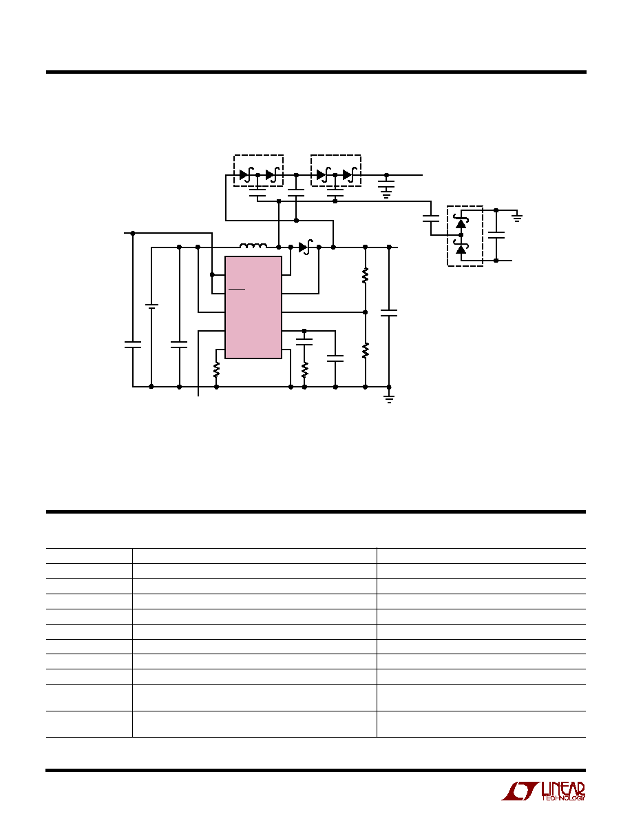
LTC3423
D1
V
DD
SHDN
V
IN
MODE/SYNC
R
t
SW
V
OUT
FB
V
C
GND
4
7
8
9
5
C4
470pF
C2
10
µ
F
RC
82k
R
t
30.1k
f
OSC
= 1MHz
R1
110k
R2
249k
L1
2.2
µ
H
C3
44
µ
F
(2
◊
22
µ
F)
C1: TAIYO YUDEN JMK212BJ225MG
C2: TAIYO YUDEN JMK212BJ106MM
C3: TAIYO YUDEN JMK325BJ226MM
D1: ON SEMICONDUCTOR MBRM120T3
D2 TO D7: ZETEX FMND7000 DUAL DIODE
L1: SUMIDA CD43-2R2M
V
DD
= 2.7V TO 5.5V
V
IN
= 0.9V TO 1.5V
0 = FIXED FREQ
1 = Burst Mode OPERATION
C5
4.7pF
3423/24 TA05
V
OUT
1.8V
700mA
1
CELL
V
DD
IN
+
≠
C1
2.2
µ
F
D2
D3
0.1
µ
F
0.1
µ
F
0.1
µ
F
4.7
µ
F
0.1
µ
F
4.7
µ
F
≠1.1V
1mA
D6
3.6V
2mA
D4
D5
D7
U
TYPICAL APPLICATIO
Triple Output Converter