LTC3721-1
1
sn37211 37211fs
APPLICATIO S
U
FEATURES
TYPICAL APPLICATIO
U
DESCRIPTIO
U
The LTC
Æ
3721-1 push-pull PWM controller provides all of
the control and protection functions necessary for com-
pact and highly efficient, isolated power converters. High
integration minimizes external component count, while
preserving design flexibility.
The robust push-pull output stages switch at half the
oscillator frequency. Dead-time is independently pro-
grammed with an external resistor. A UVLO program input
provides precise system turn-on and turn off voltages. The
LTC3721-1 features peak current mode control with pro-
grammable slope compensation and leading edge
blanking.
The LTC3721-1 features extremely low operating and
start-up currents and reliable short-circuit and
overtemperature protection. The LTC3721-1 is offered in
16-pin SSOP and (4mm ◊ 4mm) QFN packages.
Telecommunications, Infrastructure Power Systems
Distributed Power Architectures
Server Power Supplies
High Density Power Modules
, LTC and LT are registered trademarks of Linear Technology Corporation.
High Efficiency Push-Pull PWM
1.5A Sink, 1A Source Output Drivers
Adjustable Push-Pull Dead-Time
Adjustable System Undervoltage Lockout and
Hysteresis
Adjustable Leading Edge Blanking
Low Start-Up and Quiescent Currents
Current Mode Operation
Single Resistor Slope Compensation
V
CC
UVLO and 25mA Shunt Regulator
Programmable Fixed Frequency Operation to 1MHz
Soft-Start, Cycle-by-Cycle Current Limiting and
Hiccup Mode Short-Circuit Protection
5V, 15mA Low Dropout Regulator
16-Pin SSOP and (4mm ◊ 4mm) QFN Packages
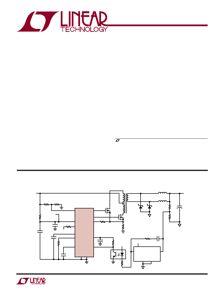
Push-Pull PWM Controller
R
CS
V
OUT
V
OUT
V
+
V
OUT
R
TOP
GND-F
LT1431
GND-S
COLL
R
REF
COMP
R
MID
37211 TA01
V
IN
FROM
AUXILIARY
WINDING
V
REF
+
DRVA
DRVB
CS
V
CC
DPRG
LTC3721-1
V
REF
COMP
UVLO
C
T
R
LEB
SS
FB
GND
Isolated Push-Pull Converter

LTC3721-1
2
sn37211 37211fs
V
CC
to GND (Low Impedance Source) .......≠ 0.3V to 10V
(Chip Self-Regulates at 10.3V)
UVLO to GND ............................................. ≠ 0.3V to V
CC
All Other Pins to GND
(Low Impedance Source) .........................≠ 0.3V to 5.5V
V
CC
(Current Fed) ................................................. 40mA
ORDER PART
NUMBER
GN PART
MARKING
T
JMAX
= 125∞C,
JA
= 100∞C/W
Consult LTC Marketing for parts specified with wider operating temperature ranges.
37211
LTC3721EGN-1
ABSOLUTE AXI U
RATI GS
W
W
W
U
PACKAGE/ORDER I FOR ATIO
U
U
W
(Note 1)
ELECTRICAL CHARACTERISTICS
The
denotes the specifications which apply over the full operating
temperature range, otherwise specifications are at T
A
= 25∞C. V
CC
= 9.5V unless otherwise noted.
V
REF
Output Current ............................... Self-Regulated
Operating Temperature (Notes 5,6)
LTC3721-1 ......................................... ≠ 40∞C to 85∞C
Storage Temperature Range ................. ≠ 65∞C to 125∞C
Lead Temperature (GN Package only)
(Soldering, 10sec) ............................................ 300∞C
ORDER PART
NUMBER
UF PART
MARKING
37211
LTC3721EUF-1
T
JMAX
= 125∞C,
JA
= 100∞C/W
EXPOSED PAD IS GND
(PIN17) MUST BE SOLDERED TO PCB
1
2
3
4
5
6
7
8
TOP VIEW
GN PACKAGE
16-LEAD PLASTIC SSOP
16
15
14
13
12
11
10
9
V
REF
NC
NC
DRVB
V
CC
DRVA
GND
C
T
NC
UVLO
SS
FB
R
LEB
COMP
CS
DPRG
SYMBOL
PARAMETER
CONDITIONS
MIN
TYP
MAX
UNITS
Input Supply
V
CCUV
V
CC
Undervoltage Lockout
Measured on V
CC
10.25
10.7
V
V
CCHY
V
CC
UVLO Hysteresis
Measured on V
CC
3.8
4.2
V
I
CCST
Start-Up Current
V
CC
= V
UVLO
≠ 0.3V
145
230
µA
I
CCRN
Operating Current
No Load on Outputs
3
6
mA
V
SHUNT
Shunt Regulator Voltage
Current into V
CC
= 10mA
10.3
10.8
V
R
SHUNT
Shunt Resistance
Current into V
CC
= 10mA to 17mA
1.4
3.5
SUVLO
System UVLO Threshold
Measured on UVLO Pin, 10mA into V
CC
4.8
5.0
5.2
V
SHYST
System UVLO Hysteresis Current
Current Flows Out of UVLO Pin, 10mA into V
CC
8.5
10
11.5
µA
16
17
15 14 13
5
6
7
8
TOP VIEW
UF PACKAGE
16-LEAD (4mm ◊ 4mm) PLASTIC QFN
9
10
11
12
4
3
2
1
DRVB
V
CC
DRVA
PGND
FB
R
LEB
COMP
CS
NC
V
REF
UVLO
SS
SGND
C
T
NC
DPRG

LTC3721-1
3
sn37211 37211fs
ELECTRICAL CHARACTERISTICS
The
denotes the specifications which apply over the full operating
temperature range, otherwise specifications are at T
A
= 25∞C. V
CC
= 9.5V unless otherwise noted.
SYMBOL
PARAMETER
CONDITIONS
MIN
TYP
MAX
UNITS
Pulse Width Modulator
ROS
Ramp Offset Voltage
Measured on COMP, CS = 0V
0.65
V
I
RMP
Ramp Discharge Current
CS = 1V, COMP = 0V, C
T
= 4V
50
mA
I
SLP
Slope Compensation Current
Measured on CS, C
T
= 1V
30
µA
C
T
= 2.25V
68
µA
DCMAX
Maximum Duty Cycle
COMP = 4.5V
47
48.2
50
%
DCMIN
Minimum Duty Cycle
COMP = 0V
0
%
DTADJ
Dead-Time
130
ns
Oscillator
OSCI
Initial Accuracy
T
A
= 25∞C, C
T
= 270pF
220
250
280
kHz
OSCT
V
CC
Variation
V
CC
= 6.5V to 9.5V
≠3
3
%
OSCV
C
T
Ramp Amplitude
Measured on C
T
2.35
V
Error Amplifier
V
FB
FB Input Voltage
COMP = 2.5V, (Note 3)
1.172
1.2
1.22
V
FB
I
FB Input Range
Measured on FB, (Note 4)
≠ 0.3
2.5
V
AVOL
Open-Loop Gain
COMP = 1V to 3V, (Note 3)
70
90
dB
I
IB
Input Bias Current
COMP = 2.5V, (Note 3)
5
50
nA
V
OH
Output High
Load on COMP = ≠100µA
4.7
4.92
V
V
OL
Output Low
Load on COMP = 100µA
0.27
0.5
V
I
SOURCE
Output Source Current
COMP = 2.5V
400
700
µA
I
SINK
Output Sink Current
COMP = 2.5V
2
5
mA
Reference
V
REF
Initial Accuracy
T
A
= 25∞C, Measured on V
REF
4.925
5.00
5.075
V
REFLD
Load Regulation
Load on V
REF
= 100µA to 5mA
2
15
mV
REFLN
Line Regulation
V
CC
= 6.5V to 9.5V
1
10
mV
REFTV
Total Variation
Line, Load and Temperature
4.900
5.000
5.100
V
REFSC
Short-Circuit Current
V
REF
Shorted to GND
18
30
45
mA
Push-Pull Outputs
DRVH(x)
Output High Voltage
I
OUT(x)
= ≠100mA
9.2
V
DRVL(x)
Output Low Voltage
I
OUT(x)
= 100mA
0.17
V
RDH(x)
Pull-Up Resistance
I
OUT(x)
= ≠10mA to ≠100mA
2.9
RDL(x)
Pull-Down Resistance
I
OUT(x)
= ≠10mA to ≠100mA
1.7
TDR(x)
Rise-Time
C
OUT(x)
= 1nF
10
ns
TDF(x)
Fall-Time
C
OUT(x)
= 1nF
10
ns
Current Limit and Shutdown
CLPP
Pulse by Pulse Current Limit Threshold
Measured on CS
280
300
320
mV
CLSD
Shutdown Current Limit Threshold
Measured on CS
475
600
725
mV
CLDEL
Current Limit Delay to Output
100mV Overdrive on CS, (Note 2)
80
ns
SSI
Soft-Start Current
SS = 2.5V
10
13
16
µA

LTC3721-1
4
sn37211 37211fs
SSR
Soft-Start Reset Threshold
Measured on SS
0.7
0.4
0.1
V
FLT
Fault Reset Threshold
Measured on SS
4.5
4.2
3.5
V
SYMBOL
PARAMETER
CONDITIONS
MIN
TYP
MAX
UNITS
ELECTRICAL CHARACTERISTICS
The
denotes the specifications which apply over the full operating
temperature range, otherwise specifications are at T
A
= 25∞C. V
CC
= 9.5V unless otherwise noted.
Note 1: Absolute Maximum Ratings are those values beyond which the life
of a device may be impaired.
Note 2: Includes leading edge blanking delay, R
LEB
= 20k, not tested in
production.
Note 3: FB is driven by a servo loop amplifier to control V
COMP
for these
tests.
Note 4: Set FB to ≠0.3V, 2.5V and insure that COMP does not phase invert.
Note 5: The LTC3721≠1 is guaranteed to meet performance specifications
from 0∞C to 85∞C. Specifications over the ≠40∞C to 85∞C operating
temperature range are assured by design, characterization and correlation
with statistical process controls.
Note 6: This IC includes overtemperature protection that is intended to
protect the device during momentary overload conditions. Junction
temperature will exceed 125∞C when overtemperature protection is active.
Continuous operation above the specified maximum operating junction
temperature may impair device reliability.
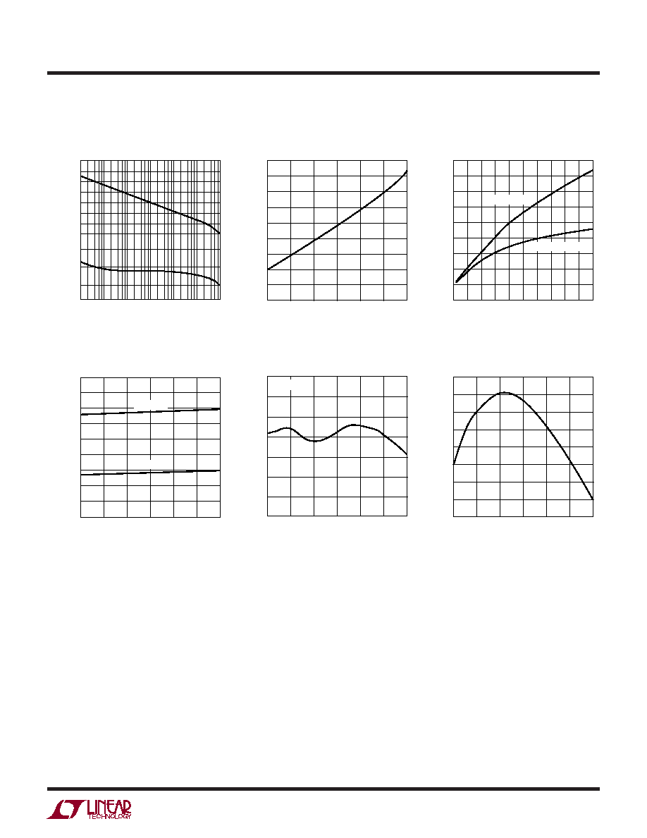
V
CC
(V)
0
I
CC
(
µ
A)
100
150
8
372311 G01
50
0
2
4
6
10
200
Start-Up I
CC
vs V
CC
V
CC
vs I
SHUNT
Oscillator Frequency vs
Temperature
TYPICAL PERFOR A CE CHARACTERISTICS
U
W
I
SHUNT
(mA)
0
V
CC
(V) 10.00
10.25
40
372311 G02
9.75
9.50
10
20
30
50
10.50
TEMPERATURE (∞C)
FREQUENCY (kHz)
240
250
80
372311 G03
230
220
≠ 40
≠ 60
≠ 20
20
0
40
60
100
260
C
T
= 270pF
(T
A
= 25∞C unless otherwise noted)
Leading Edge Blanking Time
vs R
LEB
V
REF
vs I
REF
V
REF
vs Temperature
R
LEB
(k)
0
BLANK TIME (ns)
350
300
250
200
150
100
50
0
372311 G04
40
100
20
10
30
50
70
90
60
80
I
REF
(mA)
0
V
REF
(V)
5.05
5.00
4.95
4.90
4.85
4.80
15
25
40
372311 G05
5
10
20
30
35
T
J
= 25∞C
T
J
= 85∞C
T
J
= ≠40∞C
TEMPERATURE (∞C)
V
REF
(V)
4.99
5.00
80
372311 G06
4.98
4.97
≠ 40
≠ 60
≠ 20
20
0
40
60
100
5.01
LTC3721-1
5
sn37211 37211fs
FREQUENCY (Hz)
GAIN (dB)
PHASE (DEG)
≠180
1M
372311 G07
≠270
≠360
10
1k
100
10k
100k
10M
100
80
60
40
20
0
TEMPERATURE (∞C)
≠55
I
CC
(
µ
A)
190
180
170
160
150
140
130
120
110
100
372311 G08
≠25
5
35
95
125
65
R
DPRG
(k)
0
50
DELAY (ns)
100
150
200
75
125
175
225
275
50 100 150 200
372311 G09
250
500
450
400
350
300
250
NO 200k PREBIAS
200k PREBIAS
TEMPERATURE (∞C)
≠55
CURRENT (
µ
A)
90
80
70
60
50
40
30
20
10
0
372311 G10
≠25
5
35
95
125
65
C
T
= 1V
C
T
= 2.25V
TEMPERATURE (∞C)
≠55
10.5
10.4
10.3
10.2
10.1
10.0
9.9
9.8
372311 G11
≠25
5
35
95
125
65
SHUNT VOLTAGE (V)
I
CC
= 10mA
Error Amplifier Gain/Phase
Start-Up I
CC
vs Temperature
TYPICAL PERFOR A CE CHARACTERISTICS
U
W
Deadtime vs R
DPRG
(T
A
= 25∞C unless otherwise noted)
Slope Current vs Temperature
V
CC
Shunt Voltage vs
Temperature
FB Input Voltage vs Temperature
TEMPERATURE (∞C)
≠55
FB VOLTAGE (V)
1.205
1.204
1.203
1.202
1.201
1.200
1.199
1.198
1.197
372311 G12
≠25
5
35
95
125
65