 | –≠–ª–µ–∫—Ç—Ä–æ–Ω–Ω—ã–π –∫–æ–º–ø–æ–Ω–µ–Ω—Ç: MP02HB175 | –°–∫–∞—á–∞—Ç—å:  PDF PDF  ZIP ZIP |
1/7
www.dynexsemi.com
MP02XX175 Series
MP02XX175 Series
Dual Diode Modules
Replaces January 2000 version, DS5101-4.0
DS5101-5.0 July 2002
FEATURES
s
Dual Device Module
s
Electrically Isolated Package
s
Pressure Contact Construction
s
International Standard Footprint
s
Alumina (non-toxic) Isolation Medium
APPLICATIONS
s
Rectifier Bridges
s
DC Power Supplies
s
Plating Rectifiers
s
Traction Systems
VOLTAGE RATINGS
ORDERING INFORMATION
Order As:
MP02HB175-20 or MP02HB175-18 or MP02HB175-16 or
MP02HB175-14 or MP02HB175-12 or MP02HB175-10 or
MP02HB175-08
MP02G175-20 or MP02G175-18 or MP02G175-16 or
MP02G175-14 or MP02G175-12 or MP02G175-10 or
MP02G175-08
MP02GN175-20 or MP02GN175-18 or MP02GN175-16 or
MP02GN175-14 or MP02GN175-12 or MP02GN175-10 or
MP02GN175-08
Note: When ordering, please use the complete part number.
KEY PARAMETERS
V
RRM
2000V
I
FSM
5625A
I
F(AV)(per arm)
170A
V
isol
3000V
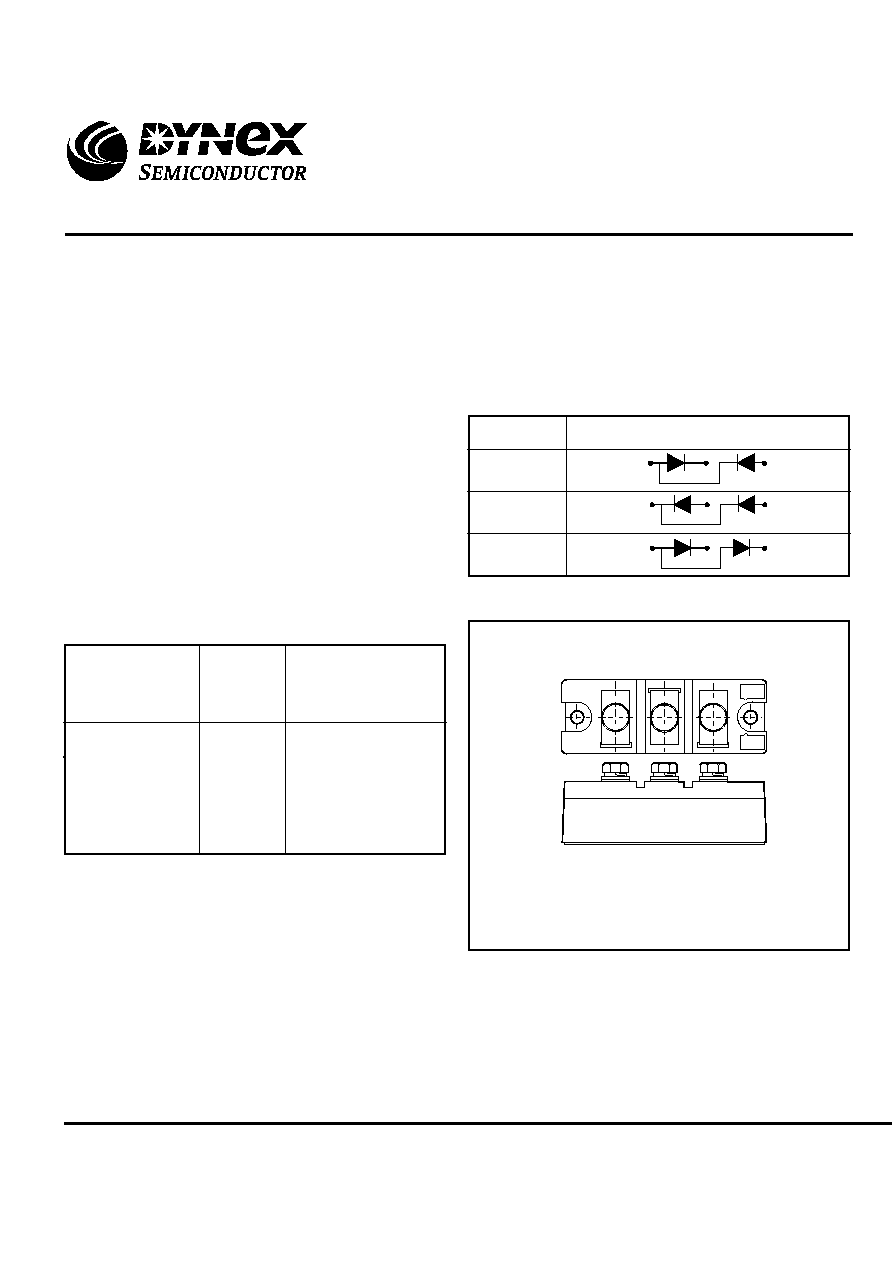
Code
Circuit
HB
G
GN
1
2
3
1
2
3
1
2
3
Fig.1 Circuit diagrams
Fig. 2 Electrical connections - (not to scale)
Module type code: MP02.
For further information see Package Details.
Lower voltage grades available.
Repetitive
Peak
Voltages
V
DRM
V
RRM
Type
Number
2000
1800
1600
1400
1200
1000
800
MP02XX175-20
MP02XX175-18
MP02XX175-16
MP02XX175-14
MP02XX175-12
MP02XX175-10
MP02XX175-08
T
vj
= 150
o
C
I
DRM
= I
RRM
= 30mA
V
DSM
& V
RSM
=
V
DRM
& V
RRM
+ 100V
respectively
Conditions
2/7
www.dynexsemi.com
MP02XX175 Series
ABSOLUTE MAXIMUM RATINGS - PER ARM
Stresses above those listed under 'Absolute Maximum Ratings' may cause permanent damage to the device. In extreme
conditions, as with all semiconductors, this may include potentially hazardous rupture of the package. Appropriate safety
precautions should always be followed. Exposure to Absolute Maximum Ratings may affect device reliability.
Test Conditions
Half wave resistive load
T
case
= 75∞C
T
case
= 85∞C
T
case
= 75∞C
10ms half sine, T
j
= 150∞C
V
R
= 0
10ms half sine, T
j
= 150∞C
V
R
= 50% V
DRM
Commoned terminals to base plate.
AC RMS, 1 min, 50Hz
Symbol
I
F(AV)
I
F(RMS)
I
FSM
I
2
t
I
FSM
I
2
t
V
isol
Units
A
A
A
kA
A
2
s
kA
A
2
s
V
Max.
170
152
267
5.625
158 x 10
3
4.5
100 x 10
3
3000
Parameter
Mean forward current
RMS value
Surge (non-repetitive) forward current
I
2
t for fusing
Surge (non-repetitive) forward current
I
2
t for fusing
Isolation voltage
Test Conditions
dc
Half wave
3 Phase
Mounting torque = 6Nm
with mounting compound
Reverse (blocking)
-
Mounting - M6
Electrical connections - M6
-
Parameter
Thermal resistance - junction to case
(per thyristor or diode)
Thermal resistance - case to heatsink
(per thyristor or diode)
Virtual junction temperature
Storage temperature range
Screw torque
Weight (nominal)
THERMAL AND MECHANICAL RATINGS
Symbol
R
th(j-c)
R
th(c-hs)
T
vj
T
stg
-
-
Units
∞C/kW
∞C/kW
∞C/kW
∞C/kW
∞C
∞C
Nm (lb.ins)
Nm (lb.ins)
g
Max.
0.37
0.38
0.39
0.07
150
150
6 (55)
5 (44)
350
Min.
-
-
-
-
-
≠40
-
-
-
3/7
www.dynexsemi.com
MP02XX175 Series
Units
mA
V
m
Test Conditions
At V
RRM
, T
j
= 150∞C
At T
vj
= 150∞C. See note 1
At T
vj
= 150∞C. See note 1
Parameter
Peak reverse current
Threshold voltage
Forward slope resistance
DYNAMIC CHARACTERISTICS
Symbol
I
RRM
V
TO
r
T
Max.
30
0.81
0.84
Min.
-
-
-
Note 1: The data given in this datasheet with regard to forward voltage drop is for calculation of the power dissipation in the
semiconductor elements only. Forward voltage drops measured at the power terminals of the module will be in excess of these
figures due to the impedance of the busbar from the terminal to the semiconductor.
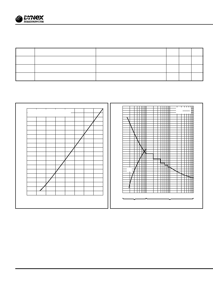
Fig. 3 Maximum (limit) forward characteristics
Fig. 4 Surge (non-repetitive) forward current vs time
(With 50% V
RRM
at T
case
= 150∞C)
0.5
1.0
1.5
2.0
2.5
Instantaneous forward voltage, V
F
- (V)
2000
1500
1000
500
0
Instantaneous forward current, I
F
- (A)
Measured under pulse conditions
T
j
= 150∞C
0
2.0
1.0
3.0
4.0
5.0
6.0
Peak half sine wave forward current - (kA)
1
10
1
2 3
5
50
10
20 30
ms
cycles at 50Hz
Duration
5
6
7
8
9
10
I
2
t value - (A
2
s x 10
4
)
I
2
t
7.0
8.0
9.0
10.0
I
2
t = Œ
2
x t
2
4/7
www.dynexsemi.com
MP02XX175 Series
Fig. 6 On-state power loss per arm vs forward current at
various conduction angles, 50/60Hz
Fig. 5 Transient thermal impedance - dc (per diode)
100
10
1.0
0.1
0.01
0.001
Time - (s)
0.4
0.3
0.2
0.1
0
Thermal impedance - (
∞
C/W)
d.c.
Fig. 7 Maximum permissible case temperature vs forward
current per arm at various conduction angles, 50/60Hz
0
50
100
150
200
250
300
Mean forward current, I
F(AV)
- (A)
120
100
80
60
40
20
0
Maximum permissible case temperature - (
∞
C)
d.c.
180
∞
120
∞
60
∞
140
160
180
∞
Rectangular
Sine
0
50
100
150
200
250
300
Mean forward current, I
T(AV)
- (A)
300
250
200
150
100
50
0
On-state power loss per device - (W)
d.c.
120∞
180∞
60∞
180∞
Rectangular
Sine
5/7
www.dynexsemi.com
MP02XX175 Series
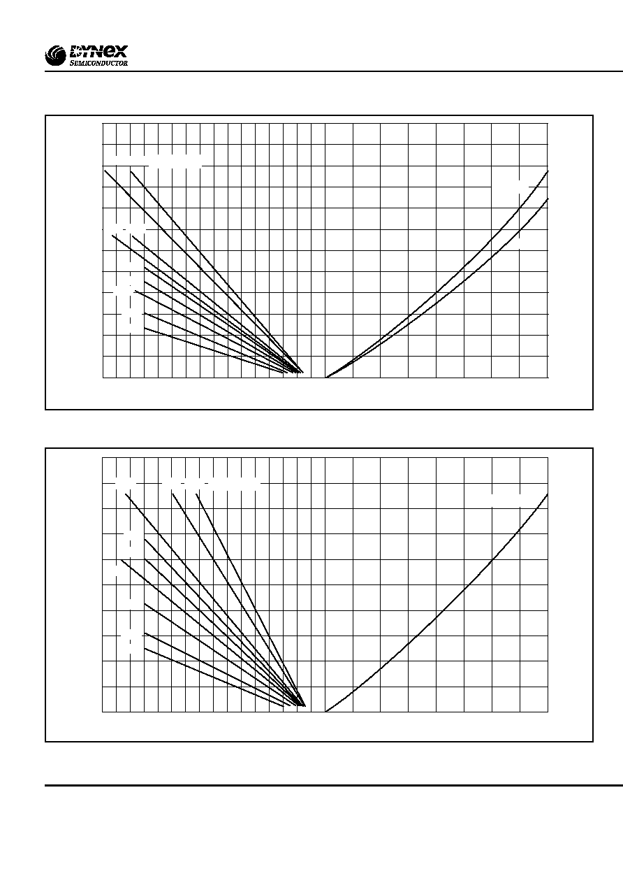
Fig. 8 50/60Hz single phase bridge dc output current vs power loss and maximum permissible ambient temperature for
various values of heatsink thermal resistance.
(Note: R
th(hs-a)
values given above are true heatsink thermal resistances to ambient and already account for R
th(c-hs)
module contact thermal).
Fig. 7 50/60Hz 3- phase bridge dc output current vs power loss and maximum permissible ambient temperature for various
values of heatsink thermal resistance.
(Note: R
th(hs-a)
values given above are true heatsink thermal resistances to ambient and already account for R
th(c-hs)
module contact thermal).
40
80
120
0
100
200
300
1200
1000
800
600
400
200
0
Total power - (W)
140
100
60
Maximum ambient temperature - (∞C)
D.C. output current - (A)
400
R - Load
L - Load
R
th(hs-a)
∞C/W
0.02
0.04
0.08
0.10
0.12
0.15
0.20
0.40
0.30
0
20
40
80
120
0
100
200
300
1000
800
600
400
200
0
Total power - (W)
140
100
60
Maximum ambient temperature - (∞C)
D.C. output current - (A)
400
R & L - Load
R
th(hs-a)
∞C/W
0.02
0.04
0.08
0.10
0.12
0.15
0.20
0.40
0.30
0
20