MP02TT200
1/9
www.dynexsemi.com
FEATURES
s
Dual Device Module
s
Electrically Isolated Package
s
Pressure Contact Construction
s
International Standard Footprint
s
Alumina (Non Toxic) Isolation Medium
s
Integral Water Cooled Heatsink
APPLICATIONS
s
Motor Control
s
Controlled Rectifier Bridges
s
Heater Control
s
AC Phase Control
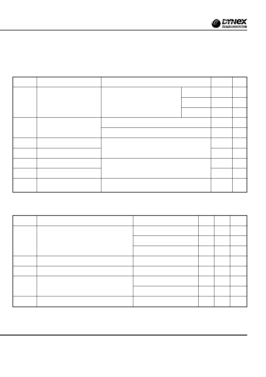
VOLTAGE RATINGS
ORDERING INFORMATION
Order As:
MP02TT200-XX-W12
1/4 - 18 NPT connection
MP02TT200-XX-W13
1/4 BSP connection
XX shown in the part number about represents V
DRM
/100
selection required, e.g. MP02TT200-14-W12
Note: When ordering, please use the whole part number.
Auxiliary gate and cathode leads can be ordered separately.
KEY PARAMETERS
V
DRM
1600V
I
T(AV)
200A
I
TSM(per arm)
6800A
I
T(RMS)
318A
V
isol
3000V
MP02TT200
Dual Thyristor Water Cooled Module
Advance Information
DS5434-1.1 April 2001
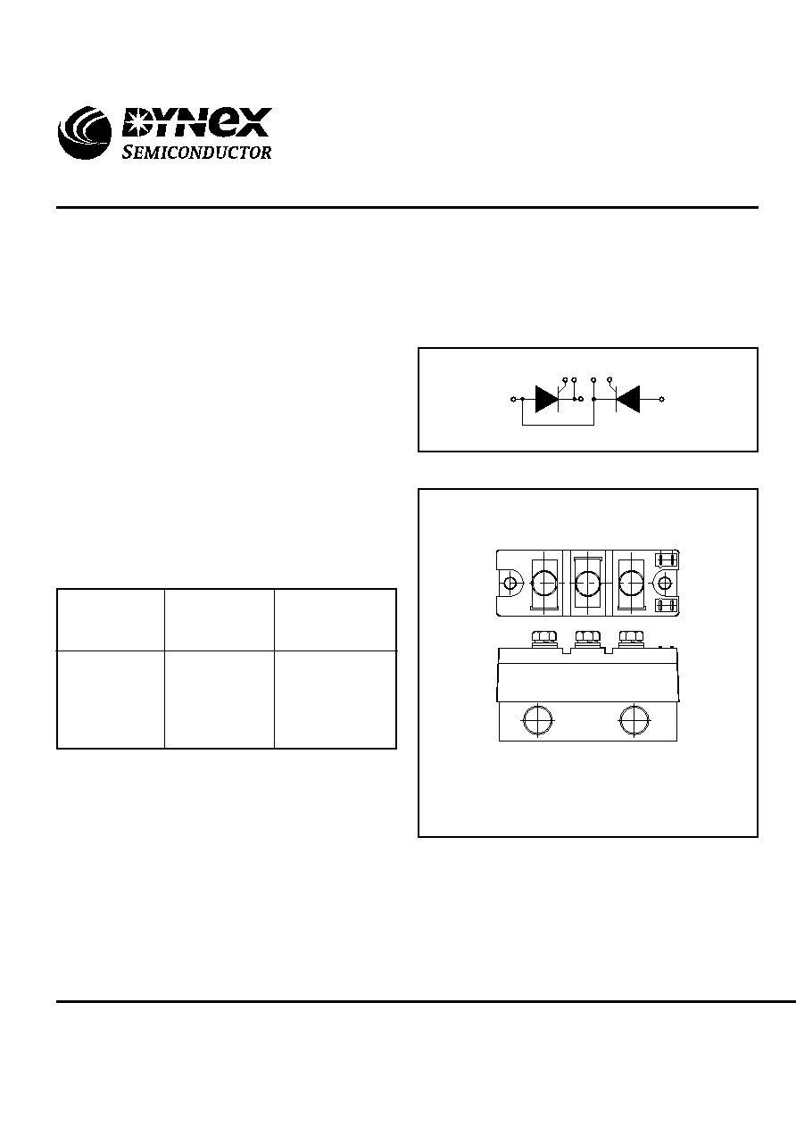
Fig. 1 Circuit diagram
Fig. 2 Electrical connections - (not to scale)
Outline type code: MP02 W12/W13
(See package details for further information)
1600
1500
1400
1300
1200
MP02TT200-16
MP02TT200-15
MP02TT200-14
MP02TT200-13
MP02TT200-12
Conditions
T
vj
= 0∞ to 125∞C,
I
DRM
= I
RRM
= 30mA
V
DSM
= V
RSM
=
V
DRM
= V
RRM
+ 100V
respectively
Lower voltage grades available
Type Number
Repetitive Peak
Voltages
V
DRM
V
RRM
V
G
1
K
1
K
2
G
2
1
2
3
K1 G1
K2 G2
1
2
3
MP02TT200
2/9
www.dynexsemi.com
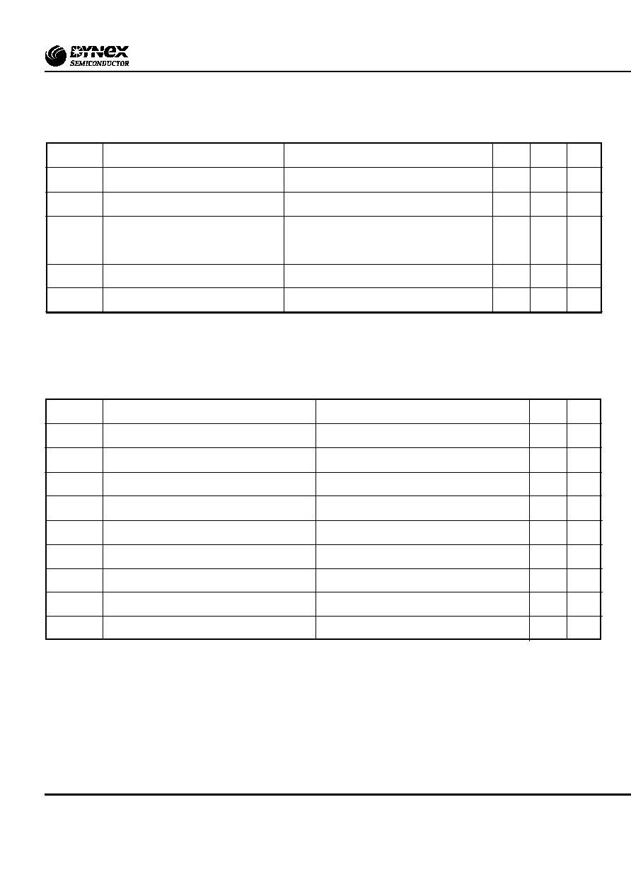
Test Conditions
Half wave resistive load,
T
water (in)
= 25∞C
4.5 Ltr/min
T
water (in)
= 40∞C
T
water (in)
= 50∞C
T
water (in)
= 25∞C @ 4.5 Ltr/min
T
water (in)
= 40∞C @ 4.5 Ltr/min
10ms half sine, T
j
= 125∞C
V
R
= 0
10ms half sine, T
j
= 125∞C
V
R
= 50% V
DRM
Commoned terminals to base plate.
AC RMS, 1 min, 50Hz
Symbol
I
T(AV)
I
T(RMS
I
TSM
I
2
t
I
TSM
I
2
t
V
isol
Units
A
A
A
A
A
kA
A
2
s
kA
A
2
s
V
Max.
230
200
180
360
318
6.8
0.231 x 10
6
5.5
0.15 x 10
6
3000
Test Conditions
dc, 4.5 Ltr/min
Half wave, 4.5 Ltr/min
3 Phase, 4.5 Ltr/min
Reverse (blocking)
-
Mounting - M6
Electrical connections - M6
-
Parameter
Thermal resistance - junction to water
(per thyristor)
Virtual junction temperature
Storage temperature range
Screw torque
Weight (nominal)
THERMAL AND MECHANICAL RATINGS
ABSOLUTE MAXIMUM RATINGS - PER ARM
Stresses above those listed under 'Absolute Maximum Ratings' may cause permanent damage to the device. In extreme
conditions, as with all semiconductors, this may include potentially hazardous rupture of the package. Appropriate safety
precautions should always be followed. Exposure to Absolute Maximum Ratings may affect device reliability.
Parameter
Mean on-state current
RMS value
Surge (non-repetitive) on-current
I
2
t for fusing
Surge (non-repetitive) on-current
I
2
t for fusing
Isolation voltage
Symbol
R
th(j-w)
T
vj
T
stg
-
-
Units
∞C/kW
∞C/kW
∞C/kW
∞C
∞C
Nm (lb.ins)
Nm (lb.ins)
g
Max.
0.3
0.32
0.33
125
125
-
5 (44)
1200
Min.
-
-
-
-
≠40
5 (44)
-
-
MP02TT200
3/9
www.dynexsemi.com
Units
mA
V/
µ
s
A/
µ
s
V
m
Test Conditions
At V
RRM
/V
DRM
, T
j
= 125∞C
To 67% V
DRM
, T
j
= 125∞C
From 67% V
DRM
to 200A, gate source 10V, 5
t
r
= 0.5
µ
s, T
j
= 125∞C
At T
vj
= 125∞C
At T
vj
= 125∞C
Parameter
Peak reverse and off-state current
Linear rate of rise of off-state voltage
Rate of rise of on-state current
Threshold voltage
On-state slope resistance
DYNAMIC CHARACTERISTICS
Symbol
I
RRM
/I
DRM
dV/dt
dI/dt
V
T(TO)
r
T
Max.
30
1000
500
0.98
0.75
Min.
-
-
-
-
-
Parameter
Gate trigger voltage
Gate trigger current
Gate non-trigger voltage
Peak forward gate voltage
Peak forward gate voltage
Peak reverse gate voltage
Peak forward gate current
Peak gate power
Mean gate power
Test Conditions
V
DRM
= 5V, T
case
= 25
o
C
V
DRM
= 5V, T
case
= 25
o
C
At V
DRM
T
case
= 125
o
C
Anode positive with respect to cathode
Anode negative with respect to cathode
-
Anode positive with respect to cathode
See table fig. 5
-
Symbol
V
GT
I
GT
V
GD
V
FGM
V
FGN
V
RGM
I
FGM
P
GM
P
G(AV)
GATE TRIGGER CHARACTERISTICS AND RATINGS
Max.
3
150
0.25
30
0.25
5
10
100
5
Units
V
mA
V
V
V
V
A
W
W
Note 1: The data given in this datasheet with regard to forward voltage drop is for calculation of the power dissipation in the
semiconductor elements only. Forward voltage drops measured at the power terminals of the module will be in excess of these
figures due to the impedance of the busbar from the terminal to the semiconductor.
MP02TT200
4/9
www.dynexsemi.com
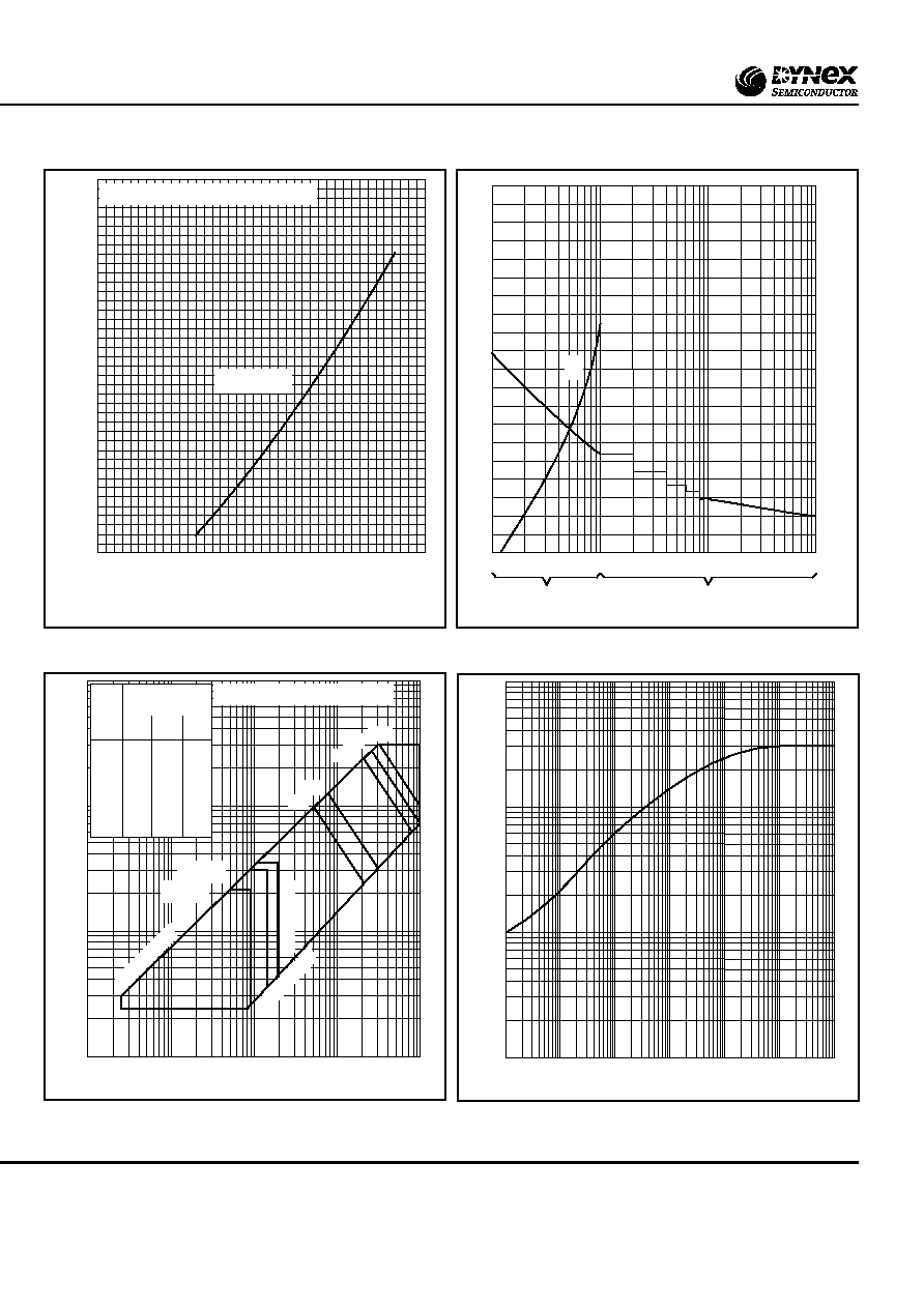
Fig. 3 Maximum (limit) on-state characteristics
1
10
1
2
3 4 5
50
0
5
10
15
Duration
60
100
140
Peak half sine wave on-state current - (kA)
ms
cycles at 50Hz
I
2
t value - A
2
s x 10
3
180
I
2
t
20
10
20 30
Fig. 6 Transient thermal impedance - dc
Fig. 4 Surge (non-repetitive) on-state current vs time
(with 50% V
RSM
at T
case
= 125∞C)
Fig. 5 Gate characteristics
0.5
1.0
2.0
Instantaneous on-state voltage, V
T
- (V)
0
500
1000
1500
2000
Instantaneous on-state current, I
T
- (A)
Measured under pulse conditions
T
j
= 125∞C
1.5
2.5
100
10
1.0
0.1
0.001
0.01
0.1
1.0
10
Gate trigger current, I
GT
- (A)
Gate trigger voltage, V
GT
- (V)
T
j
= 125∞C
T
j
= 25∞C
T
j
= -40
∞
C
Upper limit 99%
Lower li
mit 1%
V
FGM
V
GD
I
FGM
5W
10W
50W
75W
100W
Pulse
Width
µs
20
25
100
500
1ms
10ms
50
100
100
100
100
100
10
100
100
100
100
100
50
-
400
100
100
100
25
-
-
Pulse Frequency
Hz
Table gives pulse power P
GM
in watts
10
1
0.1
1000
100
0.01
0.001
Time - (s)
1.0
0.1
0.01
0.001
Thermal resistance (junction to water). R
th(j-w)
- (
þ
C/W)
MP02TT200
5/9
www.dynexsemi.com
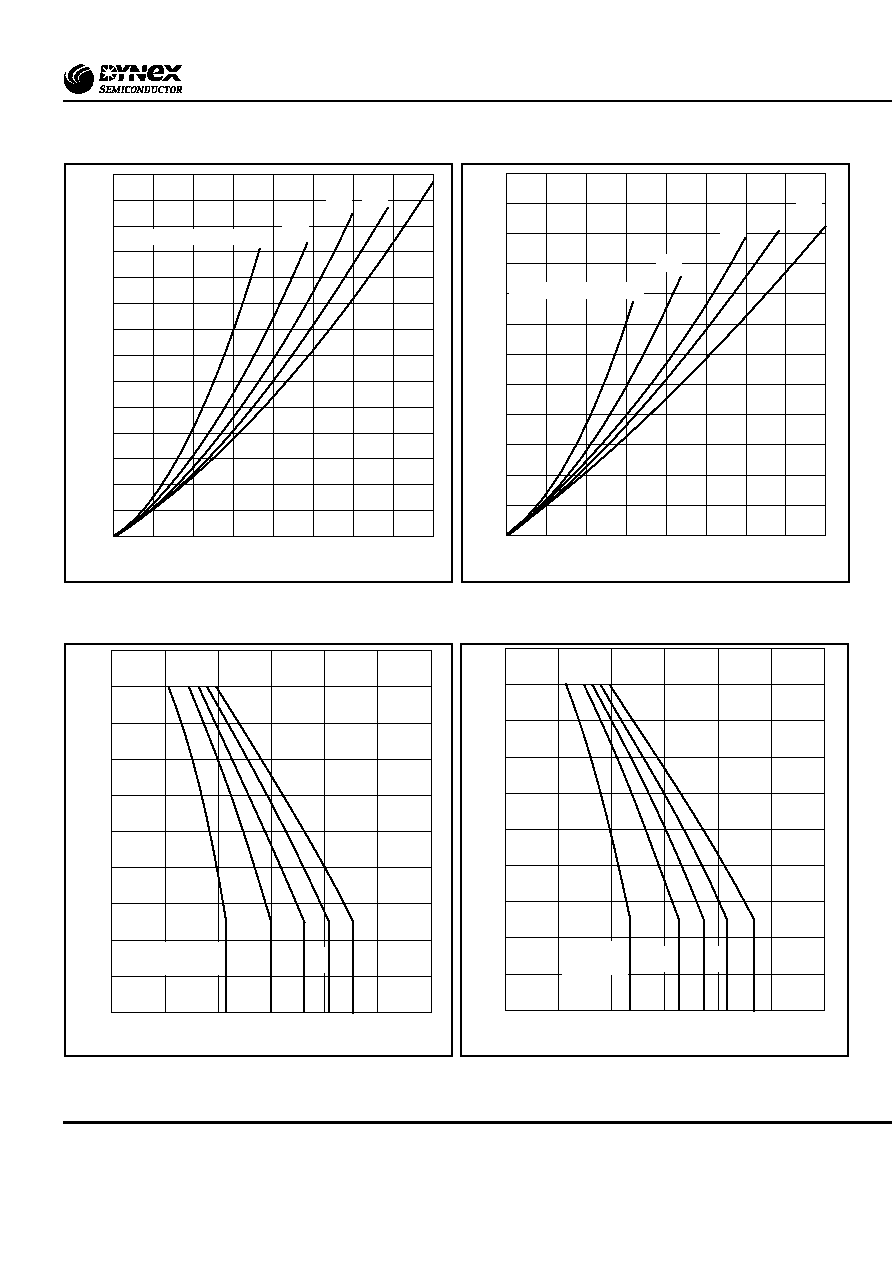
Fig. 7 On-state power loss per arm vs on-state current at
specified conduction angles, sine wave 50/60Hz
Fig. 8 On-state power loss per arm vs on-state current at
specified conduction angles, square wave 50/60Hz
Fig. 9 Maximum permissible water inlet temperature vs on-
state current at specified conduction angles,
sine wave 50/60Hz
Fig. 10 Maximum permissible water inlet temperature vs on-
state current at specified conduction angles,
square wave 50/60Hz
0
100
200
300
400
Mean on-state current, I
T(AV)
- (A)
0
200
400
500
700
On-state power loss per device - (W)
100
300
600
Conduction Angle 30∞
60∞
90∞
180∞
120∞
0
100
200
300
400
Mean on-state current, I
T(AV)
- (A)
0
200
400
500
On-state power loss per device - (W)
100
300
600
Conduction Angle 30∞
60∞
90∞
180∞
120∞
0
50
100
150
200
250
200
Mean on-state current, I
T(AV)
- (A)
0
20
40
60
Max. permissible water inlet temperature - (
∞
C @ 4.5 l/min)
10
30
50
70
90
80
100
60
∞
90
∞
180
∞
120
∞
Conduction
Angle 30∞
0
50
100
150
200
250
200
Mean on-state current, I
T(AV)
- (A)
0
20
40
60
Max. permissible water inlet temperature - (
∞
C @ 4.5 l/min)
10
30
50
70
90
80
100
60
∞
90
∞
180
∞
120
∞
Conduction
Angle 30∞