MP03XXX360H
1/8
www.dynexsemi.com
FEATURES
I
Dual Device Module
I
Electrically Isolated Package
I
Pressure Contact Construction
I
International Standard Footprint
I
Alumina (Non Toxic) Isolation Medium
APPLICATIONS
I
Motor Control
I
Controlled Rectifier Bridges
I
Heater Control
I
AC Phase Control
VOLTAGE RATINGS
ORDERING INFORMATION
Order As:
MP03HBT360-18 or MP03HBT360-16
MP03HBN360-18 or MP03HBN360-16
MP03HBP360-18 or MP03HBP360-16
Note: When ordering, please use the complete part number.
KEY PARAMETERS
V
DRM
1800V
I
T(AV)
355A
I
TSM(per arm)
8100A
V
isol
3000V
MP03XXX360H
Dual Thyristor, Thyristor/Diode Module
DS5560-1.0 July 2002
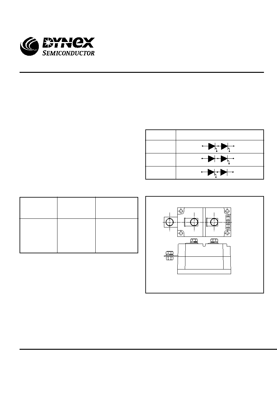
Fig. 2 Electrical connections - (not to scale)
Outline type code: MP03
1800
1600
MP03XXX360-18
MP03XXX360-16
Conditions
T
vj
= 0∞ to 130∞C,
I
DRM
= I
RRM
= 50mA
V
DSM
= V
RSM
=
V
DRM
= V
RRM
+ 100V
respectively
Lower voltage grades available.
Type Number
Repetitive Peak
Voltages
V
DRM
V
RRM
V
1
2
3
K
2
G
2
G
1
K
1
Code
Circuit
HBT
HBP
HBN
Fig.1 Circuit diagrams
MP03XXX360H
2/8
www.dynexsemi.com
Test Conditions
Half wave resistive load
T
case
= 75∞C
T
case
= 85∞C
T
heatsink
= 75∞C
T
heatsink
= 85∞C
T
case
= 75∞C
10ms half sine, T
j
= 130∞C
V
R
= 0
10ms half sine, T
j
= 130∞C
V
R
= 50% V
DRM
Commoned terminals to base plate.
AC RMS, 1 min, 50Hz
Symbol
I
T(AV)
I
T(RMS
I
TSM
I
2
t
I
TSM
I
2
t
V
isol
Units
A
A
A
A
A
kA
A
2
s
kA
A
2
s
V
Max.
355
312
276
242
560
8.1
330 x10
3
6.5
210 x10
3
3000
ABSOLUTE MAXIMUM RATINGS - PER ARM
Stresses above those listed under 'Absolute Maximum Ratings' may cause permanent damage to the device. In extreme
conditions, as with all semiconductors, this may include potentially hazardous rupture of the package. Appropriate safety
precautions should always be followed. Exposure to Absolute Maximum Ratings may affect device reliability.
Parameter
Mean on-state current
RMS value
Surge (non-repetitive) on-current
I
2
t for fusing
Surge (non-repetitive) on-current
I
2
t for fusing
Isolation voltage
Test Conditions
dc
Half wave
3 Phase
Mounting torque = 5Nm
with mounting compound
Reverse (blocking)
-
Mounting - M5
Electrical connections - M8
-
Parameter
Thermal resistance - junction to case
(per thyristor or diode)
Thermal resistance - case to heatsink
(per thyristor or diode)
Virtual junction temperature
Storage temperature range
Screw torque
Weight (nominal)
THERMAL AND MECHANICAL RATINGS
Symbol
R
th(j-c)
R
th(c-hs)
T
vj
T
stg
-
-
Units
∞C/kW
∞C/kW
∞C/kW
∞C/kW
∞C
∞C
Nm (lb.ins)
Nm (lb.ins)
g
Max.
0.105
0.115
0.12
0.05
135
135
5(44)
9(80)
950
Min.
-
-
-
-
-
≠40
-
-
-
MP03XXX360H
3/8
www.dynexsemi.com
Units
mA
V/
µs
A/
µs
V
m
Test Conditions
At V
RRM
/V
DRM
, T
j
= 130∞C
To 67% V
DRM
, T
j
= 130∞C
From 67% V
DRM
to 600A, gate source 10V, 5
t
r
= 0.5
µs, T
j
= 130∞C
At T
vj
= 135∞C. See note 1
At T
vj
= 135∞C. See note 1
Parameter
Peak reverse and off-state current
Linear rate of rise of off-state voltage
Rate of rise of on-state current
Threshold voltage
On-state slope resistance
DYNAMIC CHARACTERISTICS - THYRISTOR
Symbol
I
RRM
/I
DRM
dV/dt
dI/dt
V
T(TO)
r
T
Max.
50
1000
500
0.78
0.79
Min.
-
-
-
-
-
Parameter
Gate trigger voltage
Gate trigger current
Gate non-trigger voltage
Peak forward gate voltage
Peak forward gate voltage
Peak reverse gate voltage
Peak forward gate current
Peak gate power
Mean gate power
Test Conditions
V
DRM
= 5V, T
case
= 25
o
C
V
DRM
= 5V, T
case
= 25
o
C
At V
DRM
T
case
= 125
o
C
Anode positive with respect to cathode
Anode negative with respect to cathode
-
Anode positive with respect to cathode
See table fig. 5
-
Symbol
V
GT
I
GT
V
GD
V
FGM
V
FGN
V
RGM
I
FGM
P
GM
P
G(AV)
GATE TRIGGER CHARACTERISTICS AND RATINGS
Max.
3
150
0.25
30
0.25
5
10
100
5
Units
V
mA
V
V
V
V
A
W
W
Note 1: The data given in this datasheet with regard to forward voltage drop is for calculation of the power dissipation in the
semiconductor elements only. Forward voltage drops measured at the power terminals of the module will be in excess of these
figures due to the impedance of the busbar from the terminal to the semiconductor.
MP03XXX360H
4/8
www.dynexsemi.com
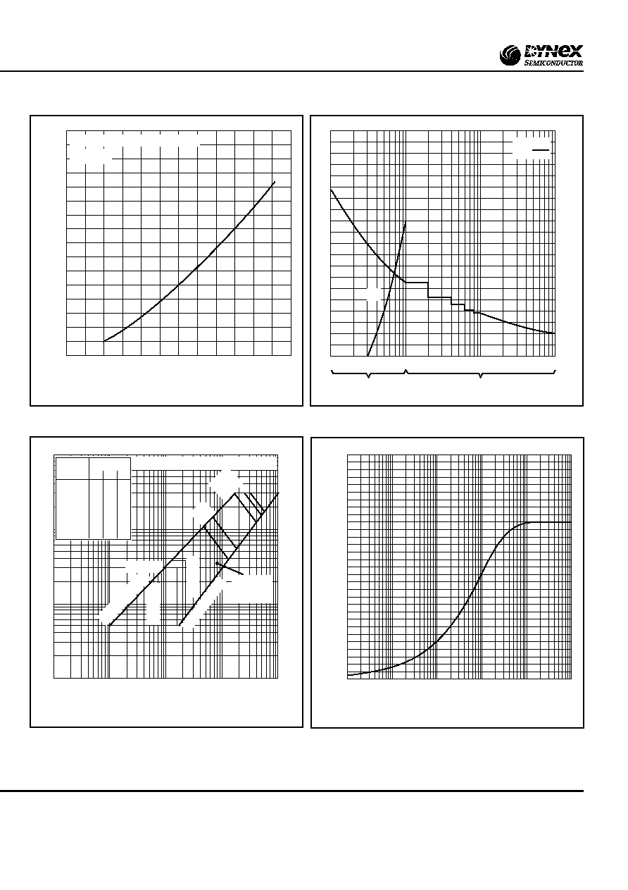
Fig. 6 Transient thermal impedance - dc
Fig. 3 Maximum (limit) on-state characteristics
Fig. 4 Surge (non-repetitive) on-state current vs time
(with 50% V
RSM
at T
case
= 130∞C)
Fig. 5 Gate characteristics
1600
1200
800
400
1400
1000
600
200
0
Instantaneous on-state current, I
T
- (A)
0.6
1.0
1.4
1.8
Instantaneous on-state voltage, V
T
- (V)
Measured under pulse conditions
T
j
= 135∞C
0.8
1.2
1.6
20
15
10
5
0
Peak half sine wave on-state current - (kA)
1
10
1
2
3 4 5
50
ms
Cycles at 50Hz
Duration
150
175
200
I
2
t value - (A
2
s x 10
3
)
I
2
t
I
2
t = Œ
2
x t
2
10
20 30
100
10
1
0.1
0.001
0.1
0.01
I
GD
0.1
10
I
FGM
V
FGM
Lower Limit 1%
Upper Limi
t 99%
T
j
=
≠
40
∞
C
T
j
= 25∞C
T
j
= 125
∞
C
Gate trigger voltage, V
GT
- (V)
Gate trigger current, I
GT
- (A)
100
W
75
W
50W
10
W
5W
Table gives pulse power P
GM
in Watts
Pulse width
µs
20
25
100
500
1ms
10ms
Frequency Hz
50
100
100
100
100
100
10
100
100
100
100
100
50
-
400
100
100
100
25
-
-
Region of
certain
triggering
100
10
1.0
0.1
0.01
0.001
Time - (s)
0.15
0
0.10
0.05
Thermal impedance, R
th(j-c)
- (
∞
C/W)
d.c.
MP03XXX360H
5/8
www.dynexsemi.com
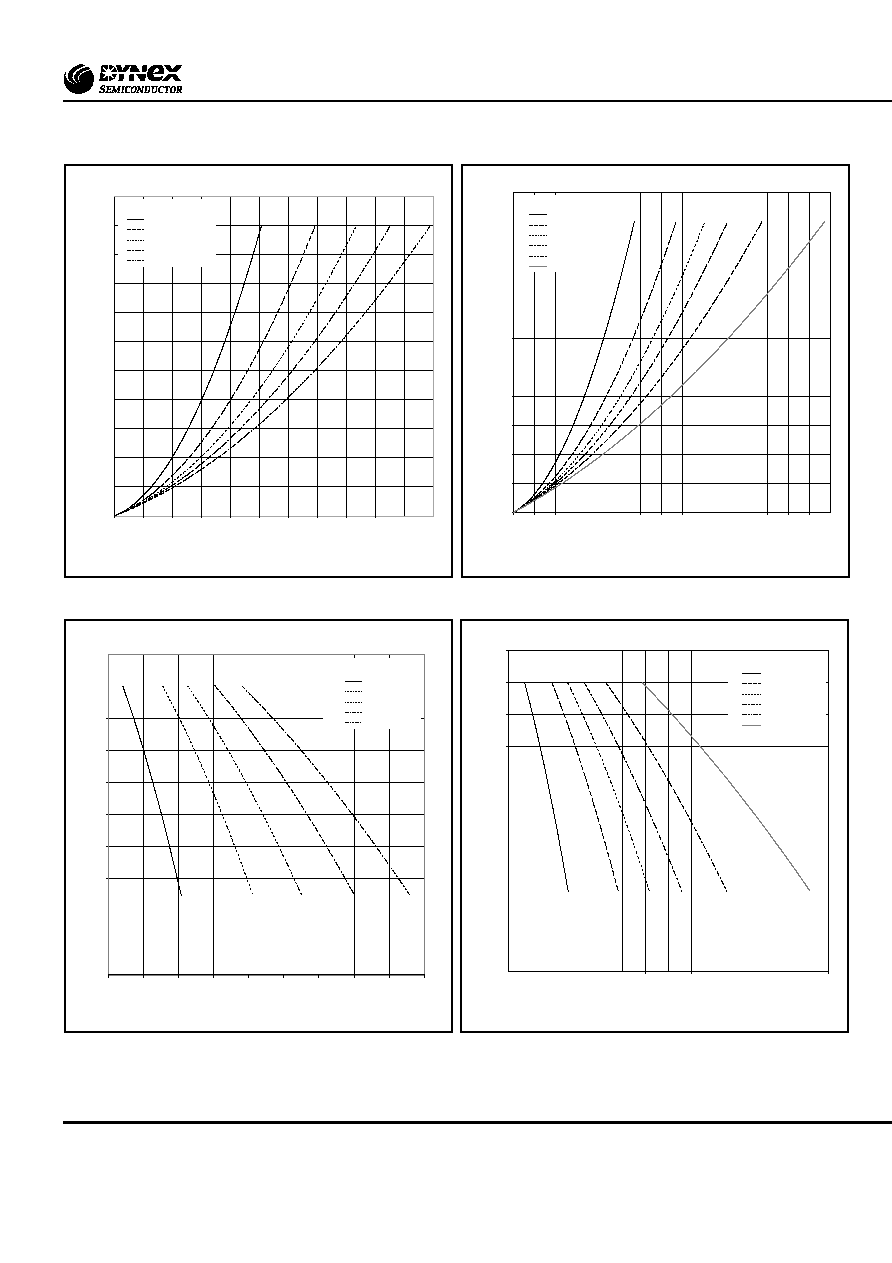
Fig. 7 On-state power loss per arm vs on-state current at
specified conduction angles, sine wave 50/60Hz
Fig. 8 On-state power loss per arm vs on-state current at
specified conduction angles, square wave 50/60Hz
Fig. 9 Maximum permissible case temperature vs
on-state current at specified conduction angles,
sine wave 50/60Hz
Fig. 10 Maximum permissible case temperature vs
on-state current at specified conduction angles,
square wave 50/60Hz
0
100
200
300
400
500
600
700
800
900
1000
1100
0
50 100 150 200 250 300 350 400 450 500 550
Sine wave current (Average, per arm)
Power dissipation (Watts, per arm)
30∞
60∞
90∞
120∞
180∞
Conduction angle
0
100
200
300
400
500
600
700
800
900
1000
1100
0
50
150
250
350
450
550
650
750
Square wave current (Average, per arm)
Power dissipation (Watts, per arm)
30∞
60∞
90∞
120∞
180∞
DC
Conduction angle
0
10
20
30
40
50
60
70
80
90
100
100
150
200
250
300
350
400
450
500
550
Sine wave current (Average, per arm) - (A)
Maximum permissble case temperature - (
∞
C)
30∞
60∞
90∞
120∞
180∞
Conduction angle
0
10
20
30
40
50
60
70
80
90
100
100
200
300
400
500
600
700
800
Square wave current (Average, per arm) - (A)
Maximum permissible case temperature - (
∞
C)
30∞
60∞
90∞
120∞
180∞
DC
Conduction angle