FEATURES
Direct Replacement for SILICONIX U/SST440 & U/SST441
HIGH CMRR
CMRR 85dB
LOW GATE LEAKAGE
I
GSS
1pA
ABSOLUTE MAXIMUM RATINGS
1
@ 25 įC (unless otherwise stated)
Maximum Temperatures
Storage Temperature
-65 to +150 įC
Operating Junction Temperature
-55 to +135 įC
Maximum Power Dissipation
Continuous Power Dissipation (Total)
500mW
Maximum Currents
Gate Current
50mA
Maximum Voltages
Gate to Drain
-25V
Gate to Source
-25V
Gate to Gate
Ī50V
MATCHING CHARACTERISTICS @ 25 įC (unless otherwise stated)
SYMBOL
CHARACTERISTIC
MIN TYP MAX UNITS
CONDITIONS
U/SST440
10
GS2
GS1
V
V
-
Differential Gate to
Source Cutoff Voltage
U/SST441
20
mV V
DG
= 10V, I
D
= 5mA
T
V
V
GS2
GS1
-
Differential Gate to Source Cutoff
Voltage Change with Temperature
20 ĶV/įC
V
DG
= 10V, I
D
= 5mA
T
A
= -55 to +125įC
DSS2
DSS1
I
I
Gate to Source Saturation Current Ratio
0.07
V
DS
= 10V, V
GS
= 0V
fs2
fs1
g
g
Forward Transconductance Ratio
2
0.97
V
DS
= 10V, I
D
= 5mA, f = 1kHz
CMRR
Common Mode Rejection Ratio
85
dB
V
DG
= 5 to 10V, I
D
= 5mA
ELECTRICAL CHARACTERISTICS @ 25 įC (unless otherwise stated)
SYMBOL
CHARACTERISTIC
MIN TYP MAX UNITS
CONDITIONS
BV
GSS
Gate to Source Breakdown Voltage
-25
V
I
G
= -1ĶA, V
DS
= 0V
V
GS(off)
Gate to Source Cutoff Voltage
-1
-3.5
-6
V
V
DS
= 10V, I
D
= 1nA
I
DSS
Gate to Source Saturation Current
3
6
15
30
mA
V
DS
= 10V, V
GS
= 0V
I
GSS
Gate
Leakage
Current
-1
-500
V
GS
= -15V, V
DS
= 0V
I
G
Gate Operating Current
-1
-500
pA
V
DG
= 10V, I
D
= 5mA
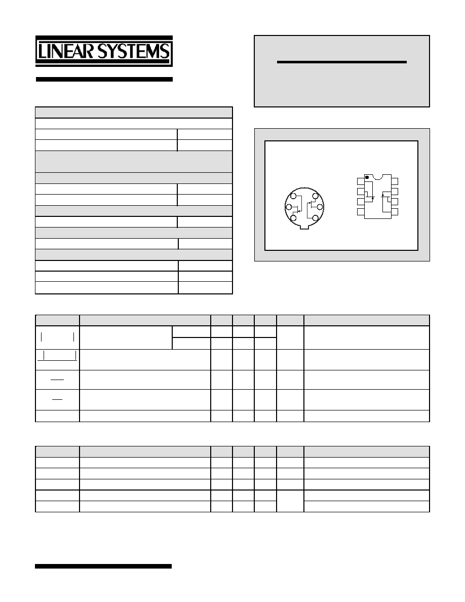
SST SERIES
1
2
3
4
8
7
6
5
SOIC
S1
D1
G1
NC
NC
G2
D2
S2
U SERIES
5
BOTTOM VIEW
TO-71
1
2
3
6
7
D1
G1
S1
S2
D2
G2
Linear Integrated Systems
U/SST440,441
MONOLITHIC DUAL
N-CHANNEL JFET
Linear Integrated Systems
∑ 4042 Clipper Court ∑ Fremont, CA 94538 ∑ Tel: 510 490-9160 ∑ Fax: 510 353-0261
Linear Integrated Systems
∑ 4042 Clipper Court ∑ Fremont, CA 94538 ∑ Tel: 510 490-9160 ∑ Fax: 510 353-0261
ELECTRICAL CHARACTERISTICS CONTINUED @ 25 įC (unless otherwise stated)
SYMBOL
CHARACTERISTIC
MIN TYP MAX UNITS
CONDITIONS
g
fs
Forward
Transconductance
4.5
6
9
mS
g
os
Output
Conductance
70
200
ĶS
V
DS
= 10V, I
D
= 5mA, f = 1kHz
C
iss
Input
Capacitance
3
C
rss
Reverse Transfer Capacitance
1
pF V
DS
= 10V, I
D
= 5mA, f = 1MHz
e
n
Equivalent Input Noise Voltage
4
nV/Hz
V
DS
= 10V, I
D
= 5mA, f = 10kHz
1.
Absolute maximum ratings are limiting values above which serviceability may be impaired.
2.
Pulse Test: PW 300Ķs Duty Cycle 3%
3.
Assumes smaller value in numerator.
Information furnished by Linear Integrated Systems is believed to be accurate and reliable. However, no responsibility is assumed for its
use; nor for any infringement of patents or other rights of third parties which may result from its use. No license is granted by implicatio
otherwise under any patent or patent rights of Linear Integrated Systems.
n or
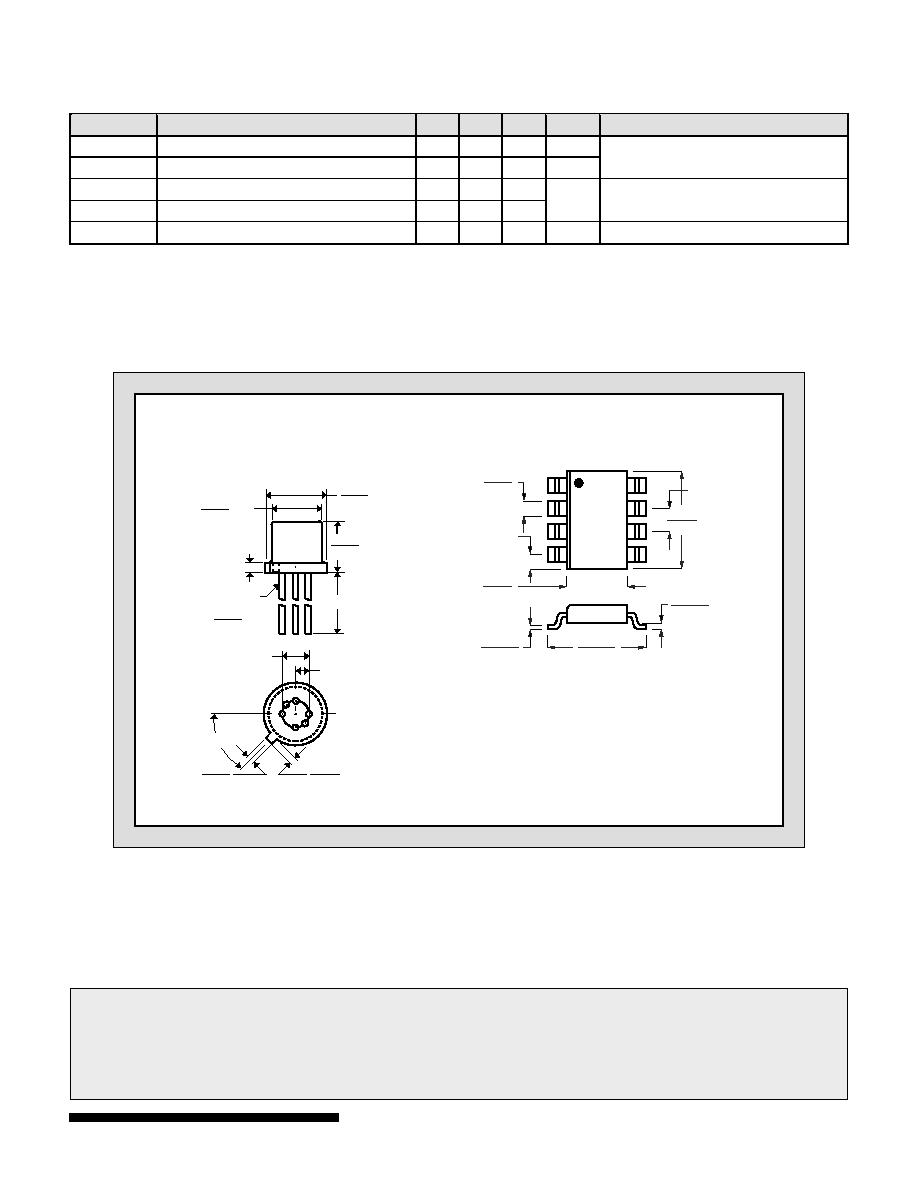
1
SOIC
2
3
4
5
6
7
8
DIMENSIONS IN
INCHES
0.2284
0.2440
0.189
0.196
0.0075
0.0098
0.021
0.014
0.018
0.050
0.0040
0.0098
0.150
0.157
TO-71
Six Lead
0.230
0.209
DIA.
DIA.
0.195
0.175
0.030
MAX.
0.500 MIN.
0.150
0.115
0.019
0.016
DIA.
6 LEADS
3
2
1
5
6
0.046
0.036
45į
0.048
0.028
0.100
0.050
7