
∑
LND1086/85
GENERAL DESCRIPTION
∑ Fixed Output Voltage 3.3, 2.9V, 2.5V
∑ Low Dropout Performance, 1V at Full
load
∑ Line Regulation Typically 0.015%
∑ Load Regulation Typically 0.1%
∑ Fast Transient Response
∑ TO-220
Packages
FEATURES
The LND1086/LND1085 Series 1.5/3.0A fixed
and adjustable voltage regulators are monolithic
integrated circuits designed to power the new
generation of microprocessors for use in
applications requiring a well regulated positive
output voltage with low input-output differential
voltage requirements and output voltage 3.3, 2.9V
or 2.5V. Outstanding features include full power
usage up to 1.5/3.0A of load current, internal
current limiting and thermal shutdown. Other
fixed versions are also available V
out
=2.0V to
4.0V. Please consult Linear Dimensions for more
information.
APPLICATIONS
∑ Microprocessor
Supplies
∑ Post Regulators for Switching
Supplies
∑ High Current Regulators
∑ 5V to 3.XXV for Pentium
Processors
∑ 3.3V to 2.5V for Portable Pentium
Processor
∑ Power PC Series Power Supplies
1.5 A / 3 A Low Dropout Voltage Regulators
DEVICE SELECTION GUIDE
Device
V
Out
(V)
I
Out
(A)
LND1086
3.3, 2.9, 2.5
1.5
LND1085
3.3, 2.9,2.5
3.0
FIXEDVOLTAGE REGULATOR
∑ Linear Dimensions, Inc. ∑ 445 East Ohio Street, Chicago IL 60611 USA ∑ tel 312.321.1810 ∑ fax 312.321.1830 ∑
www.lineardimensions.com
∑
DATA SHEET

SYMBOL
PARAMETER
MAXIMUM
UNITS
V
IN
Input Voltage
6
V
Po
Power Dissipation
Internally Limited
W
JC
Thermal resistance Junction to Case
3
JA
Thermal Resistance Junction to Ambient
50
∫C/W
T
J
Operating Junction Temperature Range
Control Section
Power Transistor
0 to 125
0 to 150
T
STG
Storage Temperature
-65 to 150
T
LEAD
Lead Temperature(soldering,10 sec)
260
∫C
ABSOLUTE MAXIMUM RATING
LND1085/86
PACKAGE INFORMATION
T Package TO≠220 Plastic
K PackageTO-3 Metal Can
P Package TO≠3P Plastic
Front View
Bottom View
Front View
BLOCK DIAGRAM
∑ Linear Dimensions, Inc. ∑ 445 East Ohio Street, Chicago IL 60611 USA ∑ tel 312.321.1810 ∑ fax 312.321.1830 ∑
www.lineardimensions.com
∑
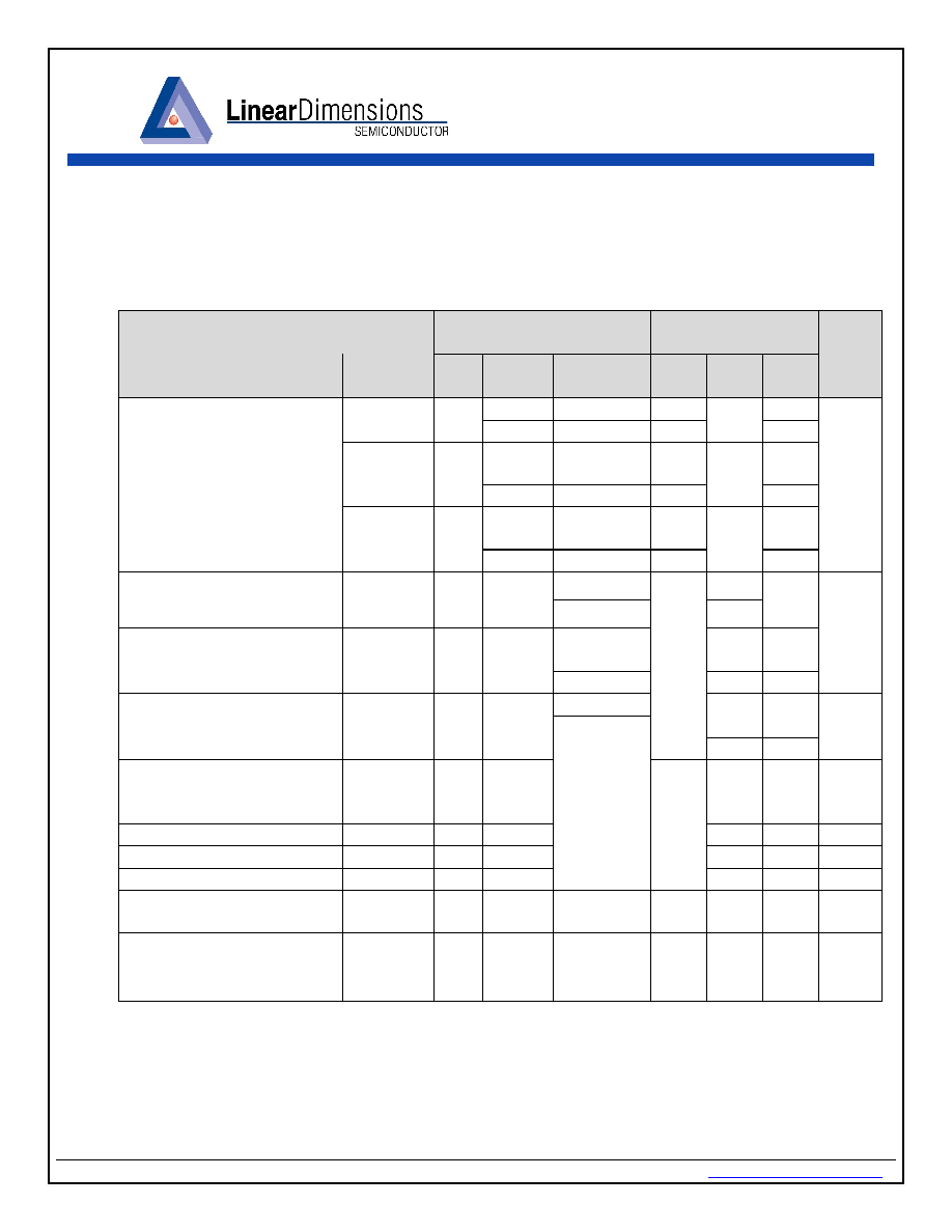
LND1085/86
(V
IN
=4.75 V to 5.25 V; I
o
=10mA to 3.0A(LND1085) ; I
o
= 10mA to 1.5 A(LND1086), Unless otherwise
specified)
Test Conditions
Test Limits
Parameter
Symbol
V
in
I
o
T
j
(3)
Min
Typ
Max
Units
10mA
25
∞C
3.267
3.333
V
o
5V
Over temp.
3.234
3.3
3.366
10mA
25
∞C
2.871
2.929
V
o
5V
Over temp.
2.842
2.9
2.958
10mA
25
∞C
2.475
2.525
Output Voltage
LND1086-3.3/LND1085-3.3
LND1086-2.9/LND1085-2.9
LND1086-2.5/LND1085-2.5
V
o
5V
Over temp.
2.450
2.5
2.550
V
25
∞C
0.015
Line Regulation(1)
REG
(Line)
10mA
Over temp.
0.035
0.2
25
∞C
0.1
0.3
Load regulation(1)
REG
(Load)
5V
Over temp
0.2
0.4
%
25
∞C
1.0
Dropout Voltage
Vout=2%
V
D
1.1
1.3
V
Current surge Limit
LND1085
LND1086
I
S
4.5
2.5
A
Quiescent current
I
Q
5V
10
16
mA
Temperature Coefficient
T
C
0.005
%/
∞C
Temperature Stability
T
S
5V
0.5A
Over temp.
0.5
%
RMS Output Noise(2)
V
N
25
∞C
0.003
%V
o
Ripple Rejection ratio
LND1085
LND1086
R
A
5V
3.0A
1.5A
Over temp.
60
72
dB
(1) Low duty cycle pulse testing
(2) Bandwidth of 10 Hz to 10kHz
(3) Over temp.= over specified operating junction temperature range.
ELECTRICAL
CHARACTERISTICS
∑ Linear Dimensions, Inc. ∑ 445 East Ohio Street, Chicago IL 60611 USA ∑ tel 312.321.1810 ∑ fax 312.321.1830 ∑
www.lineardimensions.com
∑
LND1085/86
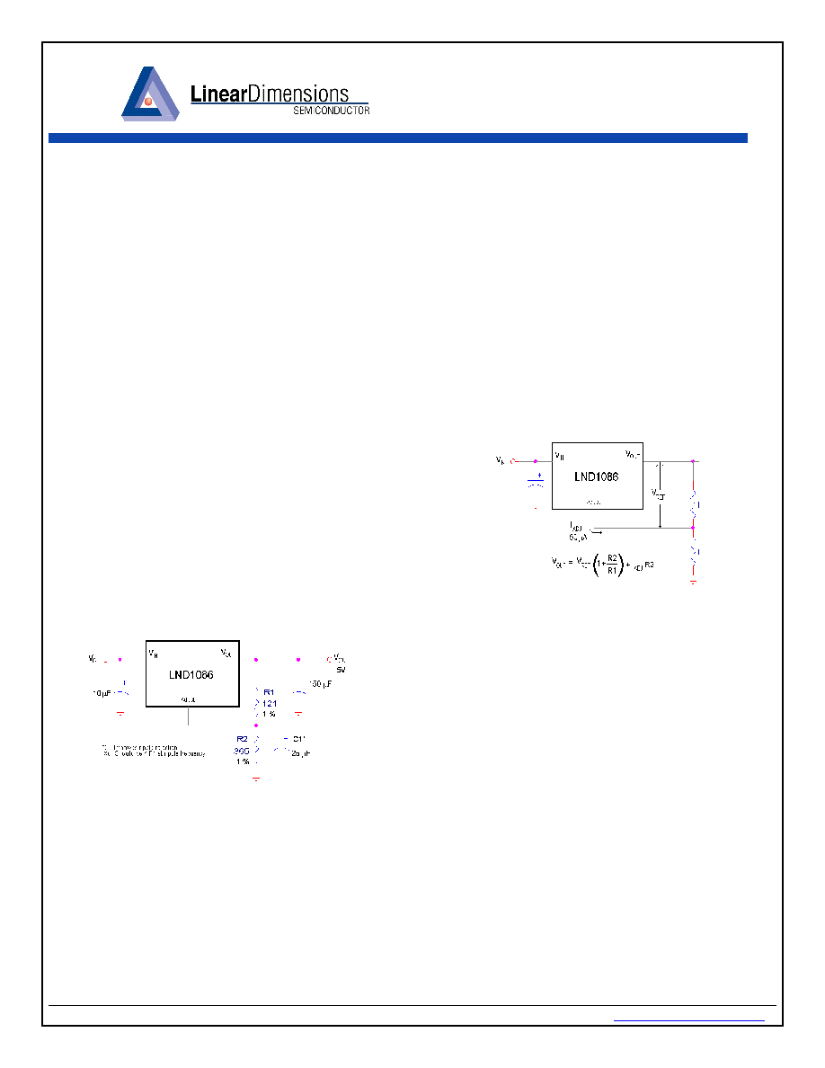
APPLICATIONS INFORMATION
The LND1086 family of three-terminal
adjustable regulators is easy to use and has all
the protection features that are expected in
high performance voltage regulators.
Stability
The circuit design used in the LND1086 series
requires the use of an output capacitor as part
of the device frequency compensation. The
addition of 150
µF aluminum electrolytic or a
22
µF solid tantalum on the output will ensure
stability for all operating conditions.
Output Voltage
The LND1086 develops a 1.25V reference
voltage between the Output pin and the Adjust
pin (Figure 1). Placing a resistor between
these two terminals causes a constant current
to flow through R1 and down though R2 to set
the output voltage. In general R1 is chosen so
that this current is the specified minimum load
current of 10mA. The current out of the Adjust
pin is small as compared to the current from
R1 and can be ignored. For fixed voltage
devices R1 and R2 are included in the device.
Microsecond surge currents of 10A to 20A
can be handled by the internal diode
between the Output pin and the Input pin of
the device. In normal operations it is difficult
to get those values of surge currents even
with the use of large output capacitance.
Only with high value output capacitors, such
as 1000 to 5000µF and with the Input pin
instantaneously shorted to ground, can
damage occur. A diode from output to input
is recommended (Figure 2).
Protection Diodes
In normal operation LND1086 family does not
need any protection diodes between the
adjustment pin and the output and from the
output to the input to prevent die
overstresses. Internal resistors are limiting
the internal current paths on the ADJ pin.
Therefore even with bypass capacitors on
the adjust pin no protection diode is needed
to ensure device safety under short-circuit
conditions
Thermal Considerations
The LND1086 series have internal power and
thermal-limiting circuitry designed to protect
the device under overload conditions.
However, maximum junction temperature
ratings should not be exceeded under
continuous normal load conditions. Careful
consideration must be given to all sources of
thermal resistance from junction to ambient,
including junction-to-case, case to-heat sink
interface and heat sink resistance itself.
∑ Linear Dimensions, Inc. ∑ 445 East Ohio Street, Chicago IL 60611 USA ∑ tel 312.321.1810 ∑ fax 312.321.1830 ∑
www.lineardimensions.com
∑
Figure 1. Output Voltage
Figure 2. Protection Diodes

Improving ripple rejection 1.2V to 15v adjustable regulator
5V regulator with shutdown Automatic light control
LND1085/86
TYPICAL APPLICATIONS
∑ Linear Dimensions, Inc. ∑ 445 East Ohio Street, Chicago IL 60611 USA ∑ tel 312.321.1810 ∑ fax 312.321.1830 ∑
www.lineardimensions.com
∑