∑
LND1117
DATA SHEET
GENERAL DESCRIPTION
∑ Adjustable or Fixed Output
∑ Output Current of 800mA
∑ Low Dropout 700mV at 800mA output
current
∑ 0.015% Line Regulation
∑ 0.01%
Load
Regulation
∑ 100% Thermal limit Burn-In
∑ Fast Transient Response
∑ Remote
Sense
FEATURES
The LND1117 series of positive adjustable and
fixed regulators are designed to provide
800mA with higher efficiency than currently
available devices. All internal circuitry is
designed to operate down to 700 mV input to
output differential and the dropout voltage is
fully specified as a function of load current.
Dropout voltage of the device is 100mV at light
loads and rising to 700mV at maximum output
current. A second low current input is required
to achieve this dropout. The LND1117 can
also be used as a single supply device( 3 pin
version). On-chip trimming adjusts the
reference voltage to 1%.
APPLICATIONS
∑ High Efficiency Linear Regulators
∑ Post Regulators for Switching
Supplies
∑ Adjustable
Power
Supply
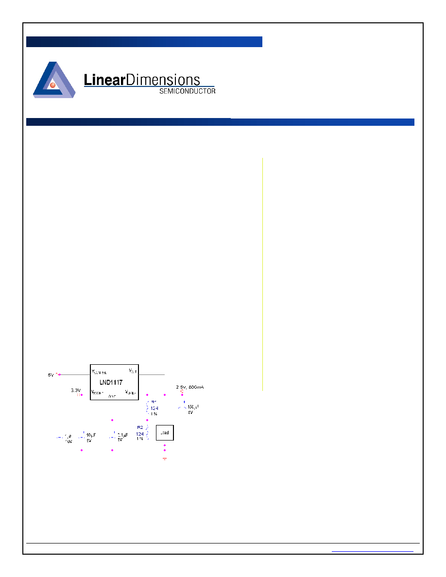
800mA Low Dropout Voltage Regulator
TYPICAL APPLICATION DATA
V
OUT
= V
REF
(1+R2/R1) +I
ADJ
R2
2.5 V, 800mA Regulator
∑ Linear Dimensions, Inc. ∑ 445 East Ohio Street, Chicago IL 60611 USA ∑ tel 312.321.1810 ∑ fax 312.321.1830 ∑
www.lineardimensions.com
∑

SYMBOL
PARAMETER
MAXIMUM
UNITS
P
D
Power Dissipation
Internally Limited
W
V
IN
Input Voltage
Vpower
Vcontrol
7
13
V
T
J
Operating Junction Temperature
Range
Control Section
Power Transistor
0 to 125
0 to 150
T
STG
Storage Temperature
-65 to 150
T
LEAD
Lead Temperature
(Soldering,10 sec)
300
∫C
DEVICE
OUTPUT VOLTAGE
LND1117
Adj.
LND1117-1.5
1.5V
LND1117-2.5
2.5V
LND1117-2.85
2.85V
LND1117-3.0
3.0V
LND1117-3.3
3.3V
LND1117-3.5
3.5V
LND1117-5.0
5.0V
Note 1: Other fixed versions are available Vout=1.5V to 5.0V
ABSOLUTE MAXIMUM RATING
LND1117
DEVICE SELECTION GUIDE (note 1)
PACKAGE INFORMATION
3 LEAD TO ≠220 (Front view)
5 LEAD TO ≠220 (Front View)
Vpower
Vcontrol
OUTPUT
ADJ/GND
SENSE
∑ Linear Dimensions, Inc. ∑ 445 East Ohio Street, Chicago IL 60611 USA ∑ tel 312.321.1810 ∑ fax 312.321.1830 ∑
www.lineardimensions.com
∑
V
IN
V
OUT
ADJ/GND

LND1117
Parameter
Device
Test Conditions
Min
Typ
Max
Units
Reference
Voltage
LND1117
Vcontrol=2.75V, Vpower=2V,I load=10mA
Vcontrol=2.7V to 12V
Vpower=3.3V to 5.5V, Iload=10mA to 800mA
*
1.238
1.230
1.250
1.250
1.262
1.270
V
Vcontrol=4V, Vpower=2V
Vcontrol=3V,Vpower2.3, Iload= 0mA to
800mA
*
1.485
1.475
1.500
1.500
1.515
1.525
V
Vcontrol=5V, Vpower=3.3V
Vcontrol=4V, Vpower 3.3, I load= 0mA to
800mA
*
2.475
2.460
2.500
2.500
2.525
2.540
V
Vcontrol=5.35V, Vpower=3.35V
Vcontrol=4.4V, Vpower3.7, I load= 0mA to
800mA
*
2.821
2.805
2.850
2.850
2.879
2.895
V
Vcontrol=5.5V, Vpower=3.5V
Vcontrol=4.5V, Vpower3.8 I load= 0mA to
800mA
*
2.970
2.950
3.000
3.000
3.030
3.050
V
Vcontrol=5.8V, Vpower=3.8V
Vcontrol=4.8V, Vpower4.1, I load= 0mA to
800mA
*
3.267
3.247
3.300
3.300
3.333
3.353
V
Vcontrol=6V, Vpower=4V
Vcontrol=6.5V, Vpower5.8, I load= 0mA to
800mA
*
3.465
3.445
3.500
3.500
3.535
3.555
V
Output Voltage
LND1117-1.5
LND1117-2.5
LND1117-
2.85
LND1117-3.0
LND1117-3.5
LND1117-5.0
Vcontrol=7.5V, Vpower=5.5V
Vcontrol=6.5V, Vpower5.8, I load= 0mA to
800mA
*
4.950
4.920
5.000
5.000
5.050
5.080
V
Line Regulation
All
Iload=10mA(1.5V+Vout)<=Vcontrol <= 12V,
0.8V<=(Vpower-Vout)<=5.5V
*
0.04
0.20
%
Load
Regulation
All
Vcontrol=Vout+2.5V, Vpower=Vout=0.8V I load
=10mA to 800mA
*
0.08
0.40
%
Minimum Load
Current(Note 2)
LND1117
Vcontrol=5V,Vpower=3.3V Vadj=0V
*
1.7
5
mA
Control Pin
Current (Note
3)
All
Vcontrol=Vout+2.5V,
Vpower=Vout+0.8V,Iload=10mA to 800mA
*
10
20
mA
Ground Pin
Current
LND1117-
1.5/
-2.5/2.85/-
3.0/-3.3/-3.5/-
5.0
Vcontrol=Vout+2.5V,Vpower=Vout +0.8V,
Iload=10mA to 800mA
*
6
10
mA
Adjust Pin
Current
LND1117
Vcontrol=2.75V, Vpower==2.05V Iload=10mA
*
50
120
µA
Current Limit
All
(Vin-Vout)=3V
*
800
1100
mA
Ripple
Rejection
All
Vcontrol= Vpower=Vout +2.5V,Vripple=1Vpp
Iload=400mA
*
60
75
dB
ELECTRICAL CHARACTERISTICS
∑ Linear Dimensions, Inc. ∑ 445 East Ohio Street, Chicago IL 60611 USA ∑ tel 312.321.1810 ∑ fax 312.321.1830 ∑
www.lineardimensions.com
∑

Parameter
Device
Test Conditions
Min
Typ
Max
Units
Thermal
Regulation
LND1117
T
A =
25∫C,30ms pulse
0.003
%/W
Dropout Voltage
Control Input
(Vcontrol-Vout)
All
Vpower=Vout+0.8V, Iload=10mA
Vpower=Vout+0.8V, Iload=800mA
*
1.00
1.15
1.15
1.30
V
Power Input
(Vpower-Vout)
All
Vcontrol= Vout+2.5V, Iload=800mA
*
0.55
0.70
V
The *denotes the specifications which apply over the full temperature range.
Note 1: Unless otherwise specified Vout=Vsense. For LND1117(adj) Vadj=OV
Note 2: For the adjustable device the minimum load current is the minimum current required to maintain regulation. Normally the
current in the resistor divider used to set the output voltage is selected to meet the minimum load current requirement.
Note3: The control pin current is the drive current required for the output transistor. The current will track output current with a ratio of
about 1:100.
Note4: The dropout voltage for the LND1117 is caused by either minimum control voltage or minimum power voltage. The
specifications represent the minimum input/output voltage required to maintain 1% regulation.
LND1117
PIN FUNCTIONS (5-LEAD)
Sense (Pin 1): This pin is the positive side of
the reference voltage. With this pin it is
possible to Kelvin sense the output voltage at
the load.
Adjust (Pin 2): This pin is the negative side of
the reference voltage. Adding a small bypass
capacitor from the Adjust pin to ground improves
the transient response. For fixed voltage
devices the Adjust pin is also brought out to
allow the user to add a bypass capacitor.
GND (Pin 2): For fixed voltage devices this is
the bottom of the resistor divider that sets the
output voltage.
Vpower (Pin 5): This pin is the collector of the
power transistor. The output load current is
supplied through this pin. The voltage at this pin
must be 0.7V greater than the output voltage for
the device to regulate.
Vcontrol (pin 4): This pin is the supply pin for the
control circuitry. The current flow into this pin will
be about 1% of the output current. The voltage at
this pin must be 1.3V greater than the output
voltage for the device to regulate.
Output (Pin 3): This is the power output of the
device.
BLOCK DIAGRAM
∑ Linear Dimensions, Inc. ∑ 445 East Ohio Street, Chicago IL 60611 USA ∑ tel 312.321.1810 ∑ fax 312.321.1830 ∑
www.lineardimensions.com
∑

LND1117
Linear Dimensions, Inc. 445
APPLICATION INFORMATION
The LND1117 is designed to make use of
multiple power supplies, to reduce the
dropout voltage. One of the advantages of
the two supply approach is maximizing the
efficiency.
The second supply is at least 1V greater than
output voltage and is providing the power for
the NPN output transistor. This allows the
NPN output transistor to be driven into
saturation. For the control voltage the
current requirement is small and equal to
about 1% of the output current. This drive
current becomes part of the output current.
The maximum voltage on the control pin is
12V. The maximum voltage at the Power Pin
is 7V. By trying the control and power inputs
together the LND1117 can also be operated
as a single supply device. In single supply
operation the dropout will be determined by
the minimum control voltage.
Both the fixed and adjustable versions have
remote sense pins, permitting very accurate
regulation of output voltage. As a result, over
an output current range of 100mA to 800mA,
the typical load regulation is less than1mV.
For the fixed voltages the adjust pin is
brought out allowing the user to improve
transient response by bypassing the internal
resistor divider. Optimum transient response
is provided using a capacitor in the range of
0.1µF to 1µF for bypassing the Adjust pin. In
addition to the enhancements mentioned, the
reference accuracy has been improved a
factor or two with a guaranteed initial
tolerance of ±1% at 25∫C and 1.6% accuracy
over the full temperature and load current
range.
Typical applications for the LND1117 include
3.3V to 2.5V conversion with a 5V control
supply, 5V to 4.2V conversion with a 12V
control supply. The device is fully protected
against overcurrent and overtemperature
conditions.
Grounding and Output Sensing
The LND1117 allows true Kelvin sensing for
both the high and low side of the load. As a
result the voltage regulation at the load can be
easily optimized. Voltage drops due to
parasitic resistance between the regulator and
the load can be placed inside the regulation
loop. The advantages of remote sensing are
illustrated in figures 1 through 3. Figure 1
shows the device connected as a conventional
3 terminal regulator with the sense lead
connected directly to the output of the device.
R
P
is the parasitic resistanceof the connections
between the device and the load.Trace A of
figure 3, illiustrates the effect of R
P
. Figure 2,
shows the device connected to take advantage
of the remote sense feature. The sense pin
and the top of the resistor divider are
connected to the top of the load: the bottom of
the load. The effect on output regulation can
be seen in trace B of figure 3.
It is important to note that the voltage drops
due to Rp are not eliminated, they will add to
the dropout voltage of the regulator regardless.
The LND1117 can control the voltage at the
load as long as the input-output voltage is
greater than the total of the dropout voltage of
the device plus the voltage drop across R
P.
Stability
The circuit design used in the LND1117 series
requires the use of an output capacitor as part
of the device frequency compensation. The
addition of 150µF aluminum electrolytic or a
22µF solid tantalum on the output will ensure
stability for all operating conditions.
∑ Linear Dimensions, Inc. ∑ 445 East Ohio Street, Chicago IL 60611 USA ∑ tel 312.321.1810 ∑ fax 312.321.1830 ∑
www.lineardimensions.com
∑