 | –≠–ª–µ–∫—Ç—Ä–æ–Ω–Ω—ã–π –∫–æ–º–ø–æ–Ω–µ–Ω—Ç: 1698 | –°–∫–∞—á–∞—Ç—å:  PDF PDF  ZIP ZIP |
1
LTC1698
1698f
APPLICATIO S
U
DESCRIPTIO
U
FEATURES
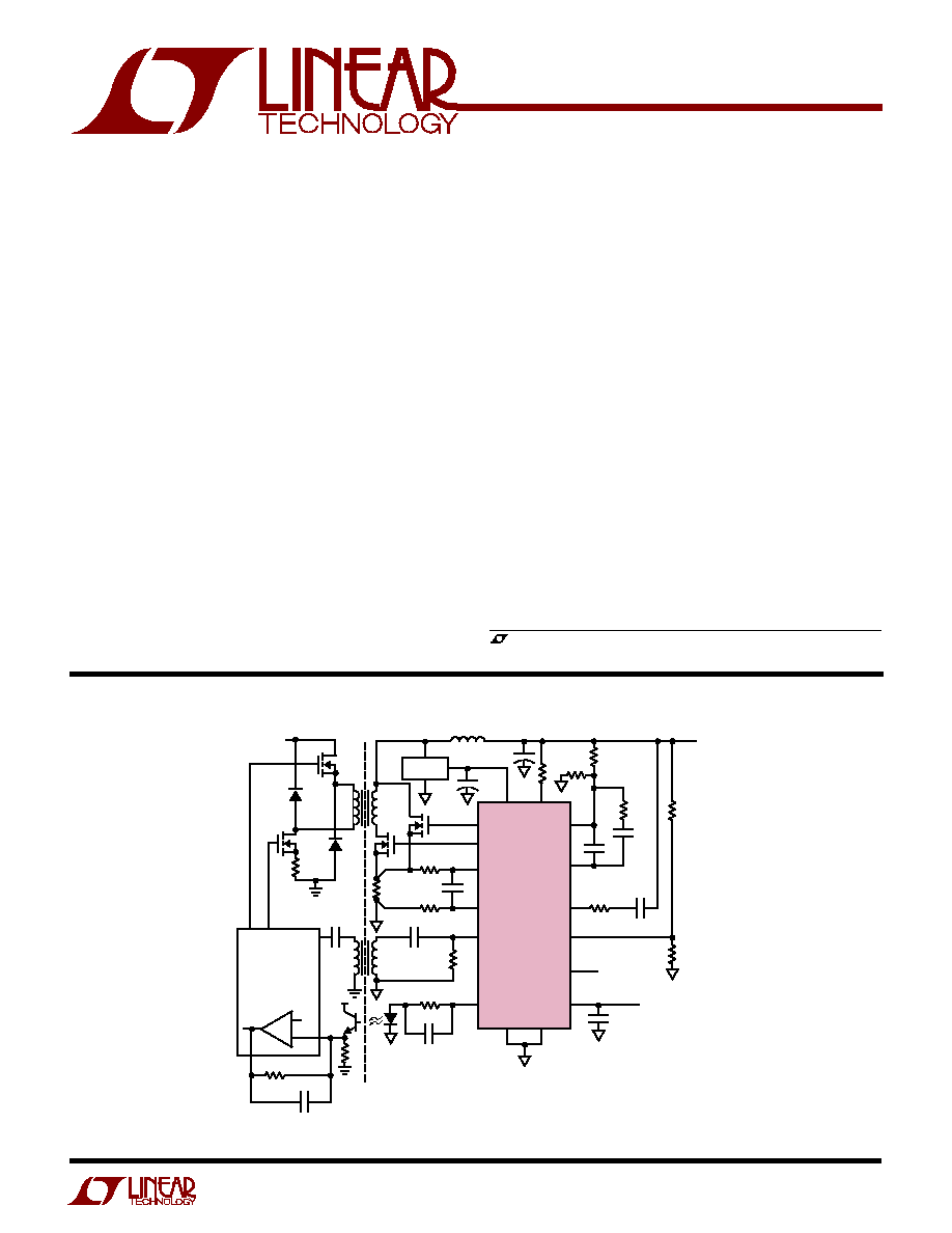
TYPICAL APPLICATIO
U
The LTC
Æ
1698 is a precision secondary-side forward
converter controller that synchronously drives external
N-channel MOSFETs. It is designed for use with the
LT
Æ
3781 primary-side synchronous forward converter
controller to create a completely isolated power supply.
The LT3781 synchronizes the LTC1698 through a small
pulse transformer and the LTC1698 drives a feedback
optocoupler to close the feedback loop. Output accuracy
of
±
0.8% and high efficiency over a wide range of load
currents are obtained.
The LTC1698 provides accurate secondary-side current
limit using an external current sense resistor. The input
voltage at the MARGIN pin provides
±
5% output voltage
adjustment. A power good flag and overvoltage input are
provided to ensure proper power supply conditions. An
auxiliary 3.3V logic supply is included that supplies up to
10mA of output current.
Isolated Secondary
Synchronous Rectifier Controller
s
High Efficiency Over Wide Load Current Range
s
±
0.8% Output Voltage Accuracy
s
Dual N-Channel MOSFET Synchronous Drivers
s
Pulse Transformer Synchronization
s
Optocoupler Feedback Driver
s
Programmable Current Limit Protection
s
±
5% Margin Output Voltage Adjustment
s
Adjustable Overvoltage Fault Protection
s
Power Good Flag
s
Auxiliary 3.3V Logic Supply
s
Available in 16-Lead SSOP and SO Packages
s
48V Input Isolated DC/DC Converters
s
Isolated Telecommunication Power Systems
s
Distributed Power Step-Down Converters
s
Industrial Control Systems
s
Automotive and Heavy Equipment
Figure 1. Simplified 2-Transistor Isolated Forward Converter
, LTC and LT are registered trademarks of Linear Technology Corporation.
+
+
CG
V
DD
PWRGD
LTC1698
PGND
GND
2
8
C
FB
C
C
C
CILM
R
C
V
OUT
R
CILM
R2
R5
R4
R1
L1
6
13
9
7
14
C
OUT
1
10
Q4
V
IN
36V to 72V
Q3
T1
∑
∑
Q1
D1
Q2
R
PRISEN
T2
FG
16
I
SNS
R
SECSEN
12
I
SNSGND
11
SYNC
V
FB
V
COMP
V
AUX
I
COMP
OVPIN
MARGIN
V
MARGIN
O.1
µ
F
1681 F01
V
AUX
3.3V
10mA
15
OPTODRV
PLEASE REFER TO FIGURE 12 IN THE TYPICAL APPLICATIONS
SECTION FOR THE COMPLETE 3.3V/15A APPLICATION SCHEMATIC
5
3
4
R
SYNC
R
K
R
E
ISOLATION
BOUNDARY
R
F
REF
V
FB
SG
TG
BG
LT3781
V
C
C
SYNC
C
K
C
F
V
DD
BIAS
C
SG
+
≠
D2
∑
∑

2
LTC1698
1698f
(Note 1)
V
DD
, PWRGD ....................................................... 13.2V
Input Voltage
MARGIN, V
FB
, OVPIN, I
SNSGND
, I
SNS
... ≠ 0.3V to 5.3V
SYNC ..................................................... ≠ 14V to 14V
Output Voltage
V
COMP
, I
COMP
(Note 2) ......................... ≠ 0.3V to 5.3V
Power Dissipation .............................................. 500mW
Operating Temperature Range
LTC1698E (Note 3) ............................ ≠ 40
∞
C to 85
∞
C
LTC1698I ........................................... ≠ 40
∞
C to 85
∞
C
Storage Temperature Range ................. ≠ 65
∞
C to 150
∞
C
Lead Temperature (Soldering, 10 sec).................. 300
∞
C
ABSOLUTE
M
AXI
M
U
M
RATINGS
W
W
W
U
PACKAGE/ORDER I
N
FOR
M
ATIO
N
W
U
U
ORDER PART
NUMBER
LTC1698EGN
LTC1698ES
LTC1698IGN
LTC1698IS
T
JMAX
= 125
∞
C,
JA
= 130
∞
C/W (GN)
T
JMAX
= 125
∞
C,
JA
= 110
∞
C/W (SO)
GN PACKAGE
16-LEAD PLASTIC SSOP
S PACKAGE
16-LEAD PLASTIC SO
1
2
3
4
5
6
7
8
TOP VIEW
16
15
14
13
12
11
10
9
V
DD
CG
PGND
GND
OPTODRV
V
COMP
MARGIN
V
FB
FG
SYNC
V
AUX
I
COMP
I
SNS
I
SNSGND
PWRGD
OVPIN
The
q
indicates specifications which apply over the full operating
temperature range, otherwise specifications are at T
A
= 25
∞
C. V
DD
= 8V, unless otherwise noted. (Note 4)
ELECTRICAL CHARACTERISTICS
Consult LTC Marketing for parts specified with wider operating temperature ranges.
SYMBOL
PARAMETER
CONDITIONS
MIN
TYP
MAX
UNITS
V
DD
Supply Voltage
q
6
8
12.6
V
V
UVLO
Undervoltage Lockout
4
V
I
VDD
V
DD
Supply Current
V
FB
, OVPIN, V
ISNS
, V
ISNSGND
= 0V,
C
FG
= C
CG
= 1000pF, C
VAUX
= 0.1
µ
F,
V
SYNC
= 0V
q
1.8
4
mA
f
SYNC
= 100kHz (Note 5)
5.0
mA
MARGIN and Error Amplifier
V
FB
Feedback Voltage
MARGIN = Open, V
COMP
= 1V (Note 7)
1.223
1.233
1.243
V
q
1.215
1.233
1.251
V
I
VFB
Feedback Input Current
V
FB
= 1.233V
q
0.05
1
µ
A
V
MARGIN
MARGIN Voltage
MARGIN = Open
1.65
V
R
MARGIN
MARGIN Input Resistance
16.5
k
V
FB
Feedback Voltage Adjustment
V
MARGIN
= 3.3V
q
4
5
6
%
V
MARGIN
= 0V
q
≠ 6
≠ 5
≠ 4
%
G
ERR
Error Amplifier Open-Loop DC Gain
V
COMP
= 0.8V to 1.2V, Load = 2k
, 100pF
q
65
90
dB
BW
ERR
Error Amplifier Unity-Gain Bandwidth
No Load (Note 6)
2
MHz
V
CLAMP
Error Amplifier Output Clamp Voltage
V
FB
= 0V
2
V
I
VCOMP
Error Amplifier Source Current
V
FB
= 0V
q
≠ 25
≠ 10
mA
Error Amplifier Sink Current
V
FB
= 5V, V
COMP
= 1.233V
q
3
7
mA
OPTODRV
G
OPTO
Opto Driver DC Gain
OVPIN, V
ISNS
, V
ISNSGND
= 0V
q
4.75
5
5.25
V/V
BW
OPTO
Opto Driver Unity-Gain Bandwidth
No Load (Note 6)
1
MHz
V
OPTOHIGH
Opto Driver Output High Voltage
V
FB
, OVPIN, V
ISNSGND
= 0V, V
ISNS
= ≠ 50mV,
I
OPTODRV
= ≠10mA
q
4
5
V
I
OPTOSC
Opto Driver Output Short-Circuit Current
OVPIN, V
ISNSGND
, V
ISNS
= 0V, V
FB
= 1.233V
q
≠ 50
≠ 25
≠ 10
mA
GN PART MARKING
1698
1698I

3
LTC1698
1698f
The
q
indicates specifications which apply over the full operating
temperature range, otherwise specifications are at T
A
= 25
∞
C. V
DD
= 8V, unless otherwise noted. (Note 4)
ELECTRICAL CHARACTERISTICS
Note 1: Absolute Maximum Ratings are those values beyond which the life
of a device may be impaired. All voltages refer to GND.
Note 2: The LTC1698 incorporates a 5V linear regulator to power internal
circuitry. Driving these pins above 5.3V may cause excessive current flow.
Guaranteed by design and not subject to test.
Note 3: The LTC1698E is guaranteed to meet performance specifications
from 0
∞
C to 70
∞
C. Specifications over the ≠ 40
∞
C to 85
∞
C operating
temperature range are assured by design, characterization and correlation
with statistical process controls. For guaranteed performance to
specifications over the ≠40
∞
C to 85
∞
C range, the LTC1698I is available.
Note 4: All currents into device pins are positive; all currents out of the
device pins are negative. All voltages are referenced to ground unless
otherwise specified. For applications with V
DD
< 7V, refer to the Typical
Performance Characteristics.
Note 5: Supply current in active operation is dominated by the current
needed to charge and discharge the external FET gates. This will vary with
the LTC1698 operating frequency, supply voltage and the external FETs
used.
Note 6: This parameter is guaranteed by correlation and is not tested.
Note 7: V
FB
is tested in an op amp feedback loop which servos V
FB
to the
internal bandgap voltage.
Note 8: The current comparator output current varies linearly with
temperature.
Note 9: The PWRGD and OVP comparators incorporate 10mV of
hysteresis.
Note 10: The driver disable time-out is proportional to the SYNC period
within the frequency synchronization range.
SYMBOL PARAMETER
CONDITIONS
MIN
TYP
MAX
UNITS
V
AUX
V
AUX
Auxiliary Supply Voltage
C
VAUX
= 0.1
µ
F, I
LOAD
= 0mA to 10mA, V
DD
= 7V to 12.6V
q
3.135
3.320
3.465
V
Current Limit Amplifier
I
ISNSGND
I
SNSGND
Input Current
V
ISNSGND
= 0V
q
0.05
1
µ
A
I
ISNS
I
SNS
Input Current
V
ISNS
= 0V
q
0.05
1
µ
A
V
ILIMTH
Current Limit Threshold
V
ICOMP
= 2.5V, V
ISNSGND
= 0V
≠ 27.0
≠ 25
≠ 23.0
mV
(V
ISNS
≠ V
ISNSGND
)
q
≠ 27.5
≠ 25
≠ 22.5
mV
I
ICOMP
I
COMP
Source Current
V
ISNSGND
= 0V, V
ISNS
= ≠ 0.3V, V
ICOMP
= 2.5V (Note 8)
≠ 280
≠ 200
≠ 120
µ
A
q
≠ 370
≠ 200
≠ 80
µ
A
I
COMP
Sink Current
V
ISNSGND
= 0V, V
ISNS
= 0.3V, V
ICOMP
= 2.5V (Note 8)
120
200
280
µ
A
q
80
200
370
µ
A
g
mILIM
Current Limit Amplifier
V
ISNSGND
= 0V, V
ICOMP
= 2.5V, I
ICOMP
=
±
10
µ
A
q
2.2
3.5
5
millimho
Transconductance
G
ICOMP
Current Limit Amplifier
V
ICOMP
= 2.5V, No Load
q
48
60
dB
Open-Loop DC Gain
PWRGD and OVP Comparators
V
PWRGD
Percent Below V
FB
V
FB
, MARGIN = Open (Note 9)
q
≠ 9
≠ 6
≠ 3
%
I
PWRGD
Power Good Sink Current
V
FB
= 2V
q
10
µ
A
V
FB
= 0V
q
10
mA
V
OL
Power Good Output Low Voltage
I
PWRGD
= 3mA, V
FB
= 0V
q
0.4
V
V
OVPREF
OVPIN Threshold
V
FB
= V
ISNS
= V
ISNSGND
= 0V, OVPIN
(Note 9)
q
1.18
1.233
1.28
V
I
OVPIN
OVPIN Input Bias Current
V
OVPIN
= 1.233V
q
0.1
1
µ
A
t
PWRGD
Power Good Response Time
V
FB
q
1
2
5
ms
Power Bad Response Time
V
FB
q
0.5
1
2.5
ms
t
OVP
Overvoltage Response Time
V
OVPIN
, C
OPTODRV
= 0.1
µ
F
q
5
20
µ
s
SYNC and Drivers
V
PT
SYNC Input Positive Threshold
q
1
1.6
2.2
V
V
NT
SYNC Input Negative Threshold
q
≠ 2.2
≠1.6
≠1
V
I
SYNC
SYNC Input Current
V
SYNC
=
±
10V
q
1
50
µ
A
f
SYNC
SYNC Frequency Range
C
FG
= C
CG
= 1000pF, V
SYNC
=
±
5V
q
50
400
kHz
t
d
SYNC Input to Driver Output Delay
C
FG
= C
CG
= 1000pF, f
SYNC
= 100kHz, V
SYNC
=
±
5V
q
40
90
ns
t
SYNC
Minimum SYNC Pulse Width
f
SYNC
= 100kHz, V
SYNC
=
±
10V (Note 6)
q
75
ns
t
r
, t
f
Driver Rise and Fall Time
C
FG
= C
CG
= 1000pF, f
SYNC
= 100kHz, V
SYNC
=
±
5V,
q
10
40
ns
10% to 90%
t
DDIS
Driver Disable Time-Out
C
FG
= C
CG
= 1000pF, f
SYNC
= 100kHz, V
SYNC
=
±
5V
Measured from CG
(Note 10)
q
10
15
20
µ
s
4
LTC1698
1698f
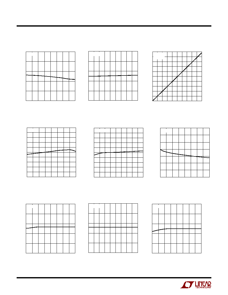
TYPICAL PERFOR A CE CHARACTERISTICS
U
W
V
FB
vs Temperature
TEMPERATURE (
∞
C)
≠50
V
FB
(V)
1.236
1.242
1.248
25
75
150
1698 G01
1.230
1.224
1.218
≠25
0
50
100 125
V
DD
= 8V
V
DD
(V)
5
1.218
V
FB
(V)
1.224
1.236
1.242
1.248
7
9
10
14
1698 G02
1.230
6
8
11
12
13
T
A
= 25
∞
C
V
MARGIN
(V)
0
V
FB
(V)
V
FB
(%)
1.245
1.270
1.295
2.64
1698 G03
1.221
1.196
1.233
1.258
1.282
1.208
1.184
1.171
1
3
5
≠1
≠3
0
2
4
≠2
≠4
≠5
0.66
0.33
1.32
0.99
1.98 2.31
2.97
1.65
3.3
V
DD
= 8V
T
A
= 25
∞
C
V
FB
vs V
DD
V
FB
vs V
MARGIN
I
SNS
Threshold vs Temperature
I
SNS
Threshold vs V
DD
Current Limit Amplifier g
m
vs Temperature
TEMPERATURE (
∞
C)
≠50
≠27.5
I
SNS
THRESHOLD (mV)
≠27.0
≠26.0
≠25.5
≠25.0
≠22.5
≠24.0
0
50
75
1698 G04
≠26.5
≠23.5
≠23.0
≠24.5
≠25
25
100 125
150
V
DD
= 8V
V
DD
(V)
5
≠27.5
I
SNS
THRESHOLD (mV)
≠27.0
≠26.0
≠25.5
≠25.0
≠22.5
≠24.0
8
7
10
11
1698 G05
≠26.5
≠23.5
≠23.0
≠24.5
6
9
12
13
14
T
A
= 25
∞
C
TEMPERATURE (
∞
C)
≠50
g
mILIM
(millimho)
3.8
4.2
4.6
100 125
1698 G06
3.4
3.0
≠25
25
0
50
75
150
2.6
2.2
5.0
V
DD
= 8V
OVPIN Threshold vs Temperature
OVPIN Threshold vs V
DD
Power Good Threshold
vs Temperature
TEMPERATURE (
∞
C)
≠50
OVPIN THRESHOLD (V)
1.24
1.26
1.28
25
75
150
1698 G07
1.22
1.20
1.18
≠25
0
50
100 125
V
DD
= 8V
V
DD
(V)
5
1.18
OVPIN THRESHOLD (V)
1.20
1.24
1.26
1.28
7
9
10
14
1698 G08
1.22
6
8
11
12
13
T
A
= 25
∞
C
TEMPERATURE (
∞
C)
≠50
POWER GOOD THRESHOLD (V)
V
FB
(%)
1.166
1.181
1.196
25
75
150
1698 G09
1.152
1.137
1.122
≠5.4
≠4.2
≠3.0
≠6.6
≠7.8
≠9.0
≠25
0
50
100 125
V
DD
= 8V

5
LTC1698
1698f
TYPICAL PERFOR A CE CHARACTERISTICS
U
W
V
AUX
vs Temperature
V
AUX
vs Line Voltage
V
AUX
vs Load Current
V
AUX
Short-Circuit Current
vs Temperature
V
AUX
Short-Circuit Current
vs V
DD
Opto Driver Load Regulation
Opto Driver Short-Circuit Current
vs Temperature
TEMPERATURE (
∞
C)
≠50
V
AUX
(V)
3.300
3.383
150
1698 G10
3.218
3.135
0
50
100
≠25
25
75
125
3.465
3.259
3.341
3.176
3.424
V
DD
= 8V
I
LOAD
= 0mA
V
DD
(V)
5
V
AUX
(V)
3.300
3.383
14
1698 G11
3.218
3.135
7
8
10
12
6
9
11
13
3.465
3.259
3.341
3.176
3.424
V
DD
= 8V
I
LOAD
= 0mA
LOAD CURRENT (mA)
0
V
AUX
(V)
3.300
3.383
10
9
1698 G12
3.218
3.135
2
3
5
7
1
4
6
8
3.465
3.259
3.341
3.176
3.424
V
DD
= 8V
T
A
= 25
∞
C
TEMPERATURE (
∞
C)
≠50
V
AUX
SHORT-CIRCUIT CURRENT (mA)
≠20
≠10
0
25
75
150
1698 G13
≠30
≠40
≠50
≠25
0
50
100 125
V
DD
= 8V
V
DD
(V)
5
V
AUX
SHORT-CIRCUIT CURRENT (mA)
≠20
≠10
0
8
10
14
1698 G14
≠30
≠40
≠50
6
7
9
11
12
13
T
A
= 25
∞
C
LOAD CURRENT (mA)
0
OPTO DRIVER OUTPUT VOLTAGE (V)
PERCENT (%)
3.006
3.018
3.030
8
1698 G15
2.994
2.982
3.000
3.012
3.024
2.988
2.976
2.970
0.2
0.6
1.0
≠0.2
≠0.6
0
0.4
0.8
≠0.4
≠0.8
≠1.0
2
1
4
3
6
7
9
5
10
V
DD
= 8V
T
A
= 25
∞
C
TEMPERATURE (
∞
C)
≠50
OPTO DRIVER SHORT-CIRCUIT CURRENT (mA)
≠30
≠20
150
1698 G16
≠40
≠50
0
50
100
≠25
25
75
125
≠10
≠35
≠25
≠45
≠15
V
DD
= 8V
V
OPTODRV
= 1.233V
Maximum OPTO Driver Output
Voltage vs Load Current
Maximum OPTO Driver Output
Voltage vs Temperature
LOAD CURRENT (mA)
0
MAXIMUM OPTO DRIVER OUTPUT VOLTAGE (V)
4
6
8
1698 G22
2
0
2
4
5
10
8
6
1
3
9
7
V
DD
= 10V
V
DD
= 8V
V
DD
= 7V
V
DD
= 6V
V
DD
= 5V
T
A
= 25
∞
C
V
COMP
= 0V
TEMPERATURE (
∞
C)
≠50
0
MAXIMUM OPTO DRIVER OUTPUT VOLTAGE (V)
2
4
6
8
≠25
0
25
50
1698 G23
75
100 125 150
V
DD
= 10V
V
DD
= 8V
V
DD
= 6V
V
DD
= 5V
V
COMP
= 0V
I
OPTODRV
= ≠10mA
V
DD
= 7V