 | –≠–ª–µ–∫—Ç—Ä–æ–Ω–Ω—ã–π –∫–æ–º–ø–æ–Ω–µ–Ω—Ç: 6300 | –°–∫–∞—á–∞—Ç—å:  PDF PDF  ZIP ZIP |
1
LT6300
500mA, 200MHz xDSL
Line Driver in 16-Lead SSOP Package
s
Exceeds All Requirements For Full Rate,
Downstream ADSL Line Drivers
s
Power Enhanced 16-Lead SSOP Package
s
Power Saving Adjustable Supply Current
s
±
500mA Minimum I
OUT
s
±
10.9V Output Swing, V
S
=
±
12V, R
L
= 100
s
±
10.7V Output Swing, V
S
=
±
12V, I
L
= 250mA
s
Low Distortion: ≠ 82dBc at 1MHz, 2V
P-P
Into 50
s
200MHz Gain Bandwidth
s
600V/
µ
s Slew Rate
s
Specified at
±
12V and
±
5V
s
High Efficiency ADSL, HDSL2, SHDSL Line Drivers
s
Buffers
s
Test Equipment Amplifiers
s
Cable Drivers
The LT
Æ
6300 is a 500mA minimum output current, dual op
amp with outstanding distortion performance. The ampli-
fiers are gain-of-ten stable, but can be easily compensated
for lower gains. The extended output swing allows for
lower supply rails to reduce system power. Supply current
is set with an external resistor to optimize power dissipa-
tion. The LT6300 features balanced, high impedance in-
puts with low input bias current and input offset voltage.
Active termination is easily implemented for further sys-
tem power reduction. Short-circuit protection and thermal
shutdown insure the device's ruggedness.
The outputs drive a 100
load to
±
10.9V with
±
12V
supplies, and
±
10.7V with a 250mA load. The LT6300 is a
functional replacement for the LT1739 and LT1794 in
xDSL line driver applications and requires no circuit
changes.
The LT6300 is available in the very small, thermally
enhanced, 16-lead SSOP package (same PCB area as the
SO-8 package) for maximum port density in line driver
applications.
, LTC and LT are registered trademarks of Linear Technology Corporation.
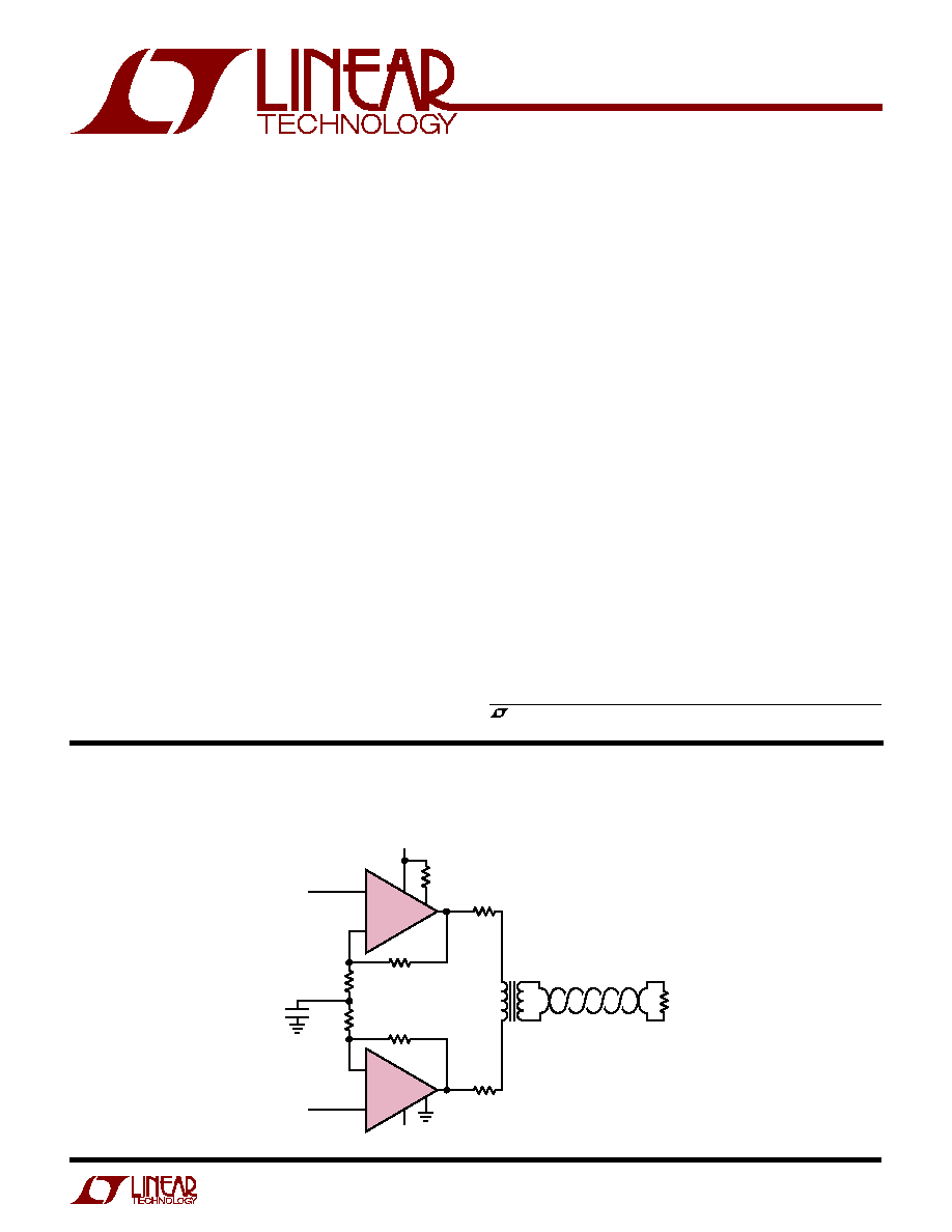
High Efficiency
±
12V Supply ADSL Line Driver
6300 TA01
+
≠
1/2
LT6300
≠IN
≠
+
1/2
LT6300
+IN
12V
SHDN
≠12V
12.7
24.9k
1:2*
110
1000pF
110
1k
1k
12.7
SHDNREF
100
*COILCRAFT X8390-A OR EQUIVALENT
I
SUPPLY
= 10mA PER AMPLIFIER
WITH R
SHDN
= 24.9k
∑
∑
FEATURES
DESCRIPTIO
U
APPLICATIO S
U
TYPICAL APPLICATIO
U

2
LT6300
ORDER PART
NUMBER
Supply Voltage (V
+
to V
≠
) .................................
±
13.5V
Input Current .....................................................
±
10mA
Output Short-Circuit Duration (Note 2) ........... Indefinite
Operating Temperature Range ............... ≠ 40
∞
C to 85
∞
C
Specified Temperature Range (Note 3) .. ≠ 40
∞
C to 85
∞
C
Junction Temperature .......................................... 150
∞
C
Storage Temperature Range ................. ≠ 65
∞
C to 150
∞
C
Lead Temperature (Soldering, 10 sec).................. 300
∞
C
LT6300CGN
LT6300IGN
Consult LTC Marketing for parts specified with wider operating temperature
ranges.
ABSOLUTE
M
AXI
M
U
M
RATINGS
W
W
W
U
PACKAGE/ORDER I
N
FOR
M
ATIO
N
W
U
U
(Note 1)
T
JMAX
= 150
∞
C,
JA
= 70
∞
C/W to 95
∞
C/W (Note 4)
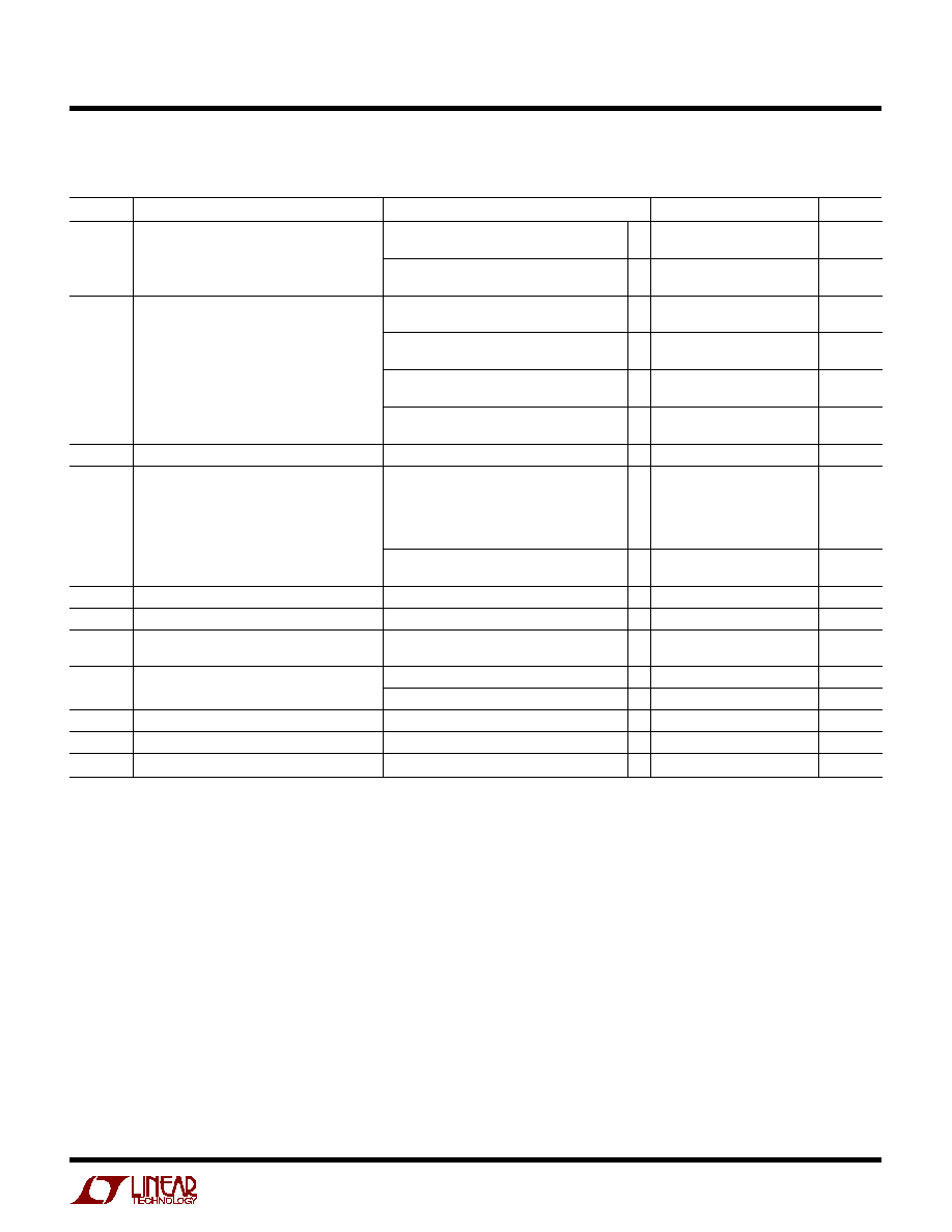
ELECTRICAL CHARACTERISTICS
The
q
denotes the specifications which apply over the full specified temperature range, otherwise specifications are at T
A
= 25
∞
C.
V
CM
= 0V, pulse tested,
±
5V
V
S
±
12V, V
SHDNREF
= 0V, R
BIAS
= 24.9k between V
+
and SHDN unless otherwise noted. (Note 3)
SYMBOL
PARAMETER
CONDITIONS
MIN
TYP
MAX
UNITS
V
OS
Input Offset Voltage
1
5.0
mV
q
7.5
mV
Input Offset Voltage Matching
0.3
5.0
mV
q
7.5
mV
Input Offset Voltage Drift
q
10
µ
V/
∞
C
I
OS
Input Offset Current
100
500
nA
q
800
nA
I
B
Input Bias Current
±
0.1
±
4
µ
A
q
±
6
µ
A
Input Bias Current Matching
100
500
nA
q
800
nA
e
n
Input Noise Voltage Density
f = 10kHz
8
nV/
Hz
i
n
Input Noise Current Density
f = 10kHz
0.8
pA/
Hz
R
IN
Input Resistance
V
CM
= (V
+
≠ 2V) to (V
≠
+ 2V)
q
5
50
M
Differential
6.5
M
C
IN
Input Capacitance
3
pF
Input Voltage Range (Positive)
(Note 5)
q
V
+
≠ 2
V
+
≠ 1
V
Input Voltage Range (Negative)
(Note 5)
q
V
≠
+ 1
V
≠
+ 2
V
CMRR
Common Mode Rejection Ratio
V
CM
= (V
+
≠ 2V) to (V
≠
+ 2V)
74
83
dB
q
66
dB
PSRR
Power Supply Rejection Ratio
V
S
=
±
4V to
±
12V
74
88
dB
q
66
dB
GN PART
MARKING
6300
6300I
1
2
3
4
5
6
7
8
TOP VIEW
16
15
14
13
12
11
10
9
V
≠
≠IN
+IN
SHDN
SHDNREF
+IN
≠IN
V
≠
V
≠
OUT
NC
V
+
V
+
NC
OUT
V
≠
GN PACKAGE
16-LEAD PLASTIC SSOP
3
LT6300
SYMBOL
PARAMETER
CONDITIONS
MIN
TYP
MAX
UNITS
ELECTRICAL CHARACTERISTICS
The
q
denotes the specifications which apply over the full specified temperature range, otherwise specifications are at T
A
= 25
∞
C.
V
CM
= 0V, pulse tested,
±
5V
V
S
±
12V, V
SHDNREF
= 0V, R
BIAS
= 24.9k between V
+
and SHDN unless otherwise noted. (Note 3)
A
VOL
Large-Signal Voltage Gain
V
S
=
±
12V, V
OUT
=
±
10V, R
L
= 40
63
76
dB
q
57
dB
V
S
=
±
5V, V
OUT
=
±
3V, R
L
= 25
60
70
dB
q
54
dB
V
OUT
Output Swing
V
S
=
±
12V, R
L
= 100
10.7
10.9
±
V
q
10.5
±
V
V
S
=
±
12V, I
L
= 250mA
10.4
10.7
±
V
q
10.2
±
V
V
S
=
±
5V, R
L
= 25
3.5
3.8
±
V
q
3.3
±
V
V
S
=
±
5V, I
L
= 250mA
3.4
3.7
±
V
q
3.2
±
V
I
OUT
Maximum Output Current
V
S
=
±
12V, R
L
= 1
500
1200
mA
I
S
Supply Current per Amplifier
V
S
=
±
12V, R
BIAS
= 24.9k (Note 6)
8.0
10
13.5
mA
q
6.7
15.0
mA
V
S
=
±
12V, R
BIAS
= 32.4k (Note 6)
8
mA
V
S
=
±
12V, R
BIAS
= 43.2k (Note 6)
6
mA
V
S
=
±
12V, R
BIAS
= 66.5k (Note 6)
4
mA
V
S
=
±
5V, R
BIAS
= 24.9k (Note 6)
2.2
3.4
5.0
mA
q
1.8
5.8
mA
Supply Current in Shutdown
V
SHDN
= 0.4V
0.1
1
mA
Output Leakage in Shutdown
V
SHDN
= 0.4V
0.3
1
mA
Channel Separation
V
S
=
±
12V, V
OUT
=
±
10V, R
L
= 40
80
110
dB
q
77
dB
SR
Slew Rate
V
S
=
±
12V, A
V
= ≠ 10, (Note 7)
300
600
V/
µ
s
V
S
=
±
5V, A
V
= ≠10, (Note 7)
100
200
V/
µ
s
HD2
Differential 2nd Harmonic Distortion
V
S
=
±
12V, A
V
= 10, 2V
P-P
, R
L
= 50
, 1MHz
≠ 85
dBc
HD3
Differential 3rd Harmonic Distortion
V
S
=
±
12V, A
V
= 10, 2V
P-P
, R
L
= 50
, 1MHz
≠ 82
dBc
GBW
Gain Bandwidth
f = 1MHz
200
MHz
Note 1: Absolute Maximum Ratings are those values beyond which the life
of a device may be impaired.
Note 2: Applies to short circuits to ground only. A short circuit between
the output and either supply may permanently damage the part when
operated on supplies greater than
±
10V.
Note 3: The LT6300C is guaranteed to meet specified performance from
0
∞
C to 70
∞
C and is designed, characterized and expected to meet these
extended temperature limits, but is not tested at ≠ 40
∞
C and 85
∞
C. The
LT6300I is guaranteed to meet the extended temperature limits.
Note 4: Thermal resistance varies depending upon the amount of PC board
metal attached to Pins 1, 8, 9, 16 of the device. If the maximum
dissipation of the package is exceeded, the device will go into thermal
shutdown and be protected.
Note 5: Guaranteed by the CMRR tests.
Note 6: R
BIAS
is connected between V
+
and the SHDN pin, with the
SHDNREF pin grounded.
Note 7: Slew rate is measured at
±
5V on a
±
10V output signal while
operating on
±
12V supplies and
±
1V on a
±
3V output signal while
operating on
±
5V supplies.

4
LT6300
TYPICAL PERFOR A CE CHARACTERISTICS
U
W
Supply Current
vs Ambient Temperature
Input Common Mode Range
vs Supply Voltage
Input Bias Current
vs Ambient Temperature
SUPPLY VOLTAGE (
±
V)
2
V
≠
COMMON MODE RANGE (V) 1.0
2.0
≠2.0
4
6
8
10
6300 G02
12
≠1.0
V
+
0.5
1.5
≠1.5
≠0.5
14
T
A
= 25
∞
C
V
OS
> 1mV
TEMPERATURE (
∞
C)
≠50
I
SUPPLY
PER AMPLIFIER (mA)
11
13
15
6300 G01
9
7
10
12
14
8
6
5
≠30
≠10
10
30
50
70
90
V
S
=
±
12V
R
BIAS
= 24.9k TO SHDN
V
SHDNREF
= 0V
TEMPERATURE (
∞
C)
≠50
±
I
BIAS
(nA)
120
160
200
50
6300 G03
80
40
100
140
180
60
20
0
≠30
≠10
10
30
70
90
V
S
=
±
12V
I
S
PER AMPLIFIER = 10mA
Input Noise Spectral Density
Output Short-Circuit Current
vs Ambient Temperature
Output Saturation Voltage
vs Ambient Temperature
FREQUENCY (Hz)
1
INPUT VOLTAGE NOISE (V/
Hz)
INPUT CURRENT NOISE (pA/
Hz)
10
1
100
1k
10k
6300 G04
0.1
10
100
1
10
0.1
100
100k
e
n
i
n
T
A
= 25
∞
C
V
S
=
±
12V
I
S
PER AMPLIFIER = 10mA
TEMPERATURE (
∞
C)
≠50
600
I
SC
(mA)
620
660
680
700
800
740
≠10
30
50
6300 G05
640
760
780
720
≠30
10
70
90
V
S
=
±
12V
I
S
PER AMPLIFIER = 10mA
SINKING
SOURCING
TEMPERATURE (
∞
C)
≠ 50
OUTPUT SATURATION VOLTAGE (V)
≠0.5
10
6300 G06
1.0
≠30
≠10
30
0.5
V
≠
V
+
≠1.0
≠1.5
1.5
50
70
90
V
S
=
±
12V
R
L
= 100
R
L
= 100
I
LOAD
= 250mA
I
LOAD
= 250mA
Open-Loop Gain and Phase
vs Frequency
≠3dB Bandwidth
vs Supply Current
Slew Rate vs Supply Current
FREQUENCY (Hz)
≠20
GAIN (dB)
PHASE (DEG)
100
120
≠40
≠60
80
20
60
40
0
100k
10M
100M
6300 G07
≠80
≠160
80
120
≠200
≠240
40
≠80
0
≠40
≠120
≠280
1M
T
A
= 25
∞
C
V
S
=
±
12V
A
V
= ≠10
R
L
= 100
I
S
PER AMPLIFIER = 10mA
PHASE
GAIN
SUPPLY CURRENT PER AMPLIFIER (mA)
2
0
≠
3dB BANDWIDTH (MHz)
5
15
20
25
6
8
10
12
14
45
6300 G08
10
4
30
35
40
T
A
= 25
∞
C
V
S
=
±
12V
A
V
= 10
R
L
= 100
SUPPLY CURRENT PER AMPLIFIER (mA)
2
SLEW RATE (V/
µ
s)
600
800
1000
11 12
6300 G09
400
200
500
700
900
300
100
0
3
4
5
6
7
8
9 10
13 14 15
T
A
= 25
∞
C
V
S
=
±
12V
A
V
= ≠10
R
L
= 1k
RISING
FALLING

5
LT6300
TYPICAL PERFOR A CE CHARACTERISTICS
U
W
CMRR vs Frequency
PSRR vs Frequency
Frequency Response
vs Supply Current
FREQUENCY (MHz)
0.1
40
COMMON MODE REJECTION RATIO (dB)
50
60
70
80
1
10
100
6300 G10
30
20
10
0
90
100
T
A
= 25
∞
C
V
S
=
±
12V
I
S
= 10mA PER AMPLIFIER
FREQUENCY (MHz)
30
POWER SUPPLY REJECTION (dB)
90
100
20
10
80
50
70
60
40
0.01
1
10
100
6300 G11
≠10
0
0.1
V
S
=
±
12V
A
V
= 10
I
S
= 10mA PER AMPLIFIER
(≠) SUPPLY
(+) SUPPLY
FREQUENCY (Hz)
1k
10k
0
GAIN (dB)
5
10
15
20
100k
1M
10M
100M
6300 G12
≠5
≠10
≠15
≠20
25
30
V
S
=
±
12V
A
V
= 10
2mA PER AMPLIFIER
10mA PER AMPLIFIER
15mA PER AMPLIFIER
Output Impedance vs Frequency
I
SHDN
vs V
SHDN
Supply Current vs V
SHDN
FREQUENCY (MHz)
0.01
0.1
0.01
OUTPUT IMPEDANCE (
)
1
1000
1
10
100
6300 G13
0.1
10
100
T
A
= 25
∞
C
V
S
±
12V
I
S
PER
AMPLIFIER = 2mA
I
S
PER
AMPLIFIER = 10mA
I
S
PER
AMPLIFIER = 15mA
V
SHDN
(V)
0
I
SHDN
(mA)
1.5
2.0
2.5
4.0
6300 G14
1.0
0.5
0
1.0
2.0
3.0
5.0
3.5
0.5
1.5
2.5
4.5
T
A
= 25
∞
C
V
S
=
±
12V
V
SHDNREF
= 0V
V
SHDN
(V)
0
SUPPLY CURRENT PER AMPLIFIER (mA)
15
20
25
30
35
4.0
6300 G15
10
5
0
1.0
2.0
3.0
5.0
3.5
0.5
1.5
2.5
4.5
T
A
= 25
∞
C
V
S
=
±
12V
V
SHDNREF
= 0V
Differential Harmonic Distortion
vs Output Amplitude
V
OUT(P-P)
≠100
DISTORTION (dBc)
≠90
≠70
≠60
≠50
4
8
10
12
14
16
18
6300 G16
≠80
0
2
6
≠40
f = 1MHz
T
A
= 25
∞
C
V
S
=
±
12V
A
V
= 10
R
L
= 50
I
S
PER AMPLIFIER = 10mA
HD3
HD2
Differential Harmonic Distortion
vs Frequency
FREQUENCY (kHz)
DISTORTION (dBc)
≠60
≠50
≠40
800
6300 G17
≠70
≠80
≠65
≠55
≠45
≠75
≠85
≠90
200
100
400
300
600 700
900
500
1000
V
O
= 10V
P-P
T
A
= 25
∞
C
V
S
=
±
12V
A
V
= 10
R
L
= 50
I
S
PER AMPLIFIER = 10mA
HD3
HD2