 | ÐлекÑÑоннÑй компоненÑ: LT1306 | СкаÑаÑÑ:  PDF PDF  ZIP ZIP |
Äîêóìåíòàöèÿ è îïèñàíèÿ www.docs.chipfind.ru
1
LT1306
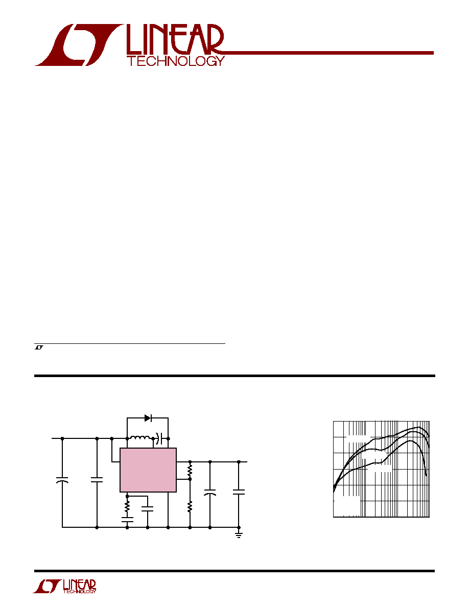
TYPICAL APPLICATIO
N
U
APPLICATIO S
U
DESCRIPTIO
U
FEATURES
Synchronous, Fixed Frequency
Step-Up DC/DC Converter
s
Output Disconnected from Input During Shutdown
s
Output Voltage Remains Regulated
When V
IN
> V
OUT
s
Controlled Input Current During Start-Up
s
300kHz Current Mode PWM Operation
s
Can Be Externally Synchronized
s
Internal 2A Switches
s
Operates with V
IN
as Low as 1.8V
s
Automatic Burst Mode Operation at Light Loads
s
Quiescent Current: 160
µ
A
s
Shutdown Current: 9
µ
A Typ
The LT
®
1306 is a fully integrated, fixed frequency syn-
chronous boost converter capable of generating 5V at 1A
from a Li-Ion cell. The device contains both the main
power switch and synchronous rectifier on chip and
automatically disconnects the output from the input in
shutdown, eliminating the need for external load discon-
nect circuitry. Additionally, the output remains regulated
when V
IN
exceeds V
OUT
, allowing difficult step-up/step-
down converter functions to be easily realized using a
single inductor.
The internal 300kHz oscillator of the LT1306 can be easily
synchronized to an external clock from 425kHz to 500kHz.
This allows switching harmonics to be tightly controlled
and eliminates any beat frequencies that may result from
a multifrequency system. The LT1306 automatically shifts
into power saving Burst Mode
TM
operation at light loads.
At heavy loads the LT1306 operates in fixed frequency
current mode. No-load quiescent current is 160
µ
A and
reduces to 9
µ
A in shutdown mode.
The LT1306 is available in an SO-8 package.
, LTC and LT are registered trademarks of Linear Technology Corporation.
Burst Mode is a trademark of Linear Technology Corporation.
s
Satellite Phones
s
Portable Instruments
s
Personal Digital Assistants
s
Palmtop Computers
LOAD CURRENT (mA)
1
60
EFFICIENCY (%)
80
85
90
10
100
1000
1306 TA01
75
70
65
V
IN
= 4.2V
V
IN
= 3.6V
V
IN
= 2.6V
V
O
= 5V
L1 = 10
µ
H
(FIGURE 1)
SW
L1
10
µ
H
D1
C1
1
µ
F
V
IN
CAP
LT1306
R3
118k
R2
249k
R1
768k
C
Z
68nF
C
IN2
0.1
µ
F
C
IN1
22
µ
F
1-CELL
Li-Ion
C
P
68pF
C
O2
1
µ
F
C
O1
220
µ
F
C
IN1
: AVX TAJC226M010
C
O1
: AVX TPSE227M010R0100
C
IN1
, C
O2
: CERAMIC
C1: AVX TAJA105K020
D1: MMBD914LT1
L1: CTX10-2
1306 F01
5V
1A
OUT
S/S
FB
V
C
GND
+
+
+
Efficiency
Figure 1. Single Li-Ion Cell to 5V Converter
2
LT1306
PARAMETER
CONDITIONS
MIN
TYP
MAX
UNITS
Reference Voltage
Measured at the FB Pin
q
1.22
1.24
1.26
V
Reference Line Regulation
1.8V
V
IN
7V
0.002
0.1
%/V
FB Input Bias Current
V
FB
= V
REF
q
10
25
nA
Error Amplifier Transconductance
I =
±
0.2
µ
A
80
150
220
µ
1
Error Amplifier Output Source Current
V
FB
= 1V, V
C
= 0.8V
5
7.5
11
µ
A
Error Amplifier Output Sink Current
V
FB
= 1.5V, V
C
= 0.8V
5
7.5
11
µ
A
Error Amplifier Output Clamp Voltage
V
FB
= 1V
1.18
1.28
1.38
V
V
IN
Undervoltage Lockout Threshold
1.55
1.8
V
Idle Mode Output Leakage Current
V
FB
= 1.5V, V
OUT
= 5.5V, V
SW
= 1.7V
q
6
15
µ
A
Output Source Current in Shutdown
V
OUT
= 0V, V
IN
= V
SW
= 7V, V
CAP
= 7.2V, V
S/S
= 0V
q
3
µ
A
Switching Frequency
1.8V
V
IN
7V, 0
°
C
T
A
85
°
C
q
260
310
415
kHz
1.8V
V
IN
7V, T
A
= 40
°
C
225
305
390
kHz
Maximum Duty Cycle
V
FB
= 1V, 0
°
C
T
A
85
°
C
80
90
%
V
FB
= 1V, T
A
= 40
°
C
65
80
%
Switch Current Limit
Duty Cycle = 0.1 (Note 3)
2.3
A
Duty Cycle = 0.8 (Note 3)
2.0
A
Burst Mode Operation Switch Current Limit
250
mA
Switch V
CESAT
I
SW
= 2A
0.45
0.575
V
Rectifier V
CESAT
I
SW
= 2A
0.49
0.675
V
Stepdown Mode Rectifier Voltage
V
OUT
= 0V, I
SW
= 1A
0.3 + V
IN
0.7 + V
IN
V
V
OUT
= 2.2V, I
SW
= 1A
1.3
1.8
V
Switch and Rectifier Leakage Current
V
OUT
= 0V, V
IN
= V
SW
= 7V, V
CAP
= 7.2V, V
S/S
= 0V
q
0.1
20
µ
A
ABSOLUTE
M
AXI
M
U
M
RATINGS
W
W
W
U
PACKAGE/ORDER I
N
FOR
M
ATIO
N
W
U
U
ORDER PART
NUMBER
(Note 1)
V
IN
Voltage ............................................................. 10V
S/S Voltage ............................................................... 7V
FB Voltage .............................................................. 10V
V
OUT
Voltage .......................................................... 5.5V
Junction Temperature .......................................... 125
°
C
Operating Temperature Range (Note 2) .. 40
°
C to 85
°
C
Storage Temperature Range ................. 65
°
C to 150
°
C
Lead Temperature (Soldering, 10 sec).................. 300
°
C
Consult factory for Industrial and Military grade parts.
S8 PART MARKING
LT1306ES8
1306
T
JMAX
= 125
°
C,
JA
= 90
°
C/ W
1
2
3
4
8
7
6
5
TOP VIEW
S8 PACKAGE
8-LEAD PLASTIC SO
V
C
FB
V
OUT
GND
S/S
V
IN
CAP
SW
ELECTRICAL CHARACTERISTICS
The
q
denotes the specifications which apply over the full operating
temperature range, otherwise specifications are at T
A
= 25
°
C. V
IN
= 2.5V, V
S/S
= V
IN
, V
C
open unless otherwise noted.
3
LT1306
PARAMETER
CONDITIONS
MIN
TYP
MAX
UNITS
S/S Pin Current
V
S/S
= V
IN
6
µ
A
V
S/S
= 0V
3
µ
A
Shutdown Pin Input High Voltage
1.2
V
Shutdown Pin Input Low Voltage
0.45
V
Shutdown Delay
12
20
50
µ
s
Synchronization Frequency Range
425
500
kHz
Operating Supply Current
4.5
8
mA
Quiescent Supply Current
V
S/S
= V
IN
, V
FB
= 1.5V
q
160
250
µ
A
Shutdown Supply Current
V
S/S
= 0V
9
16
µ
A
CAP Pin Leakage Current
V
IN
= V
CAP
= 7V, V
S/S
= 2.5V, I
SW
= 0
q
10
µ
A
Output Boost-to-Stepdown Threshold
V
IN
V
Output Stepdown-to-Boost Threshold
V
IN
0.1
V
The
q
denotes the specifications which apply over the full operating
temperature range, otherwise specifications are at T
A
= 25
°
C. V
IN
= 2.5V, V
S/S
= V
IN
, V
C
open unless otherwise noted.
ELECTRICAL CHARACTERISTICS
Note 1: Absolute Maximum Ratings are those values beyond which the life
to the device may be impaired.
Note 2: The LT1306E is guaranteed to meet performance specifications
from 0
°
C to 70
°
C. Specifications over the 40
°
C to 85
°
C operating
temperature range are assured by design, characterization and correlation
with statistical process controls.
Note 3: Switch current limit guaranteed by design/correlation to static
tests.
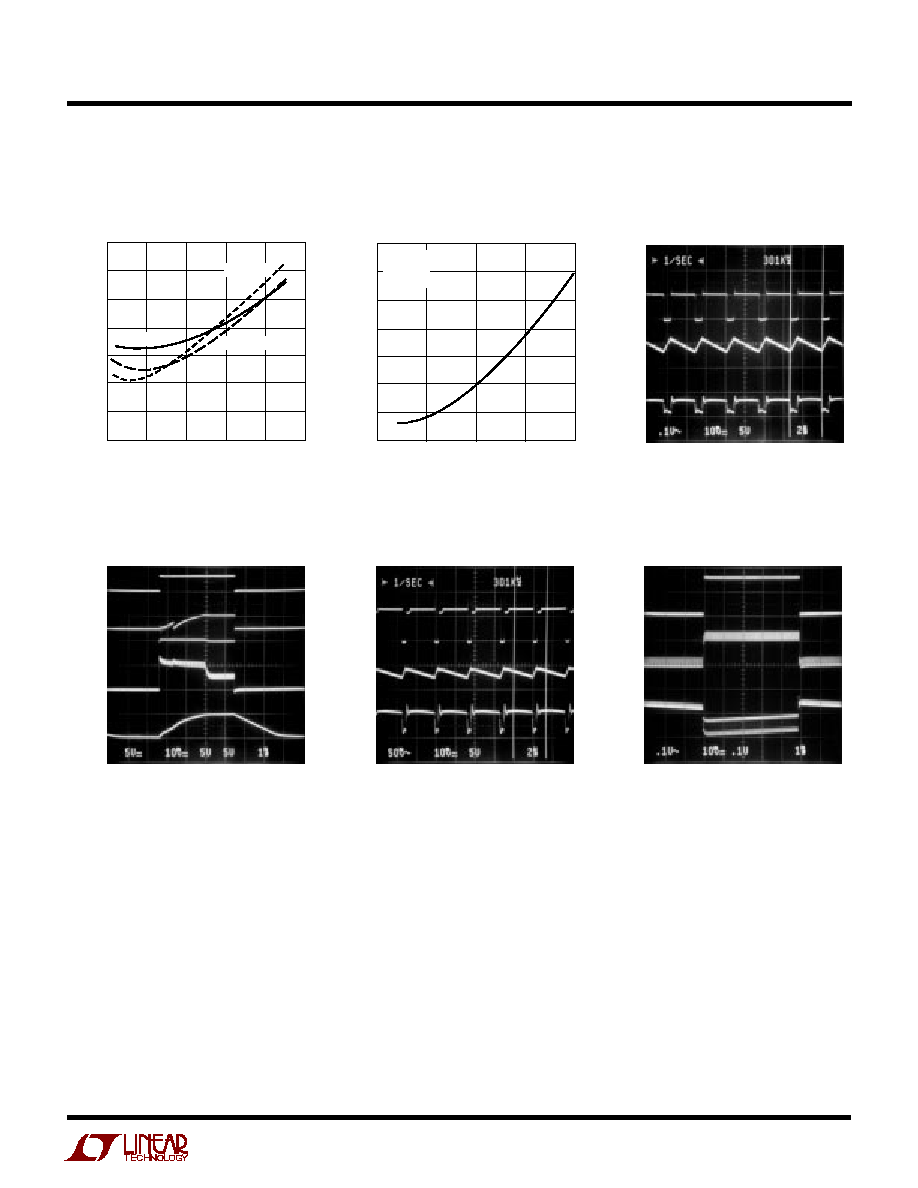
TYPICAL PERFOR
M
A
N
CE CHARACTERISTICS
U
W
V
IN
(V)
1.5 2.0 2.5 3.0 3.5 4.0 4.5 5.0 5.5 6.0 6.5 7.0
I
LOADMAX
(A)
1.0
1.5
1306 · G01
0.5
0
V
O
= 5V
L = 10
µ
H
T
J
= 125
°
C
T
A
= 25
°
C
T
A
= 50
°
C
V
O
= 3.3V
TEMPERATURE (
°
C)
40
REFERENCE VOLTAGE (V)
80
1306 · G02
0
40
1.239
1.238
1.237
1.236
1.235
1.234
1.233
1.232
1.231
20
20
60
100
V
S/S
(V)
5
4
3
2
1
0
1
2
3
4
5
I
S/S
(
µ
A)
1306 · G03
0
5
4
3
2
1
TA = 40
°
C
TA = 85
°
C
TA = 25
°
C
Maximum Load Current vs
Input Voltage
Reference Voltage vs
Temperature
S/S Pin Current vs S/S Pin Voltage
4
LT1306
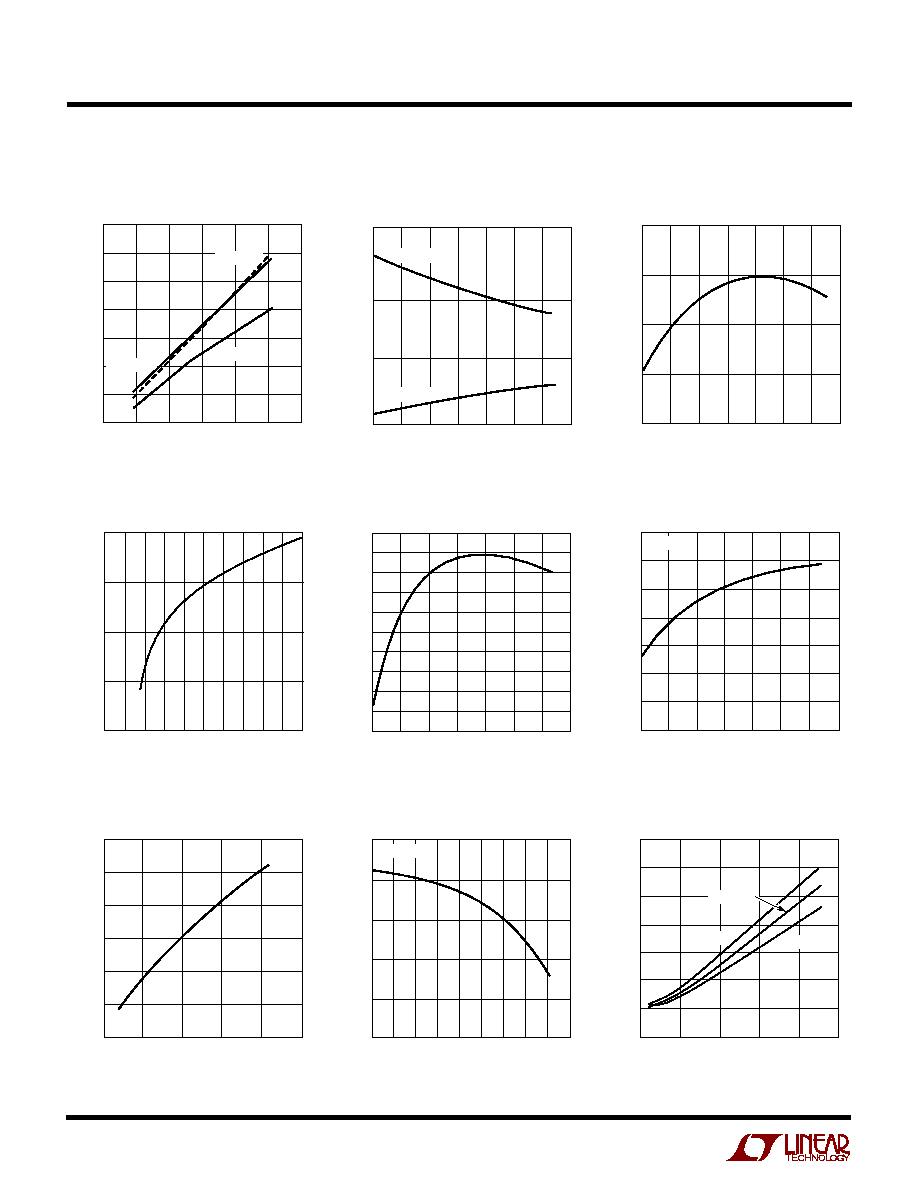
TYPICAL PERFOR
M
A
N
CE CHARACTERISTICS
U
W
S/S Pin Current vs Temperature
Shutdown Supply Current vs
Input Voltage
Idle-Mode Supply Current vs
Temperature
Oscillator Frequency Line
Regulation
Frequency vs Temperature
Maximum Duty Ratio
V
IN
(V)
0
FREQUENCY (kHz)
9
8
7
6
1306 · G07
2
4
320
315
310
305
300
1
3
5
10
TEMPERATURE (
°
C)
40
FREQUENCY (kHz)
315
310
305
300
295
290
285
280
275
270
265
0
40
60
1306 · G08
20
20
80
100
TEMPERATURE (
°
C)
40
95
90
85
80
75
70
65
60
20
60
1306 · G09
20
0
40
80
100
DUTY RATIO (%)
V
IN
= 2.5V
Current Limit vs Duty Cycle
Switch Saturation Voltage
vs Current
Maximum Allowable Rise Time of
Synchronizing Pulse
SYNCHRONIZING PULSE AMPLITUDE (V)
1
MAXIMUM RISE TIME (ns)
600
500
400
300
200
100
0
1.5
2.0
2.5
3.0
1306 · G10
3.5
DUTY CYCLE (%)
0
2.0
CURRENT LIMIT (A)
2.2
2.6
2.8
3.0
20
40
50
90
1306 · G11
2.4
10
30
60
70
80
T
A
= 25
°
C
SWITCH CURRENT (A)
0
0.7
0.6
0.5
0.4
0.3
0.2
0.1
0
1.5
1306 · G12
0.5
1.0
2.0
2.5
SWITCH VOLTAGE (V)
TA = 40
°
C
TA = 85
°
C
TA = 25
°
C
INPUT VOLTAGE (V)
SUPPLY CURRENT (
µ
A)
40
35
30
25
20
15
10
5
1306 · G04
0
2
4
6
8
10
12
TA = 85
°
C
TA = 25
°
C
TA = 40
°
C
TEMPERATURE (
°
C)
40
IDLE-MODE SUPPLY CURRENT (
µ
A)
80
1306 · G06
0
40
155
150
145
140
135
20
20
60
100
TEMPERATURE (
°
C)
S/S CURRENT (
µ
A)
5.0
2.5
0
2.5
1306 · G05
40
20
0
20
40
80
60
100
V
S/S
= 2.5V
V
S/S
= 0V
5
LT1306
TYPICAL PERFOR
M
A
N
CE CHARACTERISTICS
U
W
RECTIFIER CURRENT (A)
0
0.7
0.6
0.5
0.4
0.3
0.2
0.1
0
1.5
1306 · G13
0.5
1.0
2.0
2.5
RECTIFIER VOLTAGE (V)
TA = 40
°
C
TA = 25
°
C
TA = 85
°
C
RECTIFIER CURRENT (A)
0
1.90
1.85
1.80
1.75
1.70
1.65
1.60
1.55
1.5
1306 · G14
0.5
1.0
2.0
RECTIFIER VOLTAGE (V)
V
IN
= 6V
V
OUT
= 5V
T
A
= 25
°
C
Rectifier Saturation Voltage
vs Current
Stepdown-Mode Rectifier Voltage
vs Current
Continuous-Conduction Mode
Switching Waveforms in Boost
Operation
V
O
0.1V/DIV
AC
V
SW
5V/DIV
I
L
0.5A/DIV
V
IN
= 4.2V
V
O
= 5V
2
µ
s/DIV
1ms/DIV
2
µ
s/DIV
1ms/DIV
V
IN
= 2.5V
V
O
5V/DIV
V
SW
5V/DIV
I
L
2A/DIV
V
S/S
5V/DIV
Start-Up to Shutdown Transient
Response*
Continuous-Conduction Mode
Switching Waveforms in
Stepdown Mode
V
IN
= 6V
V
O
= 5V
V
O
50mV/DIV
AC
V
SW
5V/DIV
I
L
0.5V/DIV
Transient Response of the
Converter in Figure 1 with a
50mA to 800mA Load Step
V
IN
= 3.6V
V
O
= 5V
LOAD
CURRENT
0.5A/DIV
DC
INDUCTOR
CURRENT
1A/DIV
OUTPUT
0.1V/DIV
AC
*Notice that the Input Start-Up Current is well Controlled and the
Output Voltage Falls to Zero in Shutdown.