 | ÐлекÑÑоннÑй компоненÑ: LT1513I | СкаÑаÑÑ:  PDF PDF  ZIP ZIP |
Äîêóìåíòàöèÿ è îïèñàíèÿ www.docs.chipfind.ru
1
LT1513/LT1513-2
SEPIC Constant- or
Programmable-Current/
Constant-Voltage Battery Charger
The LT
®
1513 is a 500kHz current mode switching regula-
tor specially configured to create a constant- or program-
mable-current/constant-voltage battery charger. In addition
to the usual voltage feedback node, it has a current sense
feedback circuit for accurately controlling output current
of a flyback or SEPIC (Single-Ended Primary Inductance
Converter) topology charger. These topologies allow the
current sense circuit to be ground referred and completely
separated from the battery itself, simplifying battery switch-
ing and system grounding problems. In addition, these
topologies allow charging even when the input voltage is
lower than the battery voltage. The LT1513 can also drive
a CCFL Royer converter with high efficiency in floating or
grounded mode.
Maximum switch current on the LT1513 is 3A. This allows
battery charging currents up to 2A for a single lithium-ion
cell. Accuracy of 1% in constant-voltage mode is perfect
for lithium battery applications. Charging current can be
easily programmed for all battery types.
DESCRIPTIO
N
U
s
Charger Input Voltage May Be Higher, Equal to or
Lower Than Battery Voltage
s
Charges Any Number of Cells Up to 20V
s
1% Voltage Accuracy for Rechargeable Lithium
Batteries
s
100mV Current Sense Voltage for High Efficiency
(LT1513)
s
0mV Current Sense Voltage for Easy Current
Programming (LT1513-2)
s
Battery Can Be Directly Grounded
s
500kHz Switching Frequency Minimizes
Inductor Size
s
Charging Current Easily Programmable or Shut Down
FEATURES
INPUT VOLTAGE (V)
0
5
CURRENT (A)
2.4
2.2
2.0
1.8
1.6
1.4
1.2
1.0
0.8
0.6
0.4
25
LT1513 · TA02
10
15
20
30
12V
INDUCTOR = 10
µ
H
ACTUAL PROGRAMMED CHARGING CURRENT WILL BE
INDEPENDENT OF INPUT VOLTAGE IF IT DOES NOT
EXCEED VALUES SHOWN
SINGLE Li-Ion CELL
(4.1V)
DOUBLE Li-Ion
CELL (8.2V)
16V
20V
BATTERY
VOLTAGE
Maximum Charging Current
, LTC and LT are registered trademarks of Linear Technology Corporation.
s
Charging of NiCd, NiMH, Lead-Acid or Lithium
Rechargeable Cells
s
Precision Current Limited Power Supply
s
Constant-Voltage/Constant-Current Supply
s
Transducer Excitation
s
Universal Input CCFL Driver
APPLICATIO
N
S
U
Figure 1. SEPIC Charger with 1.25A Output Current
LT1513
I
FB
V
C
V
IN
L1A*
L1B*
1.25A
1
3
2
5
7
·
·
6
TAB
4
GND
V
FB
LT1513 · TA01
V
SW
SYNC
AND/OR
SHUTDOWN
WALL
ADAPTER
INPUT
S/S
C3
22
µ
F
25V
C2**
4.7
µ
F
C5
0.1
µ
F
*
**
L1A, L1B ARE TWO 10
µ
H WINDINGS ON A
COMMON CORE: COILTRONICS CTX10-4
CERAMIC MARCON THCR40EIE475Z OR TOKIN 1E475ZY5U-C304
MBRD340 OR MBRS340T3. MBRD340 HAS 5
µ
A TYPICAL
LEAKAGE, MBRS340T3 50
µ
A TYPICAL
C4
0.22
µ
F
R4
39
R1
R2
R5
270
R3
0.08
C1
22
µ
F
25V
×
2
D1
CHARGE
SHUTDOWN
+
+
TYPICAL APPLICATIO
N
U
2
LT1513/LT1513-2
A
U
G
W
A
W
U
W
A
R
BSOLUTE
XI
TI
S
Supply Voltage ....................................................... 30V
Switch Voltage ........................................................ 40V
S/S Pin Voltage ....................................................... 30V
FB Pin Voltage (Transient, 10ms) .........................
±
10V
V
FB
Pin Current .................................................... 10mA
I
FB
Pin Voltage (Transient, 10ms) .........................
±
10V
Operating Junction Temperature Range
LT1513C ............................................... 0
°
C to 125
°
C
LT1513I ............................................ 40
°
C to 125
°
C
Short Circuit ......................................... 0
°
C to 150
°
C
Storage Temperature Range ................ 65
°
C to 150
°
C
Lead Temperature (Soldering, 10 sec) ................. 300
°
C
ELECTRICAL C
C
HARA TERISTICS
V
IN
= 5V, V
C
= 0.6V, V
FB
= V
REF
, I
FB
= 0V, V
SW
and S/S pins open, unless otherwise noted.
SYMBOL
PARAMETER
CONDITIONS
MIN
TYP
MAX
UNITS
V
REF
FB Reference Voltage
Measured at FB Pin
1.233
1.245
1.257
V
V
C
= 0.8V
q
1.228
1.245
1.262
V
FB Input Current
V
FB
= V
REF
300
550
nA
q
600
nA
FB Reference Voltage Line Regulation
2.7V
V
IN
25V, V
C
= 0.8V
q
0.01
0.03
%/V
V
IREF
I
FB
Reference Voltage (LT1513)
Measured at I
FB
Pin
107
100
93
mV
V
FB
= 0V, V
C
= 0.8V
q
110
100
90
mV
I
FB
Input Current
V
IFB
= V
IREF
(Note 2)
q
10
25
35
µ
A
I
FB
Reference Voltage Line Regulation
2.7V
V
IN
25V, V
C
= 0.8V
q
0.01
0.05
%/V
I
FBVOS
I
FB
Voltage Offset (LT1513-2) (Note 3)
I
VFB
= 60
µ
A (Note 4)
q
7.5
2.5
12.5
mV
I
FB
Input Current
V
IFB
= V
IREF
q
200
10
0
nA
V
FB
Source Current
V
IREF
= 10mV, V
FB
= 1.2V
q
700
300
100
µ
A
g
m
Error Amplifier Transconductance
I
C
=
±
25
µ
A
1100
1500
1900
µ
mho
q
700
2300
µ
mho
Error Amplifier Source Current
V
FB
= V
REF
150mV, V
C
= 1.5V
q
120
200
350
µ
A
Error Amplifier Sink Current
V
FB
= V
REF
+ 150mV, V
C
= 1.5V
q
1400
2400
µ
A
W
U
U
PACKAGE/ORDER I FOR ATIO
Consult factory for Military grade parts.
ORDER PART
NUMBER
LT1513CR
LT1513CR-2
LT1513IR
LT1513IR-2
T
JMAX
= 125
°
C,
JA
= 30
°
C/ W
WITH PACKAGE SOLDERED TO 0.5INCH
2
COPPER
AREA OVER BACKSIDE GROUND PLANE OR INTERNAL
POWER PLANE,
JA
CAN VARY FROM 20
°
C/W TO
> 40
°
C/W DEPENDING ON MOUNTING TECHNIQUE
R PACKAGE
7-LEAD PLASTIC DD
FRONT VIEW
TAB
IS
GND
V
IN
S/S
V
SW
GND
I
FB
FB
V
C
7
6
5
4
3
2
1
ORDER PART
NUMBER
LT1513CT7-2
LT1513IT7-2
T
JMAX
= 125
°
C,
JA
= 50
°
C/ W,
JC
= 4
°
C/W
T7 PACKAGE
7-LEAD TO-220
V
IN
S/S
V
SW
GND
I
FB
FB
V
C
FRONT VIEW
7
6
5
4
3
2
1
3
LT1513/LT1513-2
ELECTRICAL C
C
HARA TERISTICS
V
IN
= 5V, V
C
= 0.6V, V
FB
= V
REF
, I
FB
= 0V, V
SW
and S/S pins open, unless otherwise noted.
SYMBOL
PARAMETER
CONDITIONS
MIN
TYP
MAX
UNITS
Error Amplifier Clamp Voltage
High Clamp, V
FB
= 1V
1.70
1.95
2.30
V
Low Clamp, V
FB
= 1.5V
0.25
0.40
0.52
V
A
V
Error Amplifier Voltage Gain
500
V/ V
V
C
Pin Threshold
Duty Cycle = 0%
0.8
1
1.25
V
f
Switching Frequency
2.7V
V
IN
25V
450
500
550
kHz
0
°
C
T
J
125
°
C
430
500
580
kHz
T
J
< 0
°
C
400
580
kHz
Maximum Switch Duty Cycle
q
85
95
%
Switch Current Limit Blanking Time
130
260
ns
BV
Output Switch Breakdown Voltage
0
°
C
T
J
125
°
C
40
47
V
T
J
< 0
°
C
35
V
V
SAT
Output Switch ON Resistance
I
SW
= 2A
q
0.25
0.45
I
LIM
Switch Current Limit
Duty Cycle = 50%
q
3.0
3.8
5.4
A
Duty Cycle = 80% (Note 1)
q
2.6
3.4
5.0
A
I
IN
/
I
SW
Supply Current Increase During Switch ON Time
15
25
mA/A
Control Voltage to Switch Current
4
A/V
Transconductance
Minimum Input Voltage
q
2.4
2.7
V
I
Q
Supply Current
2.7V
V
IN
25V
q
4
5.5
mA
Shutdown Supply Current
2.7V
V
IN
25V, V
S/S
0.6V, T
J
0
°
C
q
12
30
µ
A
T
J
< 0
°
C
50
µ
A
Shutdown Threshold
2.7V
V
IN
25V
q
0.6
1.3
2
V
Shutdown Delay
q
5
12
25
µ
s
S/S Pin Input Current
0V
V
S/S
5V
q
10
15
µ
A
Synchronization Frequency Range
q
600
800
kHz
The
q
denotes specifications which apply over the full operating
temperature range.
Note 1: For duty cycles (DC) between 50% and 85%, minimum
guaranteed switch current is given by I
LIM
= 1.33 (2.75 DC).
Note 2: The I
FB
pin is servoed to its regulating state with V
C
= 0.8V.
Note 3: Consult factory for grade selected parts.
Note 4: The I
FB
pin is sevoed to regulate FB to 1.245V
4
LT1513/LT1513-2
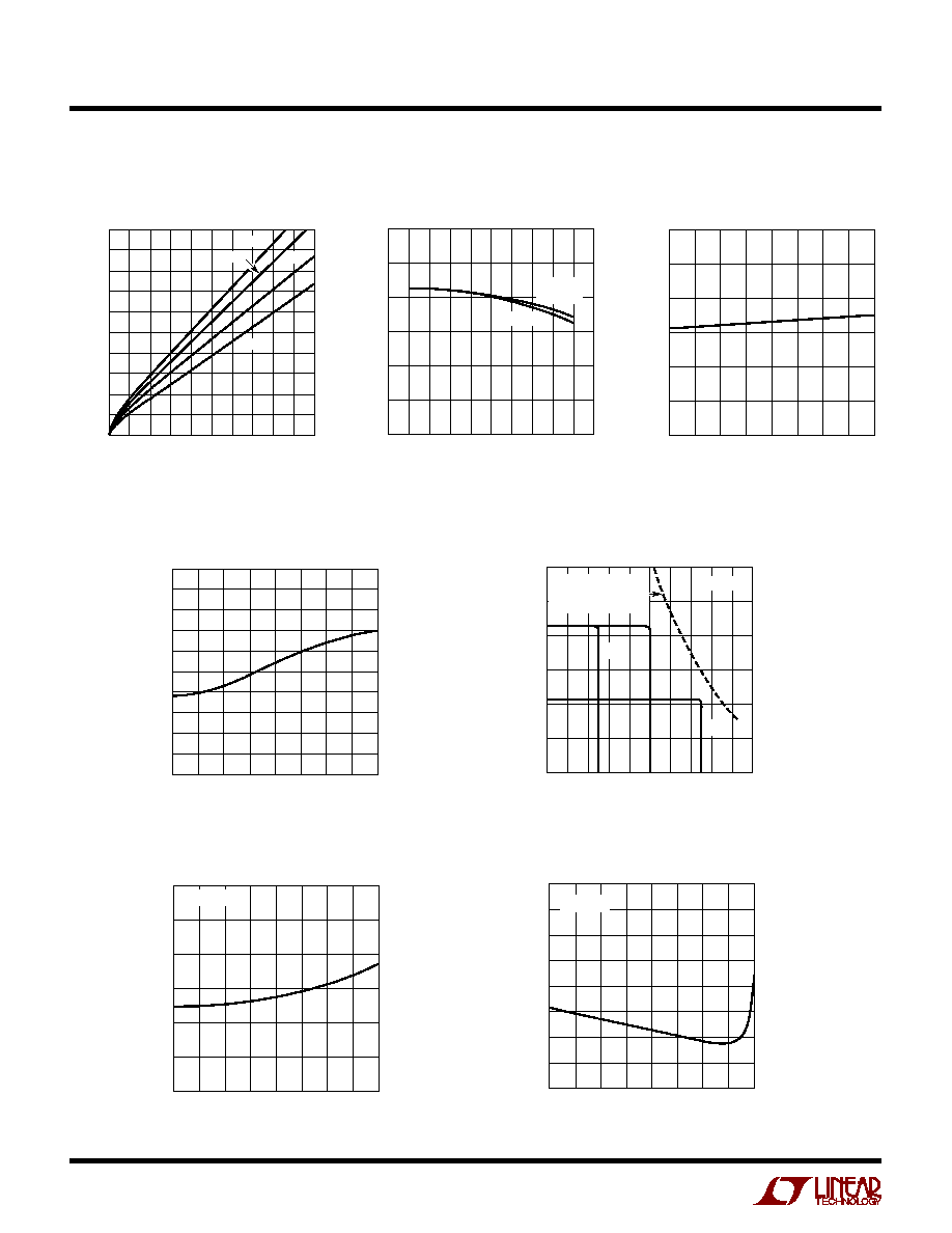
TEMPERATURE (
°
C)
50
50
NEGATIVE FEEDBACK INPUT CURRENT (
µ
A)
30
0
0
50
75
LT1513 · G06
40
10
20
25
25
100 125
150
CHARGING CURRENT (A)
BATTERY VOLTAGE (V)
12
10
8
6
4
2
0
0.4
0.8
1.2
1.6
1513 G07
2.0
0.2
0
0.6
1.0
1.4
1.8
(A) 8.4V BATTERY
I
CHRG
= 0.5A
(B) 8.4V BATTERY
I
CHRG
= 1A
(C) 4.2V BATTERY
I
CHRG
= 1.5A
V
IN
= 12V
MAXIMUM AVAILABLE
CHARGING CURRENT
WITH 12V INPUT
(A)
(B)
(C)
Negative Feedback Input Current
vs Temperature
Output Charging Characteristics
Showing Constant-Current and
Constant-Voltage Operation
TEMPERATURE (
°
C)
50
0
MINIMUM SYNCHRONIZATION VOLTAGE (V
P-P
)
0.5
1.0
1.5
2.0
0
50
100
150
LT1513 · G04
2.5
3.0
25
25
75
125
f
SYNC
= 700kHz
Minimum Peak-to-Peak
Synchronization Voltage vs Temperature
TEMPERATURE (
°
C)
50
FEEDBACK INPUT CURRENT (nA)
400
500
600
150
LT1513 · G05
300
200
0
0
50
100
100
800
700
25
25
75
125
V
FB
= V
REF
Feedback Input Current
vs Temperature
TYPICAL PERFOR
M
A
N
CE CHARACTERISTICS
U
W
Switch Saturation Voltage
vs Switch Current
Minimum Input Voltage
vs Temperature
Switch Current Limit
vs Duty Cycle
TEMPERATURE (
°
C)
50
1.8
INPUT VOLTAGE (V)
2.0
2.2
2.4
2.6
0
50
100
150
LT1513 · G03
2.8
3.0
25
25
75
125
DUTY CYCLE (%)
0
SWITCH CURRENT LIMIT (A)
2
4
6
1
3
5
20
40
60
80
LT1513 · G02
100
10
0
30
50
70
90
25
°
C AND
125
°
C
55
°
C
SWITCH CURRENT (A)
0
SWITCH SATURATION VOLTAGE (V)
0.6
0.8
1.0
3.2
LT1513 · G01
0.4
0.2
0.5
0.7
0.9
0.3
0.1
0
0.8
1.6
2.4
4.0
2.8
0.4
1.2
2.0
3.6
100
°
C
150
°
C
25
°
C
55
°
C

5
LT1513/LT1513-2
PI
N
FU
N
CTIO
N
S
U
U
U
V
C
(Pin 1): The compensation pin is primarily used for
frequency compensation, but it can also be used for soft
starting and current limiting. It is the output of the error
amplifier and the input of the current comparator. Peak
switch current increases from 0A to 3.6A as the V
C
voltage
varies from 1V to 1.9V. Current out of the V
C
pin is about
200
µ
A when the pin is externally clamped below the
internal 1.9V clamp level. Loop frequency compensation
is performed with a capacitor or series RC network from
the V
C
pin
directly to the ground pin (avoid ground loops).
FB (Pin 2): The feedback pin is used for positive output
voltage sensing. The R1/R2 voltage divider connected to
FB defines Li-Ion float voltage at full charge, or acts as a
voltage limiter for NiCd or NiMH applications. FB is the
inverting input to the voltage error amplifier. Input bias
current is typically 300nA, so divider current is normally
set to 100
µ
A to swamp out any output voltage errors due
to bias current. The noninverting input of this amplifier is
tied internally to a 1.245V reference. The grounded end of
the output voltage divider should be connected directly to
the LT1513 ground pin (avoid ground loops).
I
FB
(Pin 3): The current feedback pin is used to sense
charging current. It is the input to a current sense amplifier
that controls charging current when the battery voltage is
below a programmed limit. During constant-current
operation, the LT1513 I
FB
pin regulates at 100mV. Input
resistance of this pin is 5k
, so filter resistance (R4,
Figure 1) should be less than 50
. The 39
, 0.22
µ
F filter
shown in Figure 1 is used to convert the pulsating current
in the sense resistor to a smooth DC current feedback
signal. The LT1513-2 I
FB
pin regulates at 0mV to provide
programmable current limit. The current through R5,
Figure 5, is balanced by the current through R4, program-
ming the maximum voltage across R3.
GND (Pin 4): The ground pin is common to both control
circuitry and switch current. V
C
, FB and S/S signals must
be Kelvin and connected as close as possible to this pin.
The TAB of the R package should also be connected to the
power ground.
V
SW
(Pin 5): The switch pin is the collector of the power
switch, carrying up to 3A of current with fast rise and fall
times. Keep the traces on this pin as short as possible to
minimize radiation and voltage spikes. In particular, the
path in Figure 1 which includes SW to C2, D1, C1 and
around to the LT1513 ground pin should be as short as
possible to minimize voltage spikes at switch turn-off.
S/S (Pin 6): This pin can be used for shutdown and/or
synchronization. It is logic level compatible, but can be
tied to V
IN
if desired. It defaults to a high ON state when
floated. A logic low state will shut down the charger to a
micropower state. Driving the S/S pin with a continuous
logic signal of 600kHz to 800kHz will synchronize switch-
ing frequency to the external signal. Shutdown is avoided
in this mode with an internal timer.
V
IN
(Pin 7): The input supply pin should be bypassed with
a low ESR capacitor located right next to the IC chip. The
grounded end of the capacitor must be connected directly
to the ground plane to which the TAB is connected.
TAB: The TAB on the surface mount R package is electri-
cally connected to the ground pin, but a low inductance
connection must be made to both the TAB and the pin for
proper circuit operation. See suggested PC layout in
Figure 4.