 | –≠–ª–µ–∫—Ç—Ä–æ–Ω–Ω—ã–π –∫–æ–º–ø–æ–Ω–µ–Ω—Ç: LT1713 | –°–∫–∞—á–∞—Ç—å:  PDF PDF  ZIP ZIP |

1
LT1715
s
UltraFast: 4ns at 20mV Overdrive
s
150MHz Toggle Frequency
s
Separate Input and Output Power Supplies
s
Low Power: 4.6mA per Comparator at 3V
s
Pinout Optimized for High Speed Use
s
Output Optimized for 3V and 5V Supplies
s
TTL/CMOS Compatible Rail-to-Rail Output
s
Input Voltage Range Extends 100mV
Below Negative Rail
s
Internal Hysteresis with Specified Limits
The LT
Æ
1715 is an UltraFast
TM
dual comparator optimized
for low voltage operation. Separate supplies allow inde-
pendent analog input ranges and output logic levels with
no loss of performance. The input voltage range extends
from 100mV below V
EE
to 1.2V below V
CC
. Internal hyster-
esis makes the LT1715 easy to use even with slow moving
input signals. The rail-to-rail outputs directly interface to
TTL and CMOS. The symmetric output drive results in
similar rise and fall times that can be harnessed for analog
applications or for easy translation to other single supply
logic levels.
The LT1715 is available in the 10-pin MSOP package. The
pinout of the LT1715 minimizes parasitic effects by plac-
ing the most sensitive inputs away from the outputs,
shielded by the power rails.
For a dual/quad single supply comparator with similar
propagation delay, see the LT1720/LT1721. For a single
comparator with similar propagation delay, see the LT1719.
s
High Speed Differential Line Receivers
s
Level Translators
s
Window Comparators
s
Crystal Oscillator Circuits
s
Threshold Detectors/Discriminators
s
High Speed Sampling Circuits
s
Delay Lines
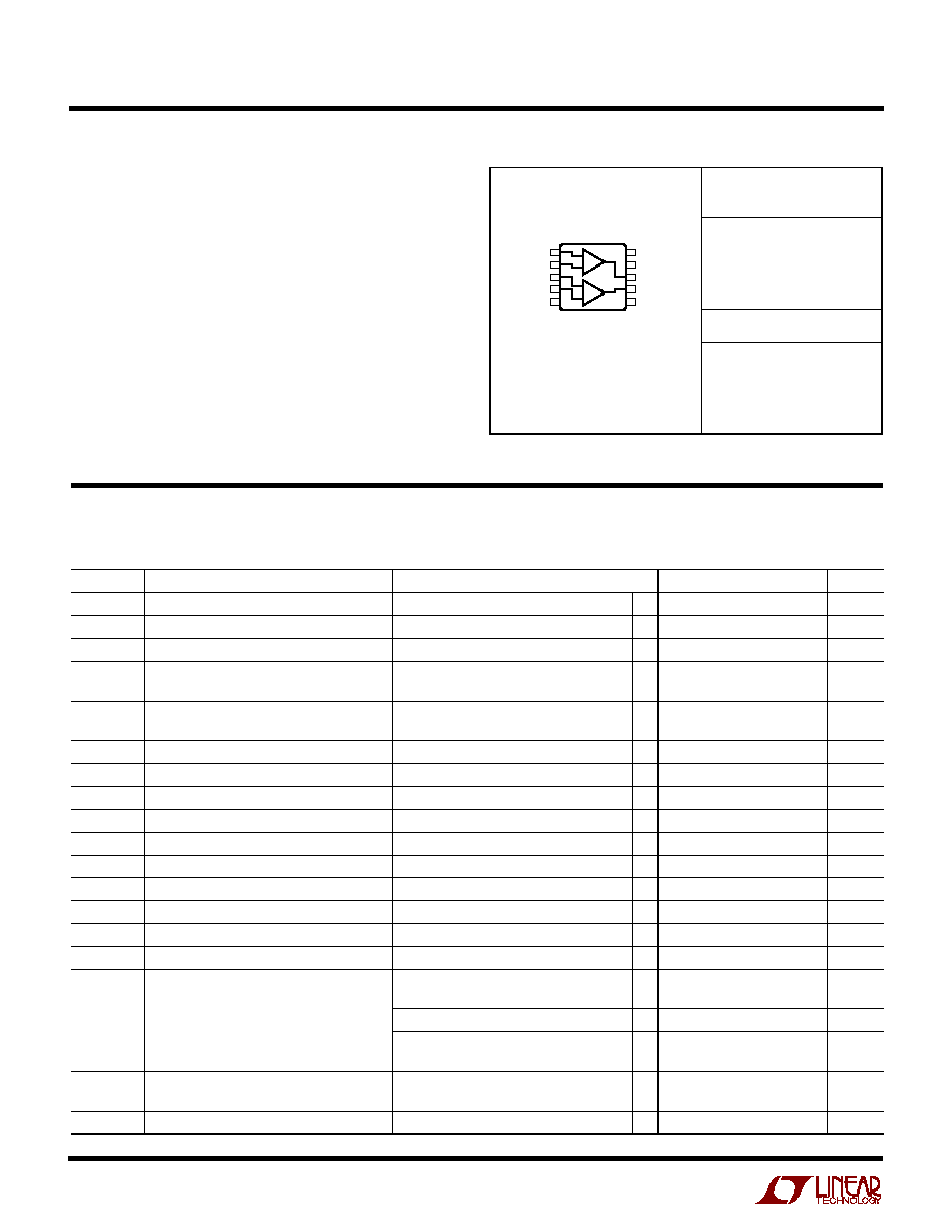
100MHz Dual Differential Line Receiver
Line Receiver Response to 100MHz Clock,
50MHz Data Both with 25mV
P-P
Inputs
4ns, 150MHz
Dual Comparator with
Independent Input/Output Supplies
, LTC and LT are registered trademarks of Linear Technology Corporation.
UltraFast is a trademark of Linear Technology Corporation.
≠
+
≠
+
1715 TA01
IN A
OUT A
OUT B
≠5V
5V
3V
IN B
FEATURES
DESCRIPTIO
U
APPLICATIO S
U
TYPICAL APPLICATIO
U
3V
CLOCK OUT
0V
3V
DATA OUT
0V
FET PROBES
5ns/DIV
1715 TA02
1V/DIV
1V/DIV
2
LT1715
ORDER PART
NUMBER
(Note 1)
Supply Voltage
+ V
S
to GND .......................................................... 7V
V
CC
to V
EE
........................................................ 13.2V
+ V
S
to V
EE
....................................................... 13.2V
V
EE
to GND ....................................... ≠ 13.2V to 0.3V
Input Current (+ IN, ≠ IN) ...................................
±
10mA
Output Current (Continuous) ............................
±
20mA
Operating Temperature Range ................ ≠ 40
∞
C to 85
∞
C
Specified Temperature Range (Note 2) ... ≠ 40
∞
C to 85
∞
C
Junction Temperature .......................................... 150
∞
C
Storage Temperature Range ................ ≠ 65
∞
C to 150
∞
C
Lead Temperature (Soldering, 10 sec)................. 300
∞
C
MS10 PART MARKING
LTVQ
LTVV
LT1715CMS
LT1715IMS
T
JMAX
= 150
∞
C,
JA
= 120
∞
C/ W (NOTE 3)
SYMBOL
PARAMETER
CONDITIONS
MIN
TYP
MAX
UNITS
V
CC
≠ V
EE
Input Supply Voltage
q
2.7
12
V
+ V
S
Output Supply Voltage
q
2.7
6
V
V
CMR
Input Voltage Range
(Note 4)
q
V
EE
≠ 0.1
V
CC
≠ 1.2
V
V
TRIP
+
Input Trip Points
(Note 5)
q
≠ 1.5
5.5
mV
V
TRIP
≠
q
≠ 5.5
1.5
mV
V
OS
Input Offset Voltage
(Note 5)
0.4
2.5
mV
q
3.5
mV
V
HYST
Input Hysteresis Voltage
(Note 5)
q
2
3.5
6
mV
V
OS
/
T
Input Offset Voltage Drift
q
10
µ
V/
∞
C
I
B
Input Bias Current
q
≠ 6
≠2.5
0
µ
A
I
OS
Input Offset Current
q
0.2
0.6
µ
A
CMRR
Common Mode Rejection Ratio
(Note 6)
q
60
70
dB
PSRR
Power Supply Rejection Ratio
(Note 7)
q
65
80
dB
A
V
Voltage Gain
(Note 8)
V
OH
Output High Voltage
I
SOURCE
= 4mA, V
IN
= V
TRIP
+
+ 20mV
q
+ V
S
≠ 0.4
V
V
OL
Output Low Voltage
I
SINK
= 10mA, V
IN
= V
TRIP
≠
≠ 20mV
q
0.4
V
f
MAX
Maximum Toggle Frequency
(Note 9)
150
MHz
t
PD20
Propagation Delay
V
OVERDRIVE
= 20mV (Note 10),
2.8
4
6
ns
V
CC
= 5V, V
EE
= ≠5V
q
2.8
7
ns
V
OVERDRIVE
= 20mV, V
CC
= 5V, V
EE
= 0V
4.4
ns
V
OVERDRIVE
= 20mV, V
CC
= 3V, V
EE
= 0V
3
4.8
6.5
ns
q
3
7.5
ns
t
PD5
Propagation Delay
V
OVERDRIVE
= 5mV, V
EE
= 0V (Notes 10, 11)
6
9
ns
q
12
ns
t
SKEW
Propagation Delay Skew
(Note 12) Between t
PD
+
/t
PD
≠
, V
EE
= 0V
q
0.5
1.5
ns
The
q
denotes specifications that apply over the full operating temperature
range, otherwise specifications are at T
A
= 25
∞
C. V
CC
= 5V, V
EE
= ≠5V, +V
S
= 5V, V
CM
= 1V, C
OUT
= 10pF, V
OVERDRIVE
= 20mV,
unless otherwise specified.
1
2
3
4
5
+IN A
≠IN A
≠IN B
+IN B
V
EE
10
9
8
7
6
V
CC
+V
S
OUT A
OUT B
GND
TOP VIEW
MS10 PACKAGE
10-LEAD PLASTIC MSOP
A
B
ABSOLUTE AXI U RATI GS
W
W
W
U
PACKAGE/ORDER I FOR ATIO
U
U
W
ELECTRICAL CHARACTERISTICS
Consult factory for parts specified with wider operating temperature ranges.
3
LT1715
SYMBOL
PARAMETER
CONDITIONS
MIN
TYP
MAX
UNITS
t
PD
Differential Propagation Delay
(Note 13) Between Channels
q
0.3
1
ns
t
r
Output Rise Time
10% to 90%
2
ns
t
f
Output Fall Time
90% to 10%
2
ns
t
JITTER
Output Timing Jitter
V
IN
= 1.2V
P-P
(6dBm), Z
IN
= 50
t
PD
+
15
ps
RMS
f = 20MHz (Note 14) t
PD
≠
11
ps
RMS
I
CC
Positive Input Stage Supply Current
+ V
S
= V
CC
= 5V, V
EE
= ≠ 5V
q
1
2
mA
(per Comparator)
+ V
S
= V
CC
= 3V, V
EE
= 0V
q
0.9
1.6
mA
I
EE
Negative Input Stage Supply Current
+ V
S
= V
CC
= 5V, V
EE
= ≠ 5V
q
≠ 4.8
≠ 2.9
mA
(per Comparator)
+ V
S
= V
CC
= 3V, V
EE
= 0V
q
≠ 3.8
≠ 2.4
mA
I
S
Positive Output Stage Supply Current
+ V
S
= V
CC
= 5V, V
EE
= ≠ 5V
q
4.6
7.5
mA
(per Comparator)
V
S
= V
CC
= 3V, V
EE
= 0V
q
3.7
6
mA
The
q
denotes specifications that apply over the full operating temperature
range, otherwise specifications are at T
A
= 25
∞
C. V
CC
= 5V, V
EE
= ≠5V, +V
S
= 5V, V
CM
= 1V, C
OUT
= 10pF, V
OVERDRIVE
= 20mV,
unless otherwise specified.
Note 1: Absolute Maximum Ratings are those values beyond which the life
of a device may be impaired.
Note 2: The LT1715C is guaranteed to meet specified performance from
0
∞
C to 70
∞
C. The LT1715C is designed, characterized and expected to
meet specified performance from ≠40
∞
C to 85
∞
C but is not tested or QA
sampled at these temperatures. The LT1715I is guaranteed to meet
specified performance from ≠40
∞
C to 85
∞
C.
Note 3: Thermal resistances vary depending upon the amount of PC board
metal attached to Pin 5 of the device.
JA
is specified for a 2500mm
2
3/32"
FR-4 board covered with 2oz copper on both sides and with 100mm
2
of
copper attached to Pin 5. Thermal performance can be improved beyond
the given specification by using a 4-layer board or by attaching more metal
area to Pin 5.
Note 4: If one input is within these common mode limits, the other input
can go outside the common mode limits and the output will be valid.
Note 5: The LT1715 comparator includes internal hysteresis. The trip
points are the input voltage needed to change the output state in each
direction. The offset voltage is defined as the average of V
TRIP
+
and V
TRIP
≠
,
while the hysteresis voltage is the difference of these two.
Note 6: The common mode rejection ratio is measured with V
CC
= 5V,
V
EE
= ≠ 5V and is defined as the change in offset voltage measured from
V
CM
= ≠ 5.1V to V
CM
= 3.8V, divided by 8.9V.
Note 7: The power supply rejection ratio is measured with V
CM
= 1V and is
defined as the worst of: the change in offset voltage from V
CC
= + V
S
=
2.7V to V
CC
= + V
S
= 6V (with V
EE
= 0V) divided by 3.3V or the change in
offset voltage from V
EE
= 0V to V
EE
= ≠ 6V (with V
CC
= +V
S
= 6V) divided
by 6V.
Note 8: Because of internal hysteresis, there is no small-signal region in
which to measure gain. Proper operation of internal circuity is ensured by
measuring V
OH
and V
OL
with only 20mV of overdrive.
Note 9: Maximum toggle rate is defined as the highest frequency at which
a 100mV sinusoidal input results in an error free output toggling to greater
than 4V when high and to less than 1V when low on a 5V output supply.
Note 10: Propagation delay measurements made with 100mV steps.
Overdrive is measured relative to V
TRIP
±
.
Note 11: t
PD
cannot be measured in automatic handling equipment with
low values of overdrive. The LT1715 is 100% tested with a 100mV step
and 20mV overdrive. Correlation tests have shown that t
PD
limits can be
guaranteed with this test.
Note 12: Propagation Delay Skew is defined as:
t
SKEW
= |t
PDLH
≠ t
PDHL
|
Note 13: Differential propagation delay is defined as the larger of the two:
t
PDLH
= |t
PDLHA
≠ t
PDLHB
|
t
PDHL
= |t
PDHLA
≠ t
PDHLB
|
Note 14: Package inductances combined with asynchronous activity on
the other channel can increase the output jitter. See Channel Interactions
in Applications Information. Specification above is with one channel active
only.
ELECTRICAL CHARACTERISTICS

4
LT1715
Quiescent Supply Current
vs Supply Voltage
Quiescent Supply Current
vs Temperature
Input Current
vs Differential Input Voltage
TYPICAL PERFOR A CE CHARACTERISTICS
U
W
DIFFERENTIAL INPUT VOLTAGE (V)
≠ 5
≠ 7
INPUT BIAS (
µ
A)
≠ 6
≠ 4
≠ 3
≠ 2
1
2
3
4
2
1715 G04
≠ 5
≠ 4 ≠ 3 ≠ 2 ≠1
0
5
≠1
0
1
T
A
= 25
∞
C
V
CC
= +V
S
= 5V
V
EE
= ≠5V
TEMPERATURE (
∞
C)
≠ 50
SUPPLY CURRENT PER COMPARATOR (mA)
25
1715
G05
2
≠2
≠ 25
0
50
≠4
≠6
8
6
I
S
I
CC
I
EE
4
0
75
100
125
V
CC
= +V
S
= 5V
V
EE
= ≠5V
SUPPLY VOLTAGE, V
CC
= + V
S
(V)
0
≠4
≠3
SUPPLY CURRENT PER COMPARATOR (mA)
3
6
2
4
5
1715
G06
2
1
0
≠1
≠2
5
4
1
3
6
I
CC
7
T
A
= 25
∞
C
V
EE
= GND
I
S
, OUTPUT HIGH
I
S
, OUTPUT LOW
I
EE
, OUTPUT LOW
I
EE
, OUTPUT HIGH
Supply Current
vs Toggle Frequency
Output High Voltage
vs Load Current
Output Low Voltage
vs Load Current
OUTPUT SINK CURRENT (mA)
0
OUTPUT VOLTAGE (V)
0.3
0.4
0.5
16
1715 G07
0.2
0.1
0
4
8
12
20
125
∞
C
≠ 55
∞
C
25
∞
C
V
CC
= +V
S
= 5V, UNLESS
OTHERWISE NOTED
V
IN
= ≠10mV
125
∞
C
+V
S
= 2.7V
OUTPUT SOURCE CURRENT (mA)
0
OUTPUT VOLTAGE RELATIVE TO +V
S
(V)
≠0.3
≠0.2
≠0.1
16
1715 G08
≠0.4
≠0.5
≠0.6
4
8
12
20
≠ 55
∞
C
125
∞
C
+V
S
= 2.7V
V
CC
= +V
S
= 5V, UNLESS
OTHERWISE NOTED
V
IN
= 10mV
125
∞
C
25
∞
C
TOGGLE FREQUENCY (MHz)
0
0
TOTAL SUPPLY CURRENT PER COMPARATOR (mA)
5
15
20
25
50
100 125
225
1715 G09
10
25
75
150 175 200
30
T
A
= 25
∞
C
V
IN
=
±
50mV SINUSOID
+V
S
= V
CC
= 5V
V
EE
= GND
C
LOAD
= 20pF
C
LOAD
= 10pF
C
LOAD
= 0pF
INCOMPLETE
OUTPUT TOGGLING
VALID
TOGGLING
Input Offset and Trip Voltages
vs Supply Voltage
Input Offset and Trip Voltages
vs Temperature
Input Common Mode Limits
vs Temperature
SUPPLY VOLTAGE, V
CC
= + V
S
(V)
2.5
V
OS
AND TRIP POINT VOLTAGE (mV)
3
2
1
0
≠1
≠2
≠3
4.0
5.0
1715 G01
3.0
3.5
4.5
5.5
6.0
V
TRIP
+
V
OS
V
TRIP
≠
T
A
= 25
∞
C
V
CM
= 1V
V
EE
= GND
TEMPERATURE (
∞
C)
≠ 3
V
OS
AND TRIP POINT VOLTAGE (mV)
≠ 1
1
3
≠ 2
0
2
≠ 20
20
60
100
1715 G02
140
≠ 40
≠ 60
0
40
80
120
V
TRIP
+
V
OS
V
TRIP
≠
+V
S
= V
CC
= 5V
V
CM
= 1V
V
EE
= ≠5V
TEMPERATURE (
∞
C)
≠ 50
3.6
3.8
4.2
25
75
1715 G03
≠ 4.8
≠ 5.0
≠ 25
0
50
100
125
≠ 5.2
≠ 5.4
4.0
COMMON MODE INPUT VOLTAGE (V)
+V
S
= V
CC
= 5V
V
EE
= ≠ 5V
5
LT1715
Maximum Toggle Rate
vs Supply Voltage
Maximum Toggle Rate
vs Input Amplitude
Maximum Toggle Rate
vs Temperature
OUTPUT LOAD CAPACITANCE (pF)
0
PROPAGATION DELAY (ns)
30
50
1715 G17
10
20
40
8
7
6
5
4
3
T
A
= 25
∞
C
V
STEP
= 100mV
OVERDRIVE = 20mV
+V
S
= V
CC
= 5V
V
EE
= ≠5V
RISING EDGE
(t
PDLH
)
FALLING EDGE
(t
PDHL
)
Maximum Toggle Rate
vs Load Capacitance
Propagation Delay
vs Load Capacitance
TYPICAL PERFOR A CE CHARACTERISTICS
U
W
Propagation Delay
vs Supply Voltage
Propagation Delay
vs Temperature
Propagation Delay
vs Overdrive
OVERDRIVE (mV)
0
PROPAGATION DELAY (ns)
30
50
1715 G10
10
20
40
t
PDLH
t
PDHL
t
PDHL
8
7
6
5
4
3
T
A
= 25
∞
C
V
STEP
= 100mV
C
LOAD
= 10pF
V
CC
= +V
S
= 3V
V
EE
= 0V
V
CC
= +V
S
= 5V
V
EE
= ≠5V
t
PDLH
TEMPERATURE (
∞
C)
≠ 50
PROPAGATION DELAY (ns)
7.5
25
1715
G11
6.0
5.0
≠ 25
0
50
4.5
4.0
3.5
3.0
8.0
7.0
6.5
5.5
75
100
125
t
PDLH
V
STEP
= 100mV
C
LOAD
= 10pF
OVERDRIVE = 5mV
V
CC
= +V
S
= 3V
V
EE
= 0V
OVERDRIVE = 20mV
V
CC
= +V
S
= 5V
V
EE
= ≠5V
2.5
4.0
3.5
PROPAGATION DELAY (ns)
5.5
5.0
t
PDLH
t
PDLH
t
PDHL
t
PDHL
4.5
4.0
5.0
1715 G12
3.0
3.5
4.5
5.5
6.0
T
A
= 25
∞
C
V
STEP
= 100mV
OVERDRIVE = 20mV
C
LOAD
= 10pF
V
EE
= GND
V
EE
= ≠5V
SUPPLY VOLTAGE, +V
S
= V
CC
OR V
+
(V)
Response to 150MHz 25mV
P-P
Sine Wave Driving 10pF
INPUT SINUSOID AMPLITUDE (mV)
1
0
TOGGLE FREQUENCY (MHz)
100
80
60
40
20
120
140
160
10
100
1715 G13
180
T
A
= 25
∞
C
+V
S
= V
CC
= 5V
V
EE
= GND
C
LOAD
= 10pF
TEMPERATURE (
∞
C)
≠50
50
TOGGLE FREQUENCY (MHz)
70
110
130
150
250
190
0
50
75
1715 G14
90
210
230
170
≠25
25
100
125
T
A
= 25
∞
C
V
IN
=
±
50mV SINUSOID
+V
S
= V
CC
= 5V
V
EE
= ≠5V
C
LOAD
= 10pF
R
LOAD
= 500
+V
S
= V
CC
SUPPLY VOLTAGE (V)
2
TOGGLE FREQUENCY (MHz)
150
175
200
6
1715 G15
125
100
50
3
4
5
75
250
225
TOGGLING FROM
1V TO +V
S
≠ 1V
T
A
= 25
∞
C
V
IN
=
±
50mV SINUSOID
V
EE
= GND
C
LOAD
= 10pF
TOGGLING FROM
20% TO 80% OF +V
S
OUTPUT CAPACITANCE (pF)
0
TOGGLE FREQUENCY (MHz)
250
225
200
175
150
125
100
75
50
40
1715 G16
10
20
30
50
35
5
15
25
45
T
A
= 25
∞
C
V
IN
=
±
50mV SINUSOID
+V
S
= V
CC
= 5V
V
EE
= GND
NA
25mV
P-P
5V
OUT A
0V
20mV/DIV
1V/DIV
FET PROBES
2.5ns/DIV
1715 G18
V
CC
= 5V
V
EE
= ≠5V
+V
S
= 5V
V
CM
= 0V