 | ÐлекÑÑоннÑй компоненÑ: LT3420EMS | СкаÑаÑÑ:  PDF PDF  ZIP ZIP |
3420i layout
LT3420
1
3420f
APPLICATIO S
U
FEATURES
DESCRIPTIO
U
TYPICAL APPLICATIO
U
s
Digital Camera Flash Unit
s
Film Camera Flash Unit
s
High Voltage Power Supplies
s
Charges 220
µ
F to 320V in 3.7 seconds from 5V
s
Charges Any Size Photoflash Capacitor
s
Controlled Peak Switch Current: 1.4A
s
Uses Standard Transformers
s
Efficient Flyback Operation (>75% Typical)
s
Adjustable Output
s
Automatic Refresh
s
Charge Complete Indicator
s
No High Voltage Zener Diode Required
s
No Output Voltage Divider Required
s
Low V
CESAT
Switch: 220mV at 1A (Typical)
s
Small 10-Lead MSOP Package
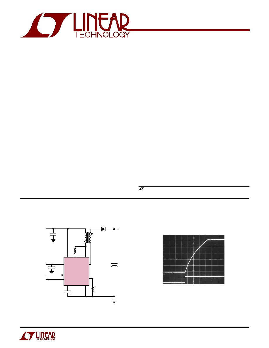
Photoflash Capacitor
Charger with Automatic Refresh
The LT
®
3420 charges high voltage photoflash capacitors
quickly and efficiently. Intended for use in both digital and
film cameras, the device uses a flyback topology to achieve
efficiencies up to 4 times better than competing flash
modules. A unique adaptive off-time control algorithm
maintains current-limited continuous mode transformer
operation through the entire charge cycle, eliminating
high inrush current often found in modules.
The LT3420 output voltage sensing scheme monitors the
flyback voltage to indirectly regulate the output voltage,
eliminating an output resistor divider or discrete zener
diode. This feature allows the capacitor to be held at a fully
charged state without excessive power consumption.
Automatic refresh (which can be defeated) allows the
capacitor to remain charged while consuming average
input current of about 2mA, at a user-defined refresh rate.
A logic high on the CHARGE pin initiates charging, while
the DONE pin signals that the capacitor is fully charged.
, LTC and LT are registered trademarks of Linear Technology Corporation.
Figure 1. 320V Photoflash Capacitor Charging Circuit
3420 F01
+
V
CC
CHARGE
DONE
SEC
R
REF
LT3420
V
BAT
R
FB
SW
C
T
GND
C2
4.7
µ
F
0.1
µ
F
C1
4.7
µ
F
V
BAT
1.8V TO 10V
V
CC
2.5V TO 10V
CHARGE
DONE
51.1k
T1
1:12
320V
3,4
5,6
8
1
2k
D1
C1, C2: 4.7
µ
F, X5R or X7R, 10V
C3: RUBYCON 220
µ
F PHOTOFLASH CAPACITOR
T1: TDK SRW10EPC-U01H003 FLYBACK TRANSFORMER
D1: GENERAL SEMICONDUCTOR GSD2004S SOT-23
DUAL DIODE. DIODES CONNECTED IN SERIES
DANGER HIGH VOLTAGE
OPERATION BY HIGH VOLTAGE
TRAINED PERSONEL ONLY
C3
220
µ
F
330V
PHOTOFLASH
CAPACITOR
4
9
8
10
5
1
7
6
3
2
Charging Waveform
V
OUT
50V/DIV
V
CHARGE
5V/DIV
1s/DIV
3420 F01b
V
BAT
= 5V
LT3420
2
3420f
V
CC
Voltage .............................................................. 16V
V
BAT
Voltage ............................................................ 16V
SW Voltage (Note 2) ................................................ 38V
SEC Current ......................................................
±
200mA
R
FB
Current ...........................................................
±
3mA
R
REF
Voltage ........................................................... 2.5V
CHARGE Voltage ...................................................... 16V
CT Voltage .............................................................. 1.5V
DONE Voltage .......................................................... 16V
Current into DONE Pin ..........................................
±
1mA
Maximum Junction Temperature .......................... 125
°
C
Operating Ambient Temperature Range
(Note 3) .............................................. 40
°
C to 85
°
C
Storage Temperature Range ................. 65
°
C to 150
°
C
Lead Temperature (Soldering, 10 sec).................. 300
°
C
ORDER PART
NUMBER
MS PART MARKING
T
JMAX
= 125
°
C,
JA
= 100
°
C/W,
JC
= 45
°
C/W
(4-LAYER BOARD)
LTYH
LT3420EMS
ABSOLUTE AXI U
RATI GS
W
W
W
U
PACKAGE/ORDER I FOR ATIO
U
U
W
(Note 1)
ELECTRICAL CHARACTERISTICS
The
q
denotes the specifications which apply over the full operating
temperature range, otherwise specifications are at T
A
= 25
°
C. V
CC
= V
BAT
= 3.3V, V
CHARGE
= V
CC
unless otherwise noted. (Note 2)
PARAMETER
CONDITIONS
MIN
TYP
MAX
UNITS
Minimum Operating Voltage, V
CC
q
2.2
2.5
V
Maximum Operating Voltage, V
CC
16
V
V
CC
UVLO Hysteresis
40
mV
Minimum V
BAT
Voltage
1.6
1.8
V
Maximum V
BAT
Voltage
16
V
V
BAT
UVLO Hysteresis
275
mV
R
REF
Threshold Voltage
0.98
1.00
1.02
V
q
0.975
1.025
V
R
REF
Pin Bias Current
V
RREF
= 0V, Switching
2
4
µ
A
V
RFB
= V
BAT
0.2V (Note 4)
Quiescent Current
V
RREF
= 1.1V, Not Switching
90
130
µ
A
Quiescent Current in Shutdown
V
CHARGE
= 0V, V
IN
= 3.3V
0.01
1
µ
A
Primary Side Current Limit
(Note 5)
1.2
1.4
1.6
A
Secondary Side Current Limit
(Note 5)
20
40
50
mA
Leakage Blanking Pulse Width
200
ns
Refresh Timer Charge/Discharge Current
V
CT
= 0.75V
1.5
2.5
3.5
µ
A
Refresh Timer Upper Threshold
0.9
1.0
1.1
V
Refresh Timer Lower Threshold
0.45
0.5
0.55
V
Switch V
CESAT
SW = 1A
220
340
mV
Switch Leakage Current
V
SW
= 38V
0.01
1
µ
A
Consult LTC Marketing for parts specified with wider operating temperature ranges.
1
2
3
4
5
R
REF
V
BAT
R
FB
V
CC
GND
10
9
8
7
6
C
T
CHARGE
DONE
SEC
SW
TOP VIEW
MS10 PACKAGE
10-LEAD PLASTIC MSOP
LT3420
3
3420f
Note 1: Absolute Maximum Ratings are those values beyond which the life
of a device may be impaired.
Note 2: Rated breakdown with LT3420 in power delivery mode and power
switch off.
Note 3: The LT3420 is guaranteed to meet performance specifications
from 0
°
C to 70
°
C. Specifications over the 40
°
C to 85
°
C operating
PARAMETER
CONDITIONS
MIN
TYP
MAX
UNITS
CHARGE Input Voltage High
1.5
V
CHARGE Input Voltage Low
0.2
V
CHARGE Pin Bias Current
V
CHARGE
= 3V
4.5
15
µ
A
V
CHARGE
= 0V
0.01
0.1
µ
A
DONE Output Signal High
100k from V
CC
to DONE
3.3
V
DONE Output Signal Low
33
µ
A into DONE Pin
100
200
mV
ELECTRICAL CHARACTERISTICS
The
q
denotes the specifications which apply over the full operating
temperature range, otherwise specifications are at T
A
= 25
°
C. V
CC
= V
BAT
= 3.3V, V
CHARGE
= V
CC
unless otherwise noted. (Note 2)
temperature range are assured by design, characterization and correlation
with statistical process controls.
Note 4: Bias current flows out of R
FB
pin.
Note 5: Current limit guaranteed by design and/or correlation to static test.
TYPICAL PERFOR A CE CHARACTERISTICS
U
W
Output Voltage in Refresh Mode
Output Voltage in Refresh Mode
Charge Time
TEMPERATURE (
°
C)
50
V
OUT
(V)
100
3420 G01
0
50
335
330
325
320
315
310
305
300
295
25
25
75
125
FIGURE 1 CIRCUIT
V
CC
= 3.3V
V
BAT
= 3.3V
V
IN
(V)
2.5
V
OUT
(V)
8.5
3420 G02
7.0
4.0
5.5
10
FIGURE 1 CIRCUIT
V
CC
= V
IN
V
BAT
= V
IN
T
A
= 25
°
C
335
330
325
320
315
310
305
300
295
V
BAT
(V)
2
TIME (s)
10
3420 G03
4
6
8
10
8
6
4
2
0
V
OUT
CHARGED
FROM
50V TO 320V
T
A
= 25
°
C
FIGURE 1 CIRCUIT
UNLESS OTHERWISE
NOTED.
C
OUT
= 220
µ
F
C
OUT
= 100
µ
F
LT3420
4
3420f
Charge Pin Input Current
Primary Current Limit
Secondary Current Limit
V
CC
Minimum Operating Voltage
Quiescent Current in Refresh Mode
V
BAT
Minimum Operating Voltage
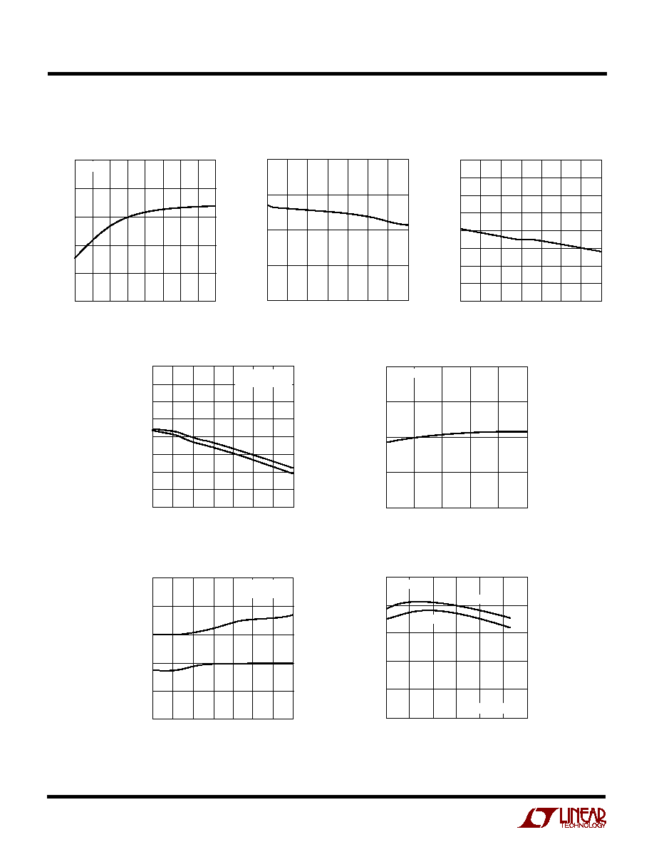
TYPICAL PERFOR A CE CHARACTERISTICS
U
W
Efficiency for Figure 1 Circuit
CHARGE PIN VOLTAGE (V)
2
CURRENT (
µ
A)
10
8
6
4
2
0
5
7
10
3420 G04
3
4
6
8
9
T
A
= 25
°
C
TEMPERATURE (
°
C)
50
CURRENT (A)
3420 G05
0
50
100
1.7
1.5
1.3
1.1
0.9
25
25
75
125
TEMPERATURE (
°
C)
50
CURRENT (mA)
100
3420 G06
0
50
60
55
50
45
40
35
30
25
20
25
25
75
125
TEMPERATURE (
°
C)
50
V
CC
PIN VOLTAGE (V)
100
3420 G07
0
50
2.6
2.5
2.4
2.3
2.2
2.1
2.0
1.9
1.8
25
25
75
125
V
+
V
ENABLE VOLTAGE
IS HYSTERETIC
V
CC
(V)
2.5
QUIESCENT CURRENT (
µ
A)
10
3420 G08
5.5
8.5
140
120
100
80
60
4.0
7.0
T
A
= 25
°
C
TEMPERATURE (
°
C)
50
V
BAT
PIN VOLTAGE (V)
100
3420 G09
0
50
25
25
75
125
2.0
1.8
1.6
1.4
1.2
1.0
V
+
V
ENABLE VOLTAGE
IS HYSTERETIC
EFFICIENCY (%)
3420 G10
90
80
70
60
50
40
V
OUT
(V)
100
200
300
50
150
350
250
V
CC
= V
BAT
= V
IN
V
IN
= 3.3V
V
IN
= 5V
T
A
= 25
°
C

LT3420
5
3420f
U
U
U
PI FU CTIO S
R
REF
(Pin 1): Reference Resistor Pin. Place a resistor (R2)
from the R
REF
pin to GND. 2k is recommended.
V
BAT
(Pin 2): Battery Voltage Input. This pin should be
connected to the power supply or battery, which supplies
power to transformer T1. Must be locally bypassed.
R
FB
(Pin 3): Feedback Resistor Pin. Place a resistor (R1)
from the SW pin to the R
FB
pin. Set R1 according to the
following formula:
R
R
N
R
N V
V
SEC
OUT
D
1
2
1 4
2
2
=
+
+
[
]
( . ·
)
(
)
V
OUT
: Desired Output Voltage
N: Transformer Turns Ratio
R
SEC
: Transformer Secondary Resistance
V
D
: Diode Forward Voltage Drop
V
CC
(Pin 4): Input Supply Pin. Must be locally bypassed
with a 4.7
µ
F or larger ceramic capacitor.
GND (Pin 5): Ground. Tie directly to local ground plane.
SW (Pin 6): Switch Pin. This is the collector of the internal
NPN power switch. Minimize the metal trace area con-
nected to this pin to minimize EMI.
SEC (Pin 7): Transformer Secondary Pin. Tie one end of
the transformer secondary to this pin. Take care to use the
correct phasing of the transformer (Refer to Figure 1).
DONE (Pin 8): Done Output Pin. Open collector NPN
output. DONE is pulled low whenever the chip is delivering
power to the output and goes high when power delivery
stops.
CHARGE (Pin 9): Charge Pin. Drive CHARGE high (1.5V or
more) to commence charging of the output capacitor.
Drive to 0.2V or less to put the part in shutdown mode.
C
T
(Pin 10): Refresh Timer Capacitor Pin. Place a capacitor
from the C
T
pin to GND to set the refresh timer sample rate
according to the following formula:
C
T
= 2.5 · 10
6
· t
REFRESH
t
REFRESH
: Desired Refresh Period in Seconds.