 | ÐлекÑÑоннÑй компоненÑ: LTC1401C | СкаÑаÑÑ:  PDF PDF  ZIP ZIP |
/home/web/doc/html/liner/177737
1
LTC1401
Complete
SO-8, 12-Bit, 200ksps
ADC with Shutdown
The LTC
®
1401 is a complete 200ksps, 12-bit A/D con-
verter that converts 0V to 2.048V unipolar input and draws
only 15mW from a single 3V supply. This easy-to-use
device comes complete with a 315ns sample-and-hold
and a precision reference. Maximum DC specifications
include
±
1LSB INL,
±
1LSB DNL and 45ppm/
°
C full-scale
drift over temperature.
The LTC1401 has three power saving modes: Nap and
Sleep, through the serial interface and Shutdown by
setting the SHDN pin to zero. In Nap mode, it consumes
only 1.5mW of power and can wake up and convert
immediately. In Sleep (Shutdown) mode, it consumes
19.5
µ
W (13.5
µ
W) of power typically. Upon power-up
from Sleep or Shutdown mode, a reference ready (REFRDY)
signal is available in the serial word to indicate that the
reference has settled and the chip is ready to convert.
The 3-wire serial port allows compact and efficient data
transfer to a wide range of microprocessors, microcon-
trollers and DSPs.
DESCRIPTIO
N
U
FEATURES
s
Complete 12-Bit ADC with Reference in SO-8
s
Single Supply 3V Operation
s
Sample Rate: 200ksps
s
Power Dissipation: 15mW (Typ)
s
68dB S/(N + D) and 72dB THD at 50kHz
s
No Missing Codes Over Temperature
s
Nap Mode with Instant Wake-Up: 1.5mW
s
Sleep Mode: 19.5
µ
W
s
Shutdown Mode: 13.5
µ
W
s
High Impedance Analog Input
s
Input Range (0.5mV/LSB): 0V to 2.048V
s
Internal Reference Can Be Overdriven Externally
s
3-Wire Interface to DSPs and Processors (SPI and
MICROWIRE
TM
Compatible)
Single 3V Supply, 200kHz, 12-Bit Sampling A/D Converter
s
Low Power and Battery-Operated Systems
s
Handheld or Portable Instruments
s
High Speed Data Acquisition
s
Digital Signal Processing
s
Multiplexed Data Acquisition Systems
s
Telecommunication
s
Digital Radio
s
Spectrum Analysis
APPLICATIO
N
S
U
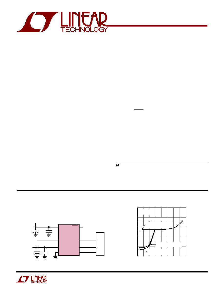
TYPICAL APPLICATIO
N
U
V
CC
A
IN
V
REF
GND
SHDN
CONV
CLK
D
OUT
P1.4
P1.3
P1.2
LTC1401
MPU
SERIAL
DATA LINK
+
0.1
µ
F
10
µ
F
+
0.1
µ
F
10
µ
F
1.20V
ANALOG INPUT
(0V TO 2.048V)
4
3
2
1
5
6
7
8
3V
1401 TA01
SAMPLE RATE (Hz)
0.01
SUPPLY CURRENT (mA)
1
10
100
10
1k
1M
LTC1401 · TA02
0.1
0.01
0.001
0.1
1
100
10k 100k
NORMAL CONVERSION
NAP MODE
BETWEEN CONVERSION
SHUTDOWN MODE
BETWEEN CONVERSION
SLEEP MODE BETWEEN
CONVERSION
3.2MHz CLOCK
T
A
= 25
°
C
Power Consumption vs Sample Rate
, LTC and LT are registered trademarks of Linear Technology Corporation.
MICROWIRE is a trademark of National Semiconductor Corporation.
2
LTC1401
ABSOLUTE
M
AXI
M
U
M
RATINGS
W
W
W
U
(Notes 1, 2)
Supply Voltage (V
CC
) ................................................. 7V
Analog Input Voltage (Note 3) ..... 0.3V to (V
CC
+ 0.3V)
Digital Input Voltage (Note 4) .................... 0.3V to 12V
Digital Output Voltage .................. 0.3V to (V
CC
+ 0.3V)
Power Dissipation .............................................. 300mW
Operating Ambient Temperature Range
LTC1401C................................................ 0
°
C to 70
°
C
LTC1401I ............................................ 40
°
C to 85
°
C
Operating Junction Temperature ......................... 125
°
C
Storage Temperature Range ................. 65
°
C to 150
°
C
Lead Temperature (Soldering, 10 sec).................. 300
°
C
PACKAGE/ORDER I
N
FOR
M
ATIO
N
W
U
U
T
JMAX
= 125
°
C,
JA
= 130
°
C/ W
TOP VIEW
V
CC
A
IN
V
REF
GND
SHDN
CONV
CLK
D
OUT
S8 PACKAGE
8-LEAD PLASTIC SO
1
2
3
4
8
7
6
5
Consult factory for PDIP packages and Military grade parts.
LTC1401CS8
LTC1401IS8
1401
1401I
ORDER PART
NUMBER
S8 PART MARKING
SYMBOL
PARAMETER
CONDITIONS
MIN
TYP
MAX
UNITS
V
CC
Supply Voltage
2.7
3.0
3.6
V
I
CC
Supply Current
f
SAMPLE
= 200ksps
q
5
10
mA
Nap Mode
q
0.5
1.0
mA
Sleep Mode
q
6.5
15
µ
A
Shutdown Mode
q
4.5
10
µ
A
P
D
Power Dissipation
f
SAMPLE
= 200ksps
q
15
30
mW
Nap Mode
q
1.5
3.0
mW
Sleep Mode
q
19.5
45
µ
W
Shutdown Mode
q
13.5
30
µ
W
POWER REQUIRE E TS
W
U
(Note 5)
SYMBOL
PARAMETER
CONDITIONS
MIN
TYP
MAX
UNITS
V
IN
Analog Input Range
q
0 to 2.048
V
I
IN
Analog Input Leakage Current
During Conversions (Hold Mode)
q
±
1
µ
A
C
IN
Analog Input Capacitance
Between Conversions (Sample Mode)
45
pF
During Conversions (Hold Mode)
5
pF
PUT
U
I
A
A
U
LOG
(Note 5)
I TER AL REFERE CE CHARACTERISTICS
U
U
U
(Note 5)
PARAMETER
CONDITIONS
MIN
TYP
MAX
UNITS
V
REF
Output Voltage
I
OUT
= 0
1.180
1.200
1.220
V
V
REF
Output Tempco
I
OUT
= 0
q
±
10
±
45
ppm/
°
C
V
REF
Line Regulation
2.7V
V
CC
3.6V
0.01
LSB/ V
V
REF
Load Regulation
0
I
OUT
1mA
2
LSB/mA
V
REF
Wake-Up Time from Sleep or Shutdown Mode
C
VREF
= 10
µ
F
3
ms
3
LTC1401
PARAMETER
CONDITIONS
MIN
TYP
MAX
UNITS
Resolution (No Missing Codes)
q
12
Bits
Integral Linearity Error
(Note 7)
q
±
1
LSB
Differential Linearity Error
q
±
1
LSB
Offset Error
±
6
LSB
q
±
8
LSB
Full-Scale Error
±
15
LSB
Full-Scale Tempco
I
OUT(REF)
= 0
q
±
10
±
45
ppm/
°
C
C
C
HARA TERISTICS
CO
U
VERTER
With internal reference (Note 5)
SYMBOL
PARAMETER
CONDITIONS
MIN
TYP
MAX
UNITS
S/(N + D) Signal-to-Noise
50kHz Input Signal
q
65
68
dB
Plus Distortion Ratio
100kHz Input Signal
65
dB
THD
Total Harmonic Distortion
50kHz Input Signal
q
72
65
dB
Up to 5th Harmonic
100kHz Input Signal
66
dB
Peak Harmonic or
50kHz Input Signal
q
74
65
dB
Spurious Noise
100kHz Input Signal
67
dB
IMD
Intermodulation Distortion
f
IN1
= 49.853kHz, f
IN2
= 53.076kHz
69
dB
Full Power Bandwidth
2
MHz
Full Linear Bandwidth (S/(N + D)
68dB)
50
kHz
ACCURACY
IC
DY
U
W
A
SYMBOL
PARAMETER
CONDITIONS
MIN
TYP
MAX
UNITS
V
IH
High Level Input Voltage
V
CC
= 3.6V
q
2.0
V
V
IL
Low Level Input Voltage
V
CC
= 2.7V
q
0.8
V
I
IN
Digital Input Current
V
IN
= 0V to V
CC
q
±
10
µ
A
C
IN
Digital Input Capacitance
5
pF
V
OH
High Level Output Voltage
V
CC
= 2.7V, I
O
= 10
µ
A
q
2.40
2.64
V
V
CC
= 2.7V, I
O
= 200
µ
A
q
2.25
2.50
V
V
OL
Low Level Output Voltage
V
CC
= 2.7V, I
O
= 400
µ
A
q
0.13
0.4
V
I
OZ
Hi-Z Output Leakage D
OUT
V
OUT
= 0V to V
CC
q
±
10
µ
A
C
OZ
Hi-Z Output Capacitance D
OUT
15
pF
I
SOURCE
Output Source Current
V
OUT
= 0
5
mA
I
SINK
Output Sink Current
V
OUT
= V
CC
10
mA
(Note 5)
DIGITAL I PUTS A
N
D OUTPUTS
U
U
(Note 5)
4
LTC1401
SYMBOL
PARAMETER
CONDITIONS
MIN
TYP
MAX
UNITS
f
SAMPLE(MAX)
Maximum Sampling Frequency
q
200
kHz
t
CONV
Conversion Time
f
CLK
= 3.2MHz
q
4.1
µ
s
t
ACQ
Acquisition Time
315
ns
f
CLK
CLK Frequency
q
0.1
3.2
MHz
t
CLK
CLK Pulse Width
(Note 6)
q
60
ns
t
WK(NAP)
Time to Wake Up from Nap Mode
350
ns
t
1
CLK Pulse Width to Return to Active Mode
q
60
ns
t
2
CONV
to CLK
Setup Time
q
100
ns
t
3
CONV
After Leading CLK
q
0
ns
t
4
CONV Pulse Width
(Note 8)
q
50
ns
t
5
Time from CLK
to Sample Mode
80
ns
t
6
Aperture Delay of Sample-and-Hold
Jitter < 50ps
45
ns
t
7
Minimum Delay Between Conversion
(Note 6)
q
350
550
ns
t
8
Delay Time, CLK
to D
OUT
Valid
C
LOAD
= 20pF
q
60
120
ns
t
9
Delay Time, CLK
to D
OUT
Hi-Z
C
LOAD
= 20pF
q
60
120
ns
t
10
Time from Previous Data Remains Valid After CLK
C
LOAD
= 20pF
q
15
50
ns
(Note 5)
TI I G CHARACTERISTICS
W U
The
q
denotes specifications which apply over the full operating
temperature range; all other limits and typicals apply to T
A
= 25
°
C.
Note 1: Absolute Maximum Ratings are those values beyond which the life
of a device may be impaired.
Note 2: All voltage values are with respect to GND.
Note 3: When these pin voltages are taken below GND or above V
CC
, they
will be clamped by internal diodes. This product can handle input currents
greater than 40mA without latch-up if the pin is driven below GND or
above V
CC
.
Note 4: When these pin voltages are taken below GND, they will be clamped
by internal diodes. This product can handle input currents greater than 40mA
without latch-up if the pin is driven below GND. These pins are not clamped
to V
CC
.
Note 5: V
CC
= 3V, f
SAMPLE
= 200kHz, t
r
= t
f
= 5ns unless otherwise
specified.
Note 6: Guaranteed by design, not subject to test.
Note 7: Integral nonlinearity is defined as the deviation of a code from a
straight line passing through the actual endpoints of the transfer curve.
The deviation is measured from the center of the quantization band.
Note 8: The rising edge of CONV starts a conversion. If CONV returns low
at a bit decision point during the conversion, it can create small errors. For
best performance, ensure that CONV returns low either within 120ns after
the conversion starts (i.e., before the first bit decision) or after the 14
clock cycles. (Figure 13 Timing Diagram).
5
LTC1401
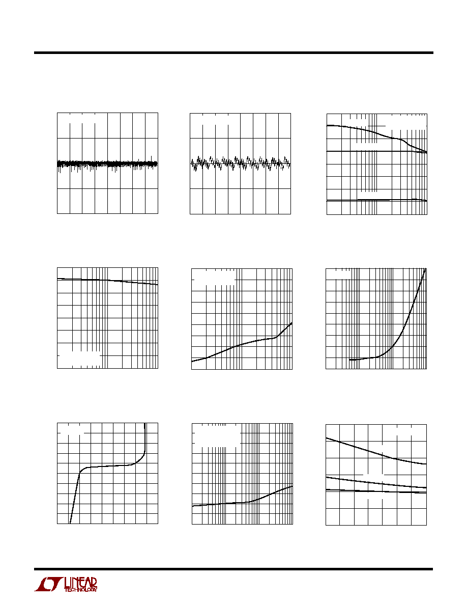
TYPICAL PERFOR
M
A
N
CE CHARACTERISTICS
U
W
CODE
0
1.0
DNL ERROR (LSBs)
0.5
0
0.5
1.0
512
1024
1536
2048
LTC1401 · TPC01
2560
3072
3584
4096
f
SAMPLE
= 200kHz
Differential Nonlinearity vs
Output Code
INPUT FREQUENCY (kHz)
10
0
SIGNAL/(NOISE + DISTORTION)(dB)
10
20
30
40
80
100
1000
LTC1401 · TPC03
50
60
70
V
IN
= 0dB
V
IN
= 20dB
V
IN
= 60dB
T
A
= 25
°
C
f
SAMPLE
= 200kHz
S/(N + D) vs Input Frequency
and Amplitude
Acquisition Time vs
Source Impedance
SOURCE RESISTANCE (
)
10
2500
t
ACQ
(ns)
3000
3500
4000
4500
100
1k
10k
LTC1401 · TPC06
2000
1500
500
0
1000
T
A
= 25
°
C
Signal-to-Noise Ratio (Without
Harmonics) vs Input Frequency
INPUT FREQUENCY (kHz)
10
0
SIGNAL-TO-NOISE RATIO (dB)
10
20
30
40
80
100
1000
LTC1401 · TPC04
50
60
70
T
A
= 25
°
C
f
SAMPLE
= 200kHz
Reference Voltage vs
Load Current
LOAD CURRENT (mA)
7
0.90
REFERENCE VOLTAGE (V)
0.95
1.05
1.10
1.15
1.40
1.25
5
3
2
2
LTC1401 · TPC07
1.00
1.30
1.35
1.20
6
4
1
0
1
T
A
= 25
°
C
TEMPERATURE (°C)
50
SUPPLY CURRENT (mA)
8
10
12
25
75
LTC1401 · TPC09
6
4
25
0
50
100
125
2
0
V
IN
= 3.6V
V
IN
= 3V
V
IN
= 2.7V
f
SAMPLE
= 200kHz
Supply Current vs Temperature
Integral Nonlinearity vs
Output Code
Peak Harmonic or Spurious Noise
vs Input Frequency
INPUT FREQUENCY (kHz)
10
50
SPURIOUS-FREE DYNAMIC RANGE (dB)
40
30
80
90
70
60
20
10
100
1000
LTC1401 · TPC05
0
T
A
= 25
°
C
f
SAMPLE
= 200kHz
Power Supply Feedthrough vs
Ripple Frequency
CODE
0
1.0
INL ERROR (LSBs)
0.5
0
0.5
1.0
512
1024
1536
2048
LTC1401 · TPC02
2560
3072
3584
4096
f
SAMPLE
= 200kHz
RIPPLE FREQUENCY (kHz)
1
60
POWER SUPPLY FEEDTHROUGH (dB)
50
40
30
20
10
100
1000
LTC1401 · TPC08
70
80
90
100
10
0
f
SAMPLE
= 200kHz
f
IN
= 49.853kHz
V
CC
(V
RIPPLE
= 1mV)