Äîêóìåíòàöèÿ è îïèñàíèÿ www.docs.chipfind.ru
1
LTC1420
12-Bit, 10Msps,
Sampling ADC
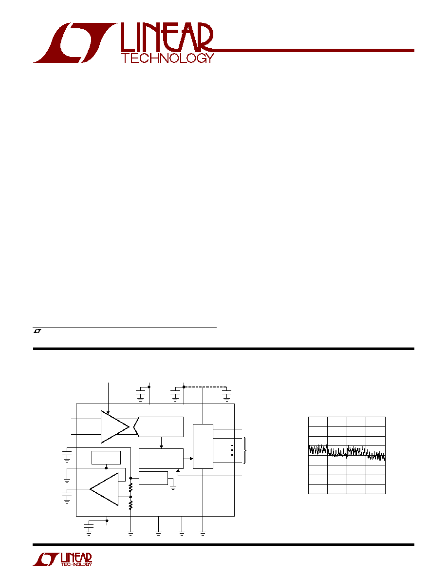
The LTC
®
1420 is a 10Msps, 12-bit sampling A/D converter
that draws only 250mW from either single 5V or dual
±
5V
supplies. This easy-to-use device includes a high dynamic
range sample-and-hold, a precision reference and a PGA
input circuit.
The LTC1420 has a flexible input circuit that allows full-
scale input ranges of
±
2.048V
±
1.024V and
±
0.512V. The
input common mode voltage is arbitrary, though a 2.5V
reference is provided for single supply applications. The
input PGA has a digitally selectable 1x or 2x gain.
Maximum DC specs include
±
1LSB INL and
±
1LSB DNL
over temperature. Outstanding AC performance includes
71dB S/(N + D) and 83dB SFDR at the Nyquist input
frequency of 5MHz.
The unique differential input sample-and-hold can acquire
single-ended or differential input signals up to its 100MHz
bandwidth. The 75dB common mode rejection allows
users to eliminate ground loops and common mode noise
by measuring signals differentially from the source. A
separate output logic supply allows direct connection to
3V components.
s
10Msps Sample Rate
s
Single 5V Supply or
±
5V Supplies
s
Integral Nonlinearity Error <0.35LSB
s
Differential Nonlinearity <0.25LSB
s
71dB S/(N + D) and 83dB SFDR at Nyquist
s
100MHz Full-Power Bandwidth Sampling
s
±
2.048V,
±
1.024V and
±
0.512V Bipolar Input Range
s
Input PGA
s
Out-of-Range Indicator
s
True Differential Inputs with 75dB CMRR
s
Power Dissipation: 250mW
s
28-Pin Narrow SSOP Package
s
Telecommunications
s
Digital Signal Processing
s
Multiplexed Data Acquisition Systems
s
High Speed Data Acquisition
s
Spectral Analysis
s
Imaging Systems
, LTC and LT are registered trademarks of Linear Technology Corporation.
Typical INL Curve
CODE
0
1024
2048
3072
4096
INL (LSBs)
1420 TA02
1.00
0.75
0.50
0.25
0
0.25
0.50
0.75
1.00
DIGITAL CORRECTION
LOGIC
OUTPUT
BUFFERS
1420 TA01
MODE SELECT
PIPELINED 12-BIT ADC
S/H
0V OR 5V
V
CM
GAIN
5V
V
DD
V
DD
OV
DD
28
7
23
22
21
OPTIONAL 3V
LOGIC SUPPLY
OF
D11 (MSB)
D0 (LSB)
CLK
27
10
20
26
10MHz CLK
DIGITAL
OUTPUT
SENSE
V
REF
A
IN
+
A
IN
VIN
+
3
4
5
2
1
24
8
25
6
OGND
GND
GND
V
SS
GND
2.048V
2.5V
REFERENCE
1
µ
F
5V
5V
1
µ
F
1
µ
F
1
µ
F
1
µ
F
1
µ
F
FEATURES
DESCRIPTIO
U
APPLICATIO S
U
TYPICAL APPLICATIO
U
2
LTC1420
SYMBOL
PARAMETER
CONDITIONS
MIN
TYP
MAX
UNITS
V
IN
Analog Input Range (Note 9)
V
REF
= 4.096V (SENSE = 0V), GAIN = 5V (1
×
)
q
±
2.048
V
+A
IN
(A
IN
)
V
REF
= 4.096V (SENSE = 0V), GAIN = 0V (2
×
)
q
±
1.024
V
V
REF
= 2.048V (SENSE = V
REF
), GAIN = 5V (1
×
)
q
±
1.024
V
V
REF
= 2.048V (SENSE = V
REF
), GAIN = 0V (2
×
)
q
±
0.512
V
External V
REF
(SENSE = 5V), GAIN = 5V (1
×
)
q
±
V
REF
/2
V
External V
REF
(SENSE = 5V), GAIN = 0V (2
×
)
q
±
V
REF
/4
V
I
IN
Analog Input Leakage Current
q
±
20
µ
A
C
IN
Analog Input Capacitance
Between Conversions
12
pF
During Conversions
6
pF
t
ACQ
Sample-and-Hold Acquisition Time
30
ns
t
AP
Sample-and-Hold Aperture Delay Time
250
ps
t
jitter
Sample-and-Hold Aperture Delay Time Jitter
0.6
ps
CMRR
Analog Input Common Mode Rejection Ratio
2.048V < (A
IN
= +A
IN
) < 2.048V
75
dB
ABSOLUTE AXI U
RATI GS
W
W
W
U
PACKAGE/ORDER I FOR ATIO
U
U
W
0V
DD
= V
DD
(Notes 1, 2)
Supply Voltage (V
DD
) ................................................. 6V
Negative Supply Voltage (V
SS
) ................................ 6V
Total Supply Voltage (V
DD
to V
SS
) ........................... 12V
Analog Input Voltage
(Note 3) ............................. (V
SS
0.3V) to (V
DD
+ 0.3V)
Digital Input Voltage
(Note 4) ............................. (V
SS
0.3V) to (V
DD
+ 0.3V)
Digital Output Voltage ........ (V
SS
0.3V) to (V
DD
+ 0.3V)
Power Dissipation .............................................. 500mW
Operating Temperature Range
LTC1420C ............................................... 0
°
C to 70
°
C
LTC1420I ............................................ 40
°
C to 85
°
C
Storage Temperature Range ................. 65
°
C to 150
°
C
Lead Temperature (Soldering, 10 sec).................. 300
°
C
PARAMETER
CONDITIONS
MIN
TYP
MAX
UNITS
Resolution (No Missing Codes)
q
12
Bits
Integral Linearity Error
(Note 7)
q
±
0.35
±
1
LSB
Differential Linearity Error
q
±
0.25
±
1
LSB
Offset Error
(Note 8)
±
5
12
LSB
q
16
LSB
Full-Scale Error
±
10
30
LSB
Full-Scale Tempco
I
OUT(REF)
= 0
±
15
ppm/
°
C
ORDER PART
NUMBER
LTC1420CGN
LTC1420IGN
Consult factory for Military grade parts.
T
JMAX
= 110
°
C,
JA
= 110
°
C/W
1
2
3
4
5
6
7
8
9
10
11
12
13
14
TOP VIEW
GN PACKAGE
28-LEAD PLASTIC SSOP
28
27
26
25
24
23
22
21
20
19
18
17
16
15
+A
IN
A
IN
V
CM
SENSE
V
REF
GND
V
DD
GND
D11 (MSB)
D10
D9
D8
D7
D6
GAIN
OF
CLK
V
SS
GND
V
DD
OV
DD
OGND
D0
D1
D2
D3
D4
D5
The
q
denotes the specifications which apply over the full operating
temperature range, otherwise specifications are at T
A
= 25
°
C. With Internal 4.096V Reference. Specifications are guaranteed for both
dual supply and single supply operation. (Note 5)
The
q
denotes the specifications which apply over the full operating temperature range, otherwise
specifications are at T
A
= 25
°
C. Specifications are guaranteed for both dual supply and single supply operation. (Note 5)
CO
N
VERTER CHARACTERISTICS
U
A ALOG I PUT
U
U
3
LTC1420
PARAMETER
CONDITIONS
MIN
TYP
MAX
UNITS
V
CM
Output Voltage
I
OUT
= 0
2.475
2.50
2.525
V
V
CM
Output Tempco
I
OUT
= 0
±
15
ppm/
°
C
V
CM
Line Regulation
4.75V
V
DD
5.25V
0.6
mV/V
5.25V
V
SS
4.75V
0.03
mV/V
V
CM
Output Resistance
0.1mA
I
OUT
0.1mA
8
V
REF
Output Voltage
SENSE = GND, I
OUT
= 0
4.096
V
SENSE = V
REF
, I
OUT
= 0
2.048
V
SENSE = V
DD
Drive V
REF
with
V
External Reference
V
REF
Output Tempco
±
15
ppm/
°
C
SYMBOL
PARAMETER
CONDITIONS
MIN
TYP
MAX
UNITS
S/(N + D)
Signal-to-Noise Plus Distortion Ratio
1MHz Input Signal
q
68.5
71.4
dB
5MHz Input Signal
q
68
71.0
dB
THD
Total Harmonic Distortion
1MHz Input Signal, First 5 Harmonics
q
84
77
dB
5MHz Input Signal, First 5 Harmonics
q
81
73
dB
SFDR
Peak Harmonic or Spurious Noise
1MHz Input Signal
q
85
78.5
dB
5MHz Input Signal
q
83
75
dB
IMD
Intermodulation Distortion
f
IN1
= 29.37kHz, f
IN2
= 32.446kHz
80
dB
Full-Power Bandwidth
100
MHz
Input Referred Noise
±
2.048V Input Range
0.22
LSB
RMS
±
1.024V Input Range, 2x Mode (SENSE = GAIN = 0V)
0.33
LSB
RMS
Overvoltage Recovery Time
1.5x FS Input to 0 (Settling to 1LSB)
15
ns
Full-Scale Step Acquisition Time
Settling to 1LSB
15
ns
SYMBOL
PARAMETER
CONDITIONS
MIN
TYP
MAX
UNITS
V
IH
High Level Input Voltage
V
DD
= 5.25V, V
SS
= 0V
q
2.4
V
V
DD
= 5.25V, V
SS
= 5V
q
3.5
V
V
IL
Low Level Input Voltage
V
DD
= 4.75V, V
SS
= 0V
q
0.8
V
V
DD
= 4.75V, V
SS
= 5V
q
1
V
I
IN
Digital Input Current
V
IN
= 0V to V
DD
q
±
10
µ
A
C
IN
Digital Input Capacitance
1.8
pF
V
OH
High Level Output Voltage
0V
DD
= 4.75V, I
O
= 10
µ
A
4.74
V
0V
DD
= 4.75V, I
O
= 200
µ
A
q
4.0
4.71
V
0V
DD
= 2.7V, I
O
= 10
µ
A
2.6
V
0V
DD
= 2.7V, I
O
= 200
µ
A
q
2.3
V
V
OL
Low Level Output Voltage
0V
DD
= 4.75V, I
O
= 160
µ
A
0.05
V
0V
DD
= 4.75V, I
O
= 1.6mA
q
0.10
0.4
V
0V
DD
= 2.7V, I
O
= 160
µ
A
0.05
V
0V
DD
= 2.7V, I
O
= 1.6mA
q
0.10
0.4
V
I
SOURCE
Output Source Current
V
OUT
= 0V
50
mA
I
SINK
Output Sink Current
V
OUT
= V
DD
35
mA
The
q
denotes the specifications which apply over the full
operating temperature range, otherwise specifications are at T
A
= 25
°
C. Specifications are guaranteed for both dual supply and single
supply operation. (Note 5)
T
A
= 25
°
C. Specifications are guaranteed for both dual supply and single supply operation. (Note 5)
The
q
denotes the specifications which apply over the full operating temperature range,
otherwise specifications are at T
A
= 25
°
C. V
DD
= 5V, V
SS
= 5V, f
SAMPLE
= 10MHz, V
REF
= 4.096V. + A
IN
= 0.1dBFS single ended input,
A
IN
= 0V. (Note 6)
DY
A
IC ACCURACY
U
W
I
N
TER
N
AL REFERE
N
CE CHARACTERISTICS
U
U
U
DIGITAL I PUTS A D DIGITAL OUTPUTS
U
U
4
LTC1420
SYMBOL
PARAMETER
CONDITIONS
MIN
TYP
MAX
UNITS
V
DD
Positive Supply Voltage
(Note 10)
4.75
5.25
V
OV
DD
Output Supply Voltage
(Note 10)
2.7
5.25
V
V
SS
Negative Supply Voltage
Dual Supply Mode
5.25
4.75
V
Single Supply Mode
0
V
I
DD
Positive Supply Current
q
48
58
mA
I
SS
Negative Supply Current
q
1.4
2.5
mA
P
D
Power Dissipation
q
250
300
mW
SYMBOL
PARAMETER
CONDITIONS
MIN
TYP
MAX
UNITS
f
SAMPLE
Maximum Sampling Frequency
q
0.02
10
MHz
t
CONV
Conversion Time
q
70
90
ns
t
ACQ
Acquisition Time
q
10
30
ns
t
H
CLK High Time
q
20
50
ns
t
L
CLK Low Time
q
20
50
ns
t
AP
Aperature Delay of Sample-and-Hold
250
ps
Note 1: Absolute Maximum Ratings are those values beyond which the life
of a device may be impaired.
Note 2: All voltage values are with respect to ground with GND and OGND
wired together (unless otherwise noted).
Note 3: When these pin voltages are taken below V
SS
or above V
DD
, they
will be clamped by internal diodes. This product can handle input currents
greater than 100mA below V
SS
or above V
DD
without latchup.
Note 4: When these pin voltages are taken below V
SS
they will be clamped
by internal diodes. This product can handle input currents greater than
100mA below V
SS
without latchup. GAIN is not clamped to V
DD
. When CLK
is taken above V
DD
, it will be clamped by an internal diode. The CLK pin
can handle input currents of greater than 100mA above V
DD
without
latchup.
Note 5: V
DD
= 5V, V
SS
= 5V or 0V, f
SAMPLE
= 10MHz, t
r
= t
f
= 5ns unless
otherwise specified.
Note 6: Dynamic specifications are guaranteed for dual supply operation
with a single-ended + A
IN
input and A
IN
grounded. For single supply
dynamic specifications, refer to the Typical Performance Characteristics.
Note 7: Integral nonlinearity is defined as the deviation of a code from a
straight line passing through the actual endpoints of the transfer curve.
The deviation is measured from the center of the quantization band.
Note 8: Bipolar offset is the offset voltage measured from 0.5LSB
when the output code flickers between 0000 0000 0000 and
1111 1111 1111.
Note 9: Guaranteed by design, not subject to test.
Note 10: Recommended operating conditions.
The
q
denotes the specifications which apply over the full operating temperature
range, otherwise specifications are at T
A
= 25
°
C. Specifications are guaranteed for both dual supply and single supply operation.
(Note 5)
The
q
denotes the specifications which apply over the full operating temperature
range, otherwise specifications are at T
A
= 25
°
C. Specifications are guaranteed for both dual supply and single supply operation.
(Note 5)
POWER REQUIRE E TS
W
U
TI I G CHARACTERISTICS
U
W
5
LTC1420
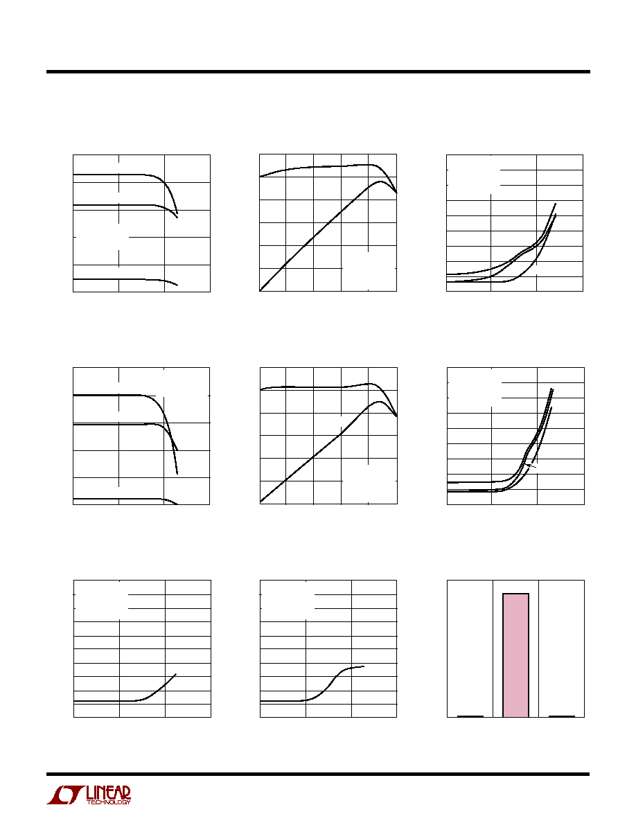
TYPICAL PERFOR A CE CHARACTERISTICS
U
W
S/(N+D) vs Input Frequency
and Amplitude
INPUT FREQUENCY (MHz)
0.1
S/(N + D) (dB)
60
65
1420 G01
55
50
1
10
100
75
70
V
IN
= 0dB
V
IN
= 6dB
V
IN
= 20dB
DUAL SUPPLIES
±
2.048V RANGE
GAIN = 1
×
INPUT FREQUENCY (MHz)
0.1
S/(N + D) (dB)
60
65
1420 G02
55
50
1
10
100
75
70
V
IN
= 0dB
V
IN
= 6dB
V
IN
= 20dB
SINGLE SUPPLY
±
1.024V RANGE
GAIN = 2
×
INPUT AMPLITUDE (dBFS)
50
40
SFDR (dBc AND dBFS)
50
60
70
80
90
100
dBFS
dBc
40
30
20
10
1420 G03
0
DUAL SUPPLIES
±
2.048V RANGE
GAIN = 1
×
f
IN
= 5MHz
S/(N+D) vs Input Frequency
and Amplitude
Spurious-Free Dynamic Range
vs Input Amplitude
Distortion vs Input Frequency
INPUT FREQUENCY (MHz)
0
95
DISTORTION (dB)
90
80
75
70
10
50
1420 G04
85
1
100
65
60
55
THD
3RD
2ND
DUAL SUPPLIES
±
2.048V RANGE
GAIN = 1
×
A
IN
= 0dBFS
Spurious-Free Dynamic Range
vs Input Amplitude
INPUT AMPLITUDE (dBFS)
50
40
SFDR (dBc AND dBFS)
50
60
70
80
90
100
dBFS
40
30
20
10
1420 G05
0
SINGLE SUPPLY
±
1.024V RANGE
GAIN = 2
×
f
IN
= 5MHz
dBc
Distortion vs Input Frequency
INPUT FREQUENCY (MHz)
0
95
DISTORTION (dB)
90
80
75
70
10
50
1420 G06
85
1
100
65
60
55
THD
2ND
3RD
SINGLE SUPPLY
±
1.024V RANGE
GAIN = 2
×
A
IN
= 0dBFS
SFDR vs Input Frequency,
Differential Input
Grounded Input Histogram
INPUT FREQUENCY (MHz)
0.1
100
SFDR (dB)
90
85
80
75
70
65
1
10
1420 F07
60
55
50
95
100
DUAL SUPPLIES
±
2.048V RANGE
GAIN = 1
×
A
IN
= 0dBFS
SFDR vs Input Frequency,
Differential Input
INPUT FREQUENCY (MHz)
0.1
100
SFDR (dB)
90
85
80
75
70
65
1
10
1420 F08
60
55
50
95
100
SINGLE SUPPLY
±
1.024V RANGE
GAIN = 2
×
A
IN
= 0dBFS
CODE
N 1
1570
410554
V
REF
= 4.096V
GAIN = 1
×
HITS
N
N + 1
1420 F09
1572