 | ÐлекÑÑоннÑй компоненÑ: LTC1430CS | СкаÑаÑÑ:  PDF PDF  ZIP ZIP |
Äîêóìåíòàöèÿ è îïèñàíèÿ www.docs.chipfind.ru
1
LTC1430
High Power Step-Down
Switching Regulator Controller
The LTC
®
1430 is a high power, high efficiency switching
regulator controller optimized for 5V to 3.xV applications.
It includes a precision internal reference and an internal
feedback system that can provide output regulation of
±
1%
over temperature, load current and line voltage shifts. The
LTC1430 uses a synchronous switching architecture with
two N-channel output devices, eliminating the need for a
high power, high cost P-channel device. Additionally, it
senses output current across the drain-source resistance
of the upper N-channel FET, providing an adjustable
current limit without an external low value sense resistor.
The LTC1430 includes a fixed frequency PWM oscillator for
low output ripple under virtually all operating conditions.
The 200kHz free-running clock frequency can be externally
adjusted from 100kHz to above 500kHz. The LTC1430
features low 350
µ
A quiescent current, allowing greater
than 90% efficiency operation in converter designs from
1A to greater than 50A output current. Shutdown mode
drops the LTC1430 supply current to 1
µ
A.
s
High Power 5V to 3.xV Switching Controller:
Can Exceed 10A Output
s
All N-Channel External MOSFETs
s
Constant Frequency Operation--Small Inductor
s
Excellent Output Regulation:
±
1% Over Line, Load
and Temperature Variations
s
High Efficiency: Over 95% Possible
s
Fixed Frequency Operation
s
No Low Value Sense Resistor Needed
s
Outputs Can Drive External FETs with Up to
10,000pF Gate Capacitance
s
Quiescent Current: 350
µ
A Typ, 1
µ
A in Shutdown
s
Fast Transient Response
s
Adjustable or Fixed 3.3V Output
s
Available in 8- and 16-Lead PDIP and SO Packages
, LTC and LT are registered trademarks of Linear Technology Corporation.
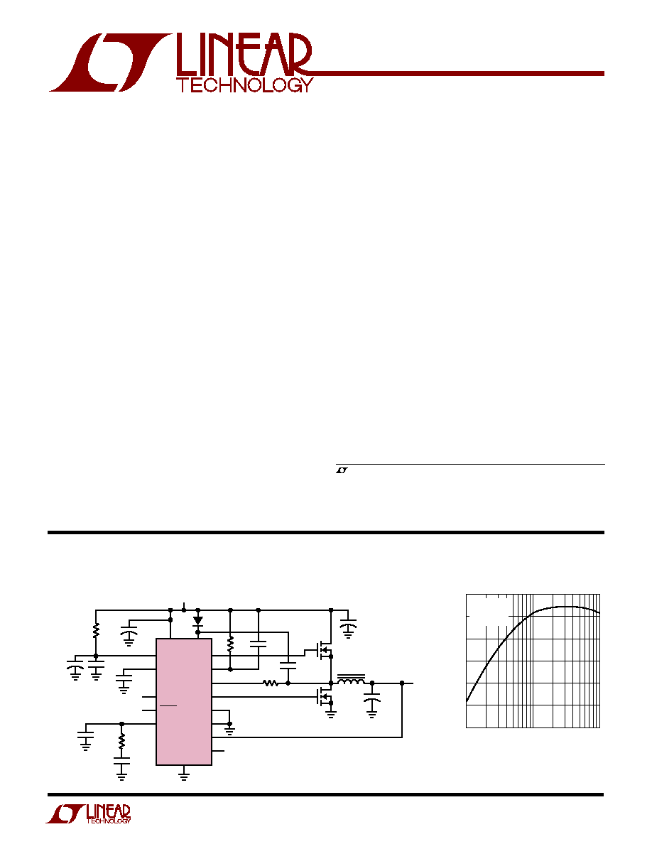
LOAD CURRENT (A)
40
70
100
90
80
50
60
EFFICIENCY (%)
10
LTC1430 · TA02
0.1
1
T
A
= 25
°
C
V
IN
= 5V
V
OUT
= 3.3V
Efficiency
+
C
IN
220
µ
F
×
4
C
OUT
330
µ
F
×
6
+
+
+
L1, 2.8
µ
H
PV
CC1
V
CC
FREQSET
SHDN
COMP
SS
PV
CC2
PGND
GND
G1
I
FB
I
MAX
G2
NC
LTC1430 · TA01
SHUTDOWN
FB
NC
C
IN
: AVX-TPSE227M010R0100
C
OUT
: AVX-TPSE337M006R0100
L1: ETQP6F1R6SFA
M1A, M1B, M2: MOTOROLA MTD20N03HL
SENSE
+
LTC1430
SENSE
16k
100
R
C
7.5k
C
C
4700pF
C1
220pF
1N4148
1k
0.1
µ
F
1
µ
F
0.01
µ
F
0.1
µ
F
4.7
µ
F
0.1
µ
F
3.3V
10A
M1A, M1B
2 IN PARALLEL
M2
V
IN
5V
Typical 5V to 3.3V, 10A Application
s
Power Supply for P6 and Pentium
®
Microprocessors
s
High Power 5V to 3.xV Regulators
s
Local Regulation for Dual Voltage Logic Boards
s
Low Voltage, High Current Battery Regulation
Pentium is a registered trademark of Intel Corporation.
APPLICATIO S
U
FEATURES
TYPICAL APPLICATIO
U
DESCRIPTIO
U
2
LTC1430
Supply Voltage
V
CC
....................................................................... 9V
PV
CC1, 2
.............................................................. 13V
Input Voltage
I
FB
......................................................... 0.3V to 18V
All Other Inputs ...................... 0.3V to (V
CC
+ 0.3V)
Operating Temperature Range
LTC1430C .............................................. 0
°
C to 70
°
C
LTC1430I ........................................... 40
°
C to 85
°
C
Storage Temperature Range ................ 65
°
C to 150
°
C
Lead Temperature (Soldering, 10 sec)................. 300
°
C
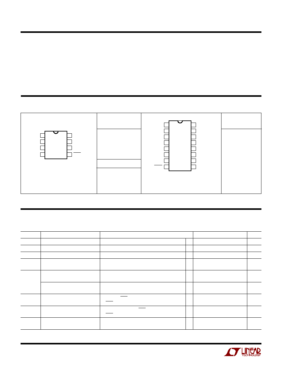
ORDER
PART NUMBER
ORDER
PART NUMBER
LTC1430CN
LTC1430CS
LTC1430IS
LTC1430CN8
LTC1430CS8
S8 PART MARKING
1430
SYMBOL
PARAMETER
CONDITIONS
MIN
TYP
MAX
UNITS
V
CC
Supply Voltage
q
4
8
V
PV
CC
PV
CC1
, PV
CC2
q
13
V
V
OUT
Output Voltage
Figure 1
q
3.30
V
V
FB
Feedback Voltage
Figure 1, SENSE
+
and SENSE
Floating (LTC1430C)
q
1.25
1.265
1.28
V
Figure 1, SENSE
+
and SENSE
Floating (LTC1430I)
q
1.23
1.265
1.29
V
V
OUT
Output Load Regulation
Figure 1, I
OUT
= 0A to 10A (Note 3) (LTC1430C)
q
5
20
mV
Figure 1, I
OUT
= 0A to 10A (Note 3) (LTC1430I)
5
mV
Output Line Regulation
Figure 1, V
CC
= 4.75V to 5.25V (Note 3) (LTC1430C)
q
1
5
mV
Figure 1, V
CC
= 4.75V to 5.25V (Note 3) (LTC1430I)
1
mV
IV
CC
Supply Current (V
CC
Only)
Figure 2, V
SHDN
= V
CC
q
350
700
µ
A
V
SHDN
= 0V
1
10
µ
A
IPV
CC
Supply Current (PV
CC
)
Figure 2, PV
CC
= 5V, V
SHDN
= V
CC
(Note 4)
1.5
mA
V
SHDN
= 0V
0.1
µ
A
f
OSC
Internal Oscillator Frequency
FREQSET Floating (LTC1430C)
q
140
200
260
kHz
FREQSET Floating (LTC1430I)
q
130
200
300
kHz
The
q
denotes the specifications which apply over the full operating
temperature range, otherwise specifications are at T
A
= 25
°
C. V
CC
= 5V unless otherwise noted. (Note 2)
Consult factory for Industrial and Military grade parts.
T
JMAX
= 150
°
C,
JA
= 100
°
C/W (N8)
T
JMAX
= 150
°
C,
JA
= 150
°
C/W (S8)
1
2
3
4
8
7
6
5
TOP VIEW
G1
PV
CC1
GND
FB
G2
V
CC
/PV
CC2
COMP
SHDN
N8 PACKAGE
8-LEAD PDIP
S8 PACKAGE
8-LEAD PLASTIC SO
T
JMAX
= 150
°
C,
JA
= 70
°
C/W (N)
T
JMAX
= 150
°
C,
JA
= 110
°
C/W (S)
1
2
3
4
5
6
7
8
TOP VIEW
S PACKAGE
16-LEAD PLASTIC SO
N PACKAGE
16-LEAD PDIP
16
15
14
13
12
11
10
9
G1
PV
CC1
PGND
GND
SENSE
FB
SENSE
+
SHDN
G2
PV
CC2
V
CC
I
FB
I
MAX
FREQSET
COMP
SS
(Note 1)
ABSOLUTE AXI U
RATI GS
W
W
W
U
PACKAGE/ORDER I FOR ATIO
U
U
W
ELECTRICAL CHARACTERISTICS
3
LTC1430
SYMBOL
PARAMETER
CONDITIONS
MIN
TYP
MAX
UNITS
Note 1: Absolute Maximum Ratings are those values beyond which the life
of a device may be impaired.
Note 2: All currents into device pins are positive; all currents out of device
pins are negative. All voltages are referenced to ground unless otherwise
specified.
Note 3: This parameter is guaranteed by correlation and is not tested
directly.
Note 4: Supply current in normal operation is dominated by the current
needed to charge and discharge the external FET gates. This will vary with
the LTC1430 operating frequency, operating voltage and the external FETs
used.
Note 5: The I
LIM
amplifier can sink but cannot source current. Under
normal (not current limited) operation, the I
LIM
output current will be zero.
The
q
denotes the specifications which apply over the full operating
temperature range, otherwise specifications are at T
A
= 25
°
C. V
CC
= 5V unless otherwise noted. (Note 2)
ELECTRICAL CHARACTERISTICS
V
IH
SHDN Input High Voltage
q
2.4
V
V
IL
SHDN Input Low Voltage
q
0.8
V
I
IN
SHDN Input Current
q
±
0.1
±
1
µ
A
A
V
Error Amplifier Open-Loop DC Gain
(LTC1430I)
q
40
48
dB
gm
V
Error Amplifier Transconductance
(LTC1430C)
650
µ
Mho
(LTC1430I)
q
300
650
1200
µ
Mho
gm
I
I
LIM
Amplifier Transconductance
(Note 5)
1300
µ
Mho
I
MAX
I
MAX
Sink Current
V
I(MAX)
= V
CC
(LTC1430C)
q
8
12
16
µ
A
V
I(MAX)
= V
CC
(LTC1430I)
q
8
12
17
µ
A
I
SS
Soft-Start Source Current
V
SS
= 0 (LTC1430C)
q
8
12
16
µ
A
V
SS
= 0 (LTC1430I)
q
8
12
17
µ
A
t
r
, t
s
Driver Rise/Fall Time
Figure 3, PV
CC1
= PV
CC2
= 5V
80
250
ns
t
NOV
Driver Non-Overlap Time
Figure 3, PV
CC1
= PV
CC2
= 5V
25
130
250
ns
DC
MAX
Maximum Duty Cycle
V
COMP
= V
CC
(LTC1430C)
q
90
96
%
V
COMP
= V
CC
, V
FB
= 0 (LTC1430I)
q
90
96
%
V
COMP
= V
CC
, V
FB
= 1.265V (LTC1430I)
q
83
88
%

4
LTC1430
G1 (Pin 1/Pin 1): Driver Output 1. Connect this pin to the
gate of the upper N-channel MOSFET, M1. This output will
swing from PV
CC1
to PGND. It will always be low when G2
is high.
PV
CC1
(Pin 2/Pin 2): Power V
CC
for Driver 1. This is the
power supply input for G1. G1 will swing from PGND to
PV
CC1
. PV
CC1
must be connected to a potential of at least
PV
CC
+ V
GS(ON)
(M1). This potential can be generated
using an external supply or a simple charge pump con-
nected to the switching node between the upper MOSFET
and the lower MOSFET; see Applications Information for
details.
PGND (Pin 3/Pin 3): Power Ground. Both drivers return to
this pin. It should be connected to a low impedance ground
in close proximity to the source of M2. 8-lead parts have
PGND and GND tied together at pin 3.
GND (Pin 4/Pin 3): Signal Ground. All low power internal
circuitry returns to this pin. To minimize regulation errors
due to ground currents, GND should be connected to
PGND right at the LTC1430. 8-lead parts have PGND and
GND tied together internally at pin 3.
SENSE
, FB, SENSE
+
(Pins 5, 6, 7/Pin 4): These three
pins connect to the internal resistor divider and to the
internal feedback node. To use the internal divider to set
the output voltage to 3.3V, connect SENSE
+
to the positive
terminal of the output capacitor and SENSE
to the nega-
tive terminal. FB should be left floating in applications that
use the internal divider. To use an external resistor divider
to set the output voltage, float SENSE
+
and SENSE
and
connect the external resistor divider to FB.
SHDN (Pin 8/Pin 5): Shutdown. A TTL compatible low
level at SHDN for longer than 50
µ
s puts the LTC1430 into
shutdown mode. In shutdown, G1 and G2 go low, all
internal circuits are disabled and the quiescent current
drops to 10
µ
A max. A TTL compatible high level at SHDN
allows the part to operate normally.
SS (Pin 9/NA): Soft-Start. The SS pin allows an external
capacitor to be connected to implement a soft-start func-
tion. An external capacitor from SS to ground controls the
start-up time and also compensates the current limit loop,
allowing the LTC1430 to enter and exit current limit
cleanly. See Applications Information for more details.
COMP (Pin 10/Pin 6): External Compensation. The COMP
pin is connected directly to the output of the error amplifier
and the input of the PWM. An RC network is used at this
node to compensate the feedback loop to provide opti-
mum transient response. See Applications Information for
compensation details.
FREQSET (Pin 11/NA): Frequency Set. This pin is used to
set the free running frequency of the internal oscillator.
With the pin floating, the oscillator runs at about 200kHz.
A resistor from FREQSET to ground will speed up the
oscillator; a resistor to V
CC
will slow it down. See Applica-
tions Information for resistor selection details.
I
MAX
(Pin 12/NA): Current Limit Set. I
MAX
sets the thresh-
old for the internal current limit comparator. If I
FB
drops
below I
MAX
with G1 on, the LTC1430 will go into current
limit. I
MAX
has a 12
µ
A pull-down to GND. It can be adjusted
with an external resistor to PV
CC
or an external voltage
source.
I
FB
(Pin 13/NA): Current Limit Sense. Connect to the
switched node at the source of M1 and the drain of M2
through a 1k resistor. The 1k resistor is required to prevent
voltage transients from damaging I
FB
. This pin can be
taken up to 18V above GND without damage.
V
CC
(Pin 14/Pin 7): Power Supply. All low power internal
circuits draw their supply from this pin. Connect to a clean
power supply, separate from the main PV
CC
supply at the
drain of M1. This pin requires a 4.7
µ
F bypass capacitor.
8-lead parts have V
CC
and PV
CC2
tied together at pin 7 and
require a 10
µ
F bypass to GND.
PV
CC2
(Pin 15/Pin 7): Power V
CC
for Driver 2. This is the
power supply input for G2. G2 will swing from GND to
PV
CC2
. PV
CC2
is usually connected to the main high power
supply. The 8-lead parts have V
CC
and PV
CC2
tied together
at pin 7 and require a 10
µ
F bypass to GND.
G2 (Pin 16/Pin 8): Driver Output 2. Connect this pin to the
gate of the lower N-channel MOSFET, M2. This output will
swing from PV
CC2
to PGND. It will always be low when G1
is high.
(16-Lead Package/8-Lead Package)
PI FU CTIO S
U
U
U
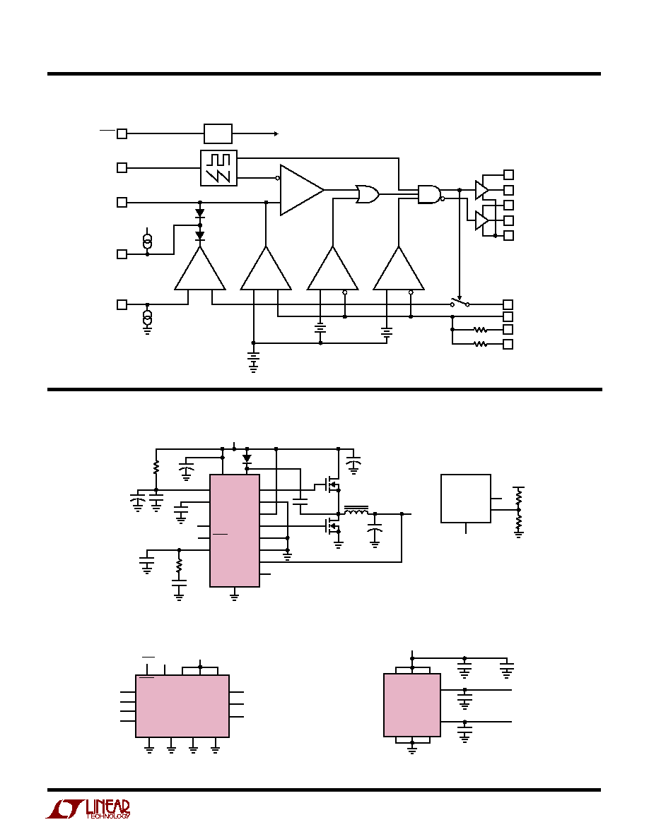
5
LTC1430
+
+
I
LIM
FB
MIN
PWM
MAX
+
40mV
20.1k
+
1.26V
12
µ
A
+
40mV
12
µ
A
12.4k
PV
CC1
SHDN
FREQSET
COMP
SS
I
MAX
V
CC
PV
CC2
G1
G2
PGND
I
FB
FB
SENSE
+
SENSE
LTC1430 · BD
INTERNAL
SHUTDOWN
50
µ
s
DELAY
BLOCK DIAGRA
W
Figure 1
Figure 2
Figure 3
LTC1430
PV
CC1
5V
V
CC
PV
CC2
GND
PGND
G1 RISE/FALL
G2 RISE/FALL
G1
G2
10,000pF
LTC1430 · TC03
10,000pF
10
µ
F
0.1
µ
F
SHDN
V
SHDN
I
MAX
FREQSET
COMP
SS
NC
NC
NC
NC
V
CC
PV
CC2
LTC1430
PV
CC
PV
CC1
I
FB
GND
PGND
SENSE
+
SENSE
LTC1430 · TC02
G1
G2
FB
NC
NC
NC
V
CC
+
C
IN
220
µ
F
×
4
C
OUT
330
µ
F
×
6
+
+
+
2.7
µ
H/15A
PV
CC1
V
CC
FREQSET
SHDN
COMP
SS
PV
CC2
PV
CC
= 5V
PGND
GND
G1
I
FB
I
MAX
G2
NC
LTC1430 · F01
SHUTDOWN
FB
NC
SENSE
+
LTC1430
SENSE
1.61k
1k
FB
NC
NC
SENSE
+
SENSE
LTC1430
FB MEASUREMENT
V
OUT
100
R
C
7.5k
C
C
4700pF
C1
220pF
1N4148
1
µ
F
0.01
µ
F
0.1
µ
F
4.7
µ
F
0.1
µ
F
3.3V
M1A, M1B
2 IN PARALLEL
M2
M1A, M1B, M2: MOTOROLA MTD20N03HL
C
IN
: AVX-TPSE227M010R0100
C
OUT
: AVX-TPSE337M006R0100
TEST CIRCUITS