 | –≠–ª–µ–∫—Ç—Ä–æ–Ω–Ω—ã–π –∫–æ–º–ø–æ–Ω–µ–Ω—Ç: LTC1436A | –°–∫–∞—á–∞—Ç—å:  PDF PDF  ZIP ZIP |
1
LTC1436A
LTC1436A-PLL/LTC1437A
High Efficiency Low Noise
Synchronous Step-Down
Switching Regulators
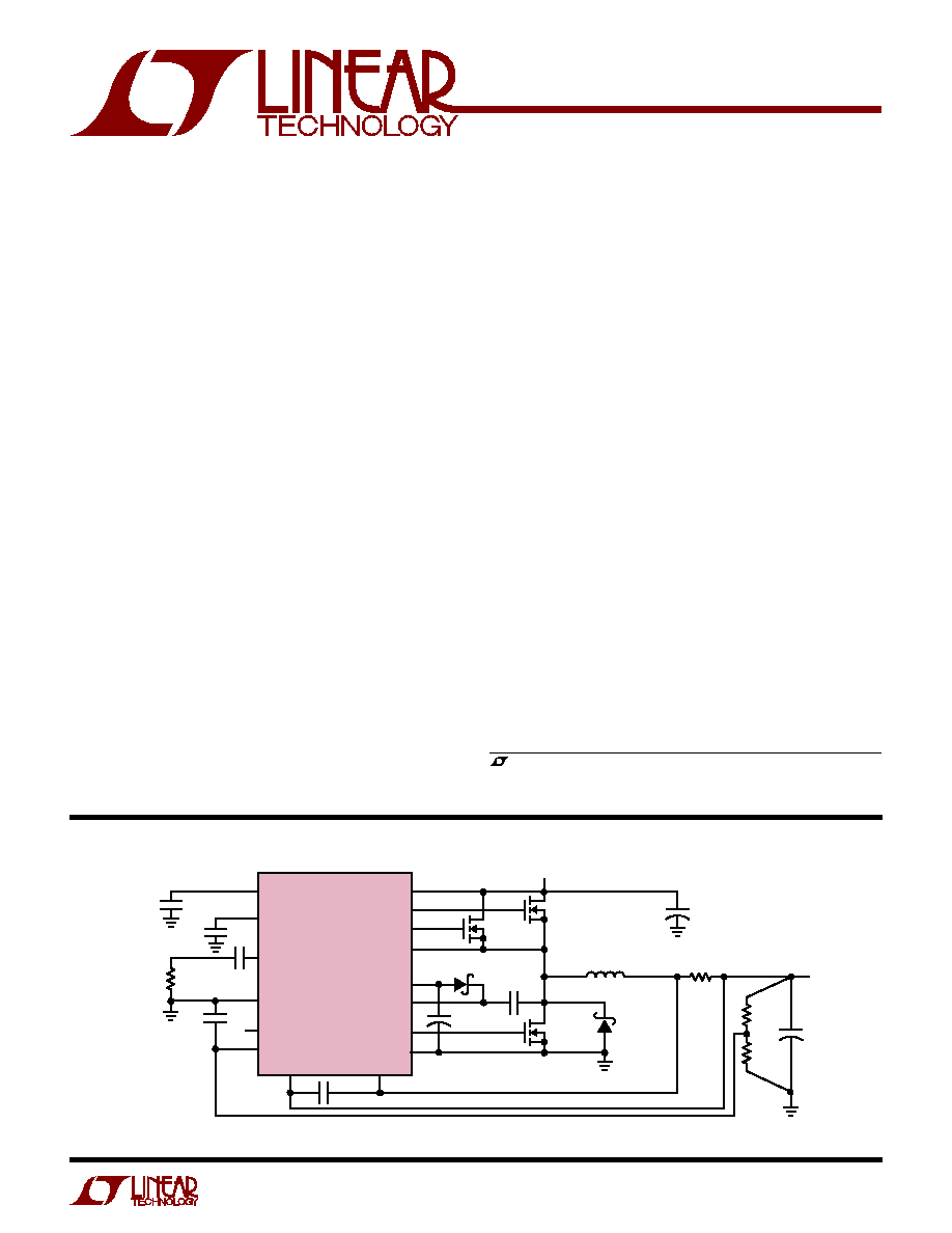
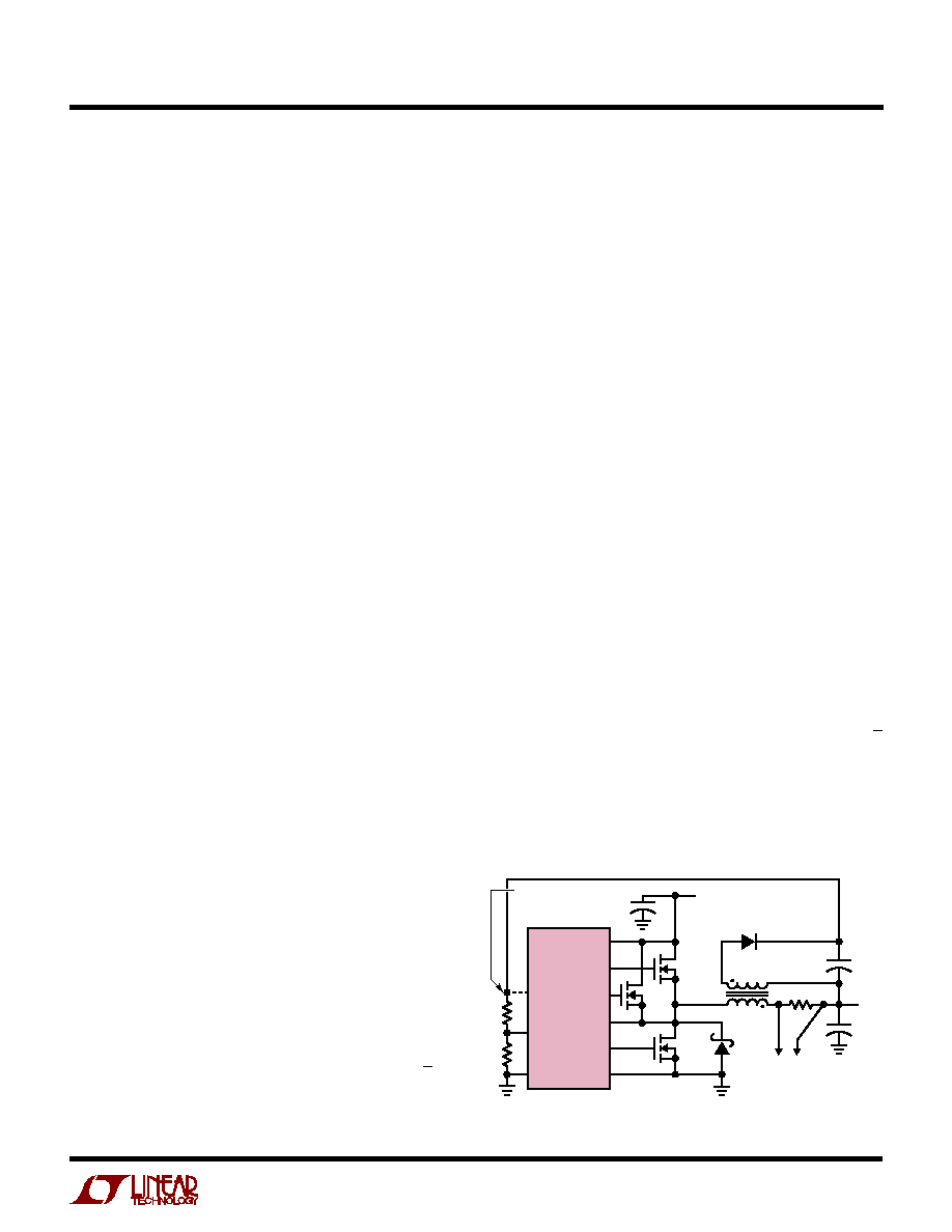
Figure 1. High Efficiency Step-Down Converter
FEATURES
DESCRIPTIO
N
U
, LTC and LT are registered trademarks of Linear Technology Corporation.
Adaptive Power is a trademark of Linear Technology Corporation.
s
Maintains Constant Frequency at Low Output Currents
s
Dual N-Channel MOSFET Synchronous Drive
s
Programmable Fixed Frequency (PLL Lockable)
s
Wide V
IN
Range: 3.5V to 36V Operation
s
Low Minimum On-Time (
300ns) for High
Frequency, Low Duty Cycle Applications
s
Very Low Dropout Operation: 99% Duty Cycle
s
Low Dropout, 0.5A Linear Regulator for CPU I/O
or Low Noise Audio Supplies
s
Built-In Power-On Reset Timer
s
Programmable Soft Start
s
Low-Battery Detector
s
Remote Output Voltage Sense
s
Foldback Current Limiting (Optional)
s
Pin Selectable Output Voltage
s
Logic Controlled Micropower Shutdown: I
Q
< 25
µ
A
s
Output Voltages from 1.19V to 9V
s
Available in 24-Lead Narrow SSOP and 28-Lead
SSOP Packages
The LTC
Æ
1436A/LTC1437A are synchronous step-down
switching regulator controllers that drive external
N-channel power MOSFETs in a phase lockable, fixed
frequency architecture. The Adaptive Power
TM
output stage
selectively drives two N-channel MOSFETs at frequencies
up to 400kHz while reducing switching losses to maintain
high efficiencies at low output currents.
An auxiliary 0.5A linear regulator using an external PNP
pass device provides a low noise, low dropout voltage
source. A secondary winding feedback control pin (SFB)
guarantees regulation regardless of the load on the main
output by forcing continuous operation.
An additional comparator is available for use as a low-
battery detector. A power-on reset timer (POR) is included
which generates a signal delayed by 65536/f
CLK
(300ms
typically) after the output is within 5% of the regulated
output voltage. Internal resistive dividers provide pin
selectable output voltages with remote sense capability.
The operating current level is user-programmable via an
external current sense resistor. Wide input supply range
allows operation from 3.5V to 30V (36V maximum).
APPLICATIO
N
S
U
s
Notebook and Palmtop Computers, PDAs
s
Cellular Telephones and Wireless Modems
s
Portable Instruments
s
Battery-Operated Devices
s
DC Power Distribution Systems
TYPICAL APPLICATIO
N
U
C
OSC
RUN/SS
V
IN
V
PROG
+
+
+
V
IN
4.5V TO 22V
C
B
0.1
µ
F
4.7
µ
F
1000pF
LTC1436A
M1
Si4412DY
L1
4.7
µ
H
R
SENSE
0.02
C
OUT
100
µ
F
6.3V
◊
2
R1
35.7k
R2
102k
C
IN
22
µ
F
35V
◊
2
C
OSC
43pF
C
SS
0.1
µ
F
C
C
510pF
100pF
R
C
10k
V
OUT
1.6V
5A
M2
Si4412DY
D1
MBRS140T3
SENSE
+
SENSE
≠
SGND
M3
IRLML2803
D
B
CMDSH-3
TGL
TGS
SW
BOOST
BG
PGND
1436 F01
INTV
CC
I
TH
V
OSENSE
2
LTC1436A
LTC1436-PLL-A/LTC1437A
ABSOLUTE
M
AXI
M
U
M
RATINGS
W
W
W
U
Input Supply Voltage (V
IN
).........................36V to ≠ 0.3V
Topside Driver Supply Voltage (Boost) ......42V to ≠ 0.3V
Switch Voltage (SW)............................. V
IN
+ 5V to ≠ 5V
EXTV
CC
Voltage .........................................10V to ≠ 0.3V
POR, LBO Voltages ....................................12V to ≠ 0.3V
AUXFB Voltage ..........................................20V to ≠ 0.3V
AUXDR Voltage ..........................................28V to ≠ 0.3V
SENSE
+
, SENSE
≠
,
V
OSENSE
Voltages.................. INTV
CC
+ 0.3V to ≠ 0.3V
V
PROG
Voltage..................................... INTV
CC
to ≠ 0.3V
PLL LPF, I
TH
Voltages ............................... 2.7V to ≠ 0.3V
AUXON, PLLIN, SFB,
RUN/SS, LBI Voltages ..........................10V to ≠ 0.3V
Peak Driver Output Current < 10
µ
s (TGL, BG) .......... 2A
Peak Driver Output Current < 10
µ
s (TGS) ......... 250mA
INTV
CC
Output Current ......................................... 50mA
Operating Temperature Range
LTC143XAC ............................................. 0
∞
C to 70
∞
C
LTC143XAI ........................................ ≠ 40
∞
C to 85
∞
C
Junction Temperature (Note 1) ............................. 125
∞
C
Storage Temperature Range ................. ≠ 65
∞
C to 150
∞
C
Lead Temperature (Soldering, 10 sec).................. 300
∞
C
SYMBOL
PARAMETER
CONDITIONS
MIN
TYP
MAX
UNITS
Main Control Loop
I
IN
V
OSENSE
Feedback Current
V
PROG
Pin Open (Note 2)
10
50
nA
V
OUT
Regulated Output Voltage
(Note 2)
1.19V (Adjustable) Selected
V
PROG
Pin Open
q
1.178
1.19
1.202
V
3.3V Selected
V
PROG
= 0V
q
3.220
3.30
3.380
V
5V Selected
V
PROG
= INTV
CC
q
4.900
5.00
5.100
V
T
A
= 25
∞
C, V
IN
= 15V, V
RUN/SS
= 5V unless otherwise noted.
ELECTRICAL CHARACTERISTICS
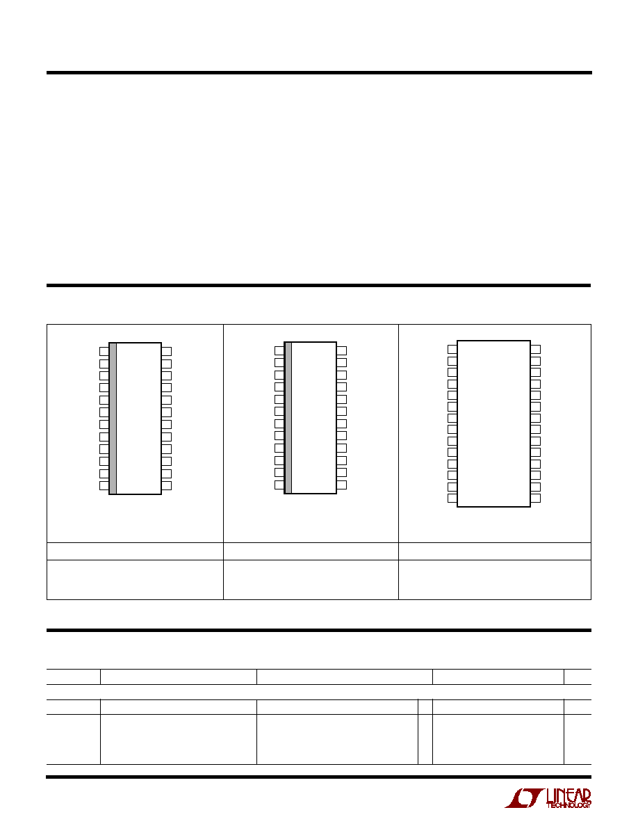
PACKAGE/ORDER I
N
FOR
M
ATIO
N
W
U
U
ORDER PART NUMBER
1
2
3
4
5
6
7
8
9
10
11
12
TOP VIEW
GN PACKAGE
24-LEAD PLASTIC SSOP
(150 MIL SSOP)
24
23
22
21
20
19
18
17
16
15
14
13
PLL LPF
C
OSC
RUN/SS
I
TH
SFB
SGND
V
PROG
V
OSENSE
SENSE
≠
SENSE
+
AUXON
AUXFB
PLLIN
POR
BOOST
TGL
SW
TGS
V
IN
INTV
CC
BG
PGND
EXTV
CC
AUXDR
ORDER PART NUMBER
T
JMAX
= 125
∞
C,
JA
= 95
∞
C/W
TOP VIEW
G PACKAGE
28-LEAD PLASTIC SSOP
28
27
26
25
24
23
22
21
20
19
18
17
16
15
1
2
3
4
5
6
7
8
9
10
11
12
13
14
PLL LPF
C
OSC
RUN/SS
LBO
LBI
I
TH
SFB
SGND
V
PROG
V
OSENSE
NC
SENSE
≠
SENSE
+
AUXON
PLLIN
POR
BOOST
TGL
SW
TGS
V
IN
INTV
CC
DRV
CC
BG
PGND
EXTV
CC
AUXDR
AUXFB
ORDER PART NUMBER
1
2
3
4
5
6
7
8
9
10
11
12
TOP VIEW
GN PACKAGE
24-LEAD PLASTIC SSOP
(150 MIL SSOP)
24
23
22
21
20
19
18
17
16
15
14
13
C
OSC
RUN/SS
LBO
LBI
I
TH
SFB
SGND
V
PROG
V
OSENSE
SENSE
≠
SENSE
+
AUXON
POR
BOOST
TGL
SW
TGS
V
IN
INTV
CC
BG
PGND
EXTV
CC
AUXDR
AUXFB
T
JMAX
= 125
∞
C,
JA
= 110
∞
C/W
T
JMAX
= 125
∞
C,
JA
= 110
∞
C/W
Consult factory for Military grade parts.
LTC1436ACGN
LTC1436AIGN
LTC1436ACGN-PLL
LTC1436AIGN-PLL
LTC1437ACG
LTC1437AIG
3
LTC1436A
LTC1436A-PLL/LTC1437A
ELECTRICAL CHARACTERISTICS
T
A
= 25
∞
C, V
IN
= 15V, V
RUN/SS
= 5V unless otherwise noted.
SYMBOL
PARAMETER
CONDITIONS
MIN
TYP
MAX
UNITS
V
LINEREG
Reference Voltage Line Regulation
V
IN
= 3.6V to 20V (Note 2), V
PROG
Pin Open
0.002
0.01
%/V
V
LOADREG
Output Voltage Load Regulation
I
TH
Sinking 5
µ
A (Note 2)
q
0.5
0.8
%
I
TH
Sourcing 5
µ
A (Note 2)
q
≠ 0.5
≠ 0.8
%
V
SFB
Secondary Feedback Threshold
V
SFB
Ramping Negative
q
1.16
1.19
1.22
V
I
SFB
Secondary Feedback Current
V
SFB
= 1.5V
≠ 1
≠ 2
µ
A
V
OVL
Output Overvoltage Lockout
V
PROG
Pin Open
1.24
1.28
1.32
V
I
PROG
V
PROG
Input Current
0.5V > V
PROG
≠ 3
≠ 6
µ
A
INTV
CC
≠ 0.5V < V
PROG
< INTV
CC
3
6
µ
A
I
Q
Input DC Supply Current
EXTV
CC
= 5V (Note 3)
Normal Mode
3.6V < V
IN
< 30V, V
AUXON
= 0V
280
µ
A
Shutdown
V
RUN/SS
= 0V, 3.6V < V
IN
< 15V
16
25
µ
A
V
RUN/SS
RUN Pin Threshold
q
0.8
1.3
2
V
I
RUN/SS
Soft Start Current Source
V
RUN/SS
= 0V
1.5
3
4.5
µ
A
V
SENSE(MAX)
Maximum Current Sense Threshold
V
OSENSE
= 0V, 5V, V
PROG
Pin Open
130
150
180
mV
t
ON(MIN)
Minimum On-Time
Tested with Square Wave, SENSE
≠
= 1.6V,
250
300
ns
V
SENSE
= 20mV (Note 6)
TGL Transition Time
TGL t
r
Rise Time
C
LOAD
= 3000pF
50
150
ns
TGL t
f
Fall Time
C
LOAD
= 3000pF
50
150
ns
TGS Transition Time
TGS t
r
Rise Time
C
LOAD
= 500pF
90
200
ns
TGS t
f
Fall Time
C
LOAD
= 500pF
50
150
ns
BG Transition Time
BG t
r
Rise Time
C
LOAD
= 3000pF
50
150
ns
BG t
f
Fall Time
C
LOAD
= 3000pF
40
150
ns
Internal V
CC
Regulator
V
INTVCC
Internal V
CC
Voltage
6V < V
IN
< 30V, V
EXTVCC
= 4V
q
4.8
5.0
5.2
V
V
LDO
INT
INTV
CC
Load Regulation
I
INTVCC
= 15mA, V
EXTVCC
= 4V
≠ 0.2
≠ 1
%
V
LDO
EXT
EXTV
CC
Voltage Drop
I
INTVCC
= 15mA, V
EXTVCC
= 5V
130
230
mV
V
EXTVCC
EXTV
CC
Switchover Voltage
I
INTVCC
= 15mA, V
EXTVCC
Ramping Positive
q
4.5
4.7
V
Oscillator and Phase-Locked Loop
f
OSC
Oscillator Frequency
C
OSC
= 100pF, LTC1436 (Note 4),
112
125
138
kHz
LTC1436A-PLL/LTC1437A, V
PLLLPF
= 0V
VCO High
LTC1436A-PLL/LTC1437A, V
PLLLPF
= 2.4V
200
240
kHz
R
PLLIN
PLL IN
Input Resistance
50
k
I
PLLLPF
Phase Detector Output Current
Sinking Capability
f
PLLIN
< f
OSC
10
15
20
µ
A
Sourcing Capability
f
PLLIN
> f
OSC
10
15
20
µ
A
Power-On Reset
V
SATPOR
POR Saturation Voltage
I
POR
= 1.6mA, V
OSENSE
= 1V, V
PROG
Pin Open
0.6
1
V
I
LPOR
POR Leakage
V
POR
= 12V, V
OSENSE
= 1.2V, V
PROG
Pin Open
0.2
1
µ
A
V
THPOR
POR Trip Voltage
V
PROG
Pin Open, V
OSENSE
Ramping Negative
≠ 11
≠ 7.5
≠ 4
%
t
DPOR
POR Delay
V
PROG
Pin Open
65536
Cycles
4
LTC1436A
LTC1436-PLL-A/LTC1437A
ELECTRICAL CHARACTERISTICS
T
A
= 25
∞
C, V
IN
= 15V, V
RUN/SS
= 5V unless otherwise noted.
SYMBOL
PARAMETER
CONDITIONS
MIN
TYP
MAX
UNITS
Low-Battery Comparator
V
SATLBO
LBO Saturation Voltage
I
LBO
= 1.6mA, V
LBI
= 1.1V
0.6
1
V
I
LLBO
LBO Leakage
V
LBO
= 12V, V
LBI
= 1.4V
q
0.01
1
µ
A
V
THLBI
LBI Trip Voltage
High to Low Transition on LBO
q
1.16
1.19
1.22
V
I
INLBI
LBI Input Current
V
LBI
= 1.19V
q
1
50
nA
V
HYSLBO
LBO Hysteresis
20
mV
Auxiliary Regulator/Comparator
I
AUXDR
AUXDR Current
V
EXTVCC
= 0V
Max Current Sinking Capability
V
AUXDR
= 4V, V
AUXFB
= 1.0V, V
AUXON
= 5V
10
15
mA
Control Current
V
AUXDR
= 5V, V
AUXFB
= 1.5V, V
AUXON
= 5V
1
5
µ
A
Leakage When Off
V
AUXDR
= 24V, V
AUXFB
= 1.5V, V
AUXON
= 0V
0.01
1
µ
A
I
IN
AUXFB
AUXFB Input Current
V
AUXFB
= 1.19V, V
AUXON
= 5V
0.01
1
µ
A
I
IN AUXON
AUXON Input Current
V
AUXON
= 5V
0.01
1
µ
A
V
TH AUXON
AUXON Trip Voltage
V
AUXDR
= 4V, V
AUXFB
= 1.0V
1.0
1.19
1.4
V
V
SAT AUXDR
AUXDR Saturation Voltage
I
AUXDR
= 1.6mA, V
AUXFB
= 1.0V, V
AUXON
= 5V
0.4
0.8
V
V
AUXFB
AUXFB Voltage
V
AUXON
= 5V, 11V < V
AUXDR
< 24V (Note 5)
q
11.5
12
12.5
V
V
AUXON
= 5V, 3V < V
AUXDR
< 7V (Note 5)
q
1.14
1.19
1.24
V
V
TH AUXDR
AUXFB Divider Disconnect Voltage
V
AUXON
= 5V (Note 5), Ramping Negative
7.5
8.5
9.5
V
Note 4: Oscillator frequency is tested by measuring the C
OSC
charge and
discharge currents and applying the formula:
f
OSC
(kHz) =
+
≠1
8.4(10
8
)
C
OSC
(pF) + 11
(
)
1
I
CHG
(
)
1
I
DIS
Note 5: The Auxiliary Regulator is tested in a feedback loop which servos
V
AUXFB
to the balance point for the error amplifier. For applications with
V
AUXDR
> 9.5V, V
AUXFB
uses an internal resistive divider. See
Applications Information.
Note 6: The minimum on-time test condition corresponds to an inductor
peak-to-peak ripple current
40% of I
MAX
(see Minimum On-Time
Considerations in the Applications Information section).
The
q
denotes specifications which apply over the full operating
temperature range.
LTC1436ACGN/LTC1436ACGN-PLL/LTC1437ACG: 0
∞
C
T
A
70
∞
C
LTC1436AIGN/LTC1436AIGN-PLL/LTC1437AIG: ≠ 40
∞
C
T
A
85
∞
C
Note 1: T
J
is calculated from the ambient temperature T
A
and power
dissipation P
D
according to the following formulas:
LTC1436ACGN/LTC1436ACGN-PLL/LTC1436AIGN/
LTC1436AIGN-PLL: T
J
= T
A
+ (P
D
)(110
∞
C/W)
LTC1437ACG/LTC1437AIG: T
J
= T
A
+ (P
D
)(95
∞
C/W)
Note 2: The LTC1436A/LTC1437A are tested in a feedback loop which
servos V
OSENSE
to the balance point for the error amplifier
(V
ITH
= 1.19V).
Note 3: Dynamic supply current is higher due to the gate charge being
delivered at the switching frequency. See Applications Information
section.
5
LTC1436A
LTC1436A-PLL/LTC1437A
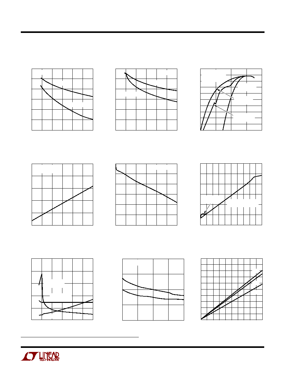
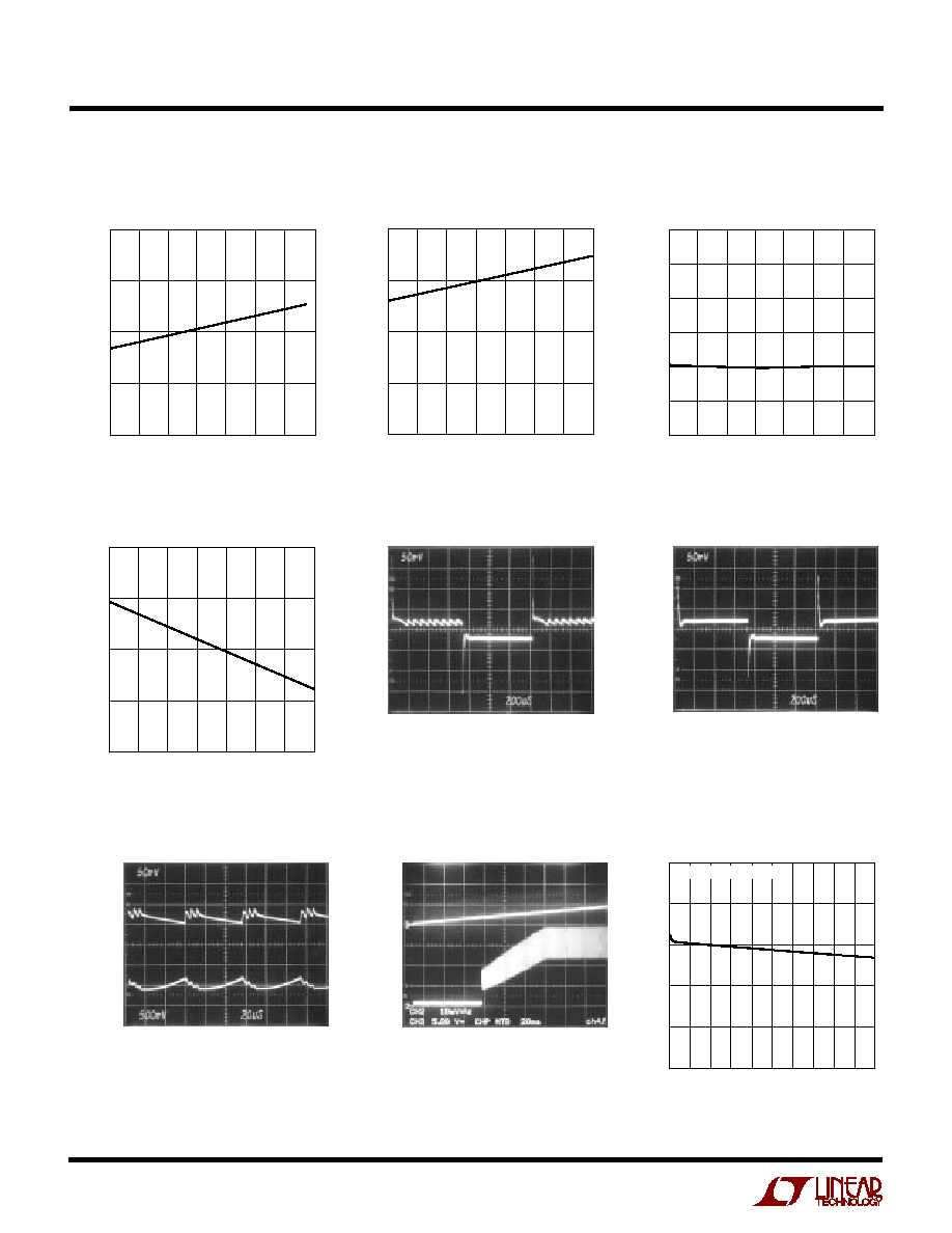
TYPICAL PERFOR
M
A
N
CE CHARACTERISTICS
U
W
Efficiency vs Input Voltage
V
OUT
= 3.3V
V
IN
≠ V
OUT
Dropout Voltage
vs Load Current
Efficiency vs Load Current
V
ITH
Pin Voltage vs Output Current
Efficiency vs Input Voltage
V
OUT
= 5V
Load Regulation
LOAD CURRENT (A)
0.001
50
EFFICIENCY (%)
55
65
70
75
100
85
0.01
0.1
1
1435 G03
60
90
95
80
10
Adaptive Power
MODE
CONTINUOUS
MODE
V
IN
= 10V
V
OUT
= 5V
R
SENSE
= 0.033
Burst Mode
TM
OPERATION
LOAD CURRENT (A)
0
0
V
IN
≠ V
OUT
(V)
0.2
0.1
0.3
0.4
0.5
0.5
1.0
1.5
2.0
1436 G04
2.5
3.0
R
SENSE
= 0.033
V
OUT
DROP OF 5%
LOAD CURRENT (A)
0
V
OUT
(%)
0
0.5
1.0
1.5
2.0
1436 G05
2.5
3.0
≠ 0.25
≠ 0.50
≠ 0.75
≠1.00
≠1.25
≠1.50
R
SENSE
= 0.033
OUTPUT CURRENT (%)
0
V
ITH
(V)
1.0
2.0
3.0
0.5
1.5
2.5
20
40
60
80
1436 G06
100
10
0
30
50
70
90
Burst Mode
OPERATION
CONTINUOUS/Adaptive
Power MODE
Input Supply Current
vs Input Voltage
EXTV
CC
Switch Drop
vs INTV
CC
Load Current
INPUT VOLTAGE (V)
0
0
SUPPLY CURRENT (mA)
SHUTDOWN CURRENT (
µ
A)
0.5
1.0
1.5
2.0
2.5
0
20
40
60
80
100
5
10
15
20
1436 G07
25
30
V
OUT
= 3.3V
EXTV
CC
= OPEN
V
OUT
= 5V
EXTV
CC
= V
OUT
SHUTDOWN
INTV
CC
Regulation
vs INTV
CC
Load Current
INTV
CC
LOAD CURRENT (mA)
0
INTV
CC
(%)
0
0.3
20
1436 G08
≠ 0.3
≠ 0.5
5
10
70
∞
C
25
∞
C
15
0.5
V
EXTVCC
= 0V
INTV
CC
LOAD CURRENT (mA)
0
EXTV
CC
≠ INTV
CC
(mV)
120
160
200
16
1436 G09
80
40
100
140
180
60
20
0
4
8
12
2
18
6
10
14
20
≠ 55
∞
C
25
∞
C
70
∞
C
Burst Mode is a trademark of Linear Technology Corporation.
INPUT VOLTAGE (V)
0
70
EFFICIENCY (%)
75
80
85
90
100
5
10
15
20
1436 G02
25
30
95
I
LOAD
= 1A
I
LOAD
= 100mA
V
OUT
= 5V
INPUT VOLTAGE (V)
0
70
EFFICIENCY (%)
75
80
85
90
100
5
10
15
20
1436 G01
25
30
95
I
LOAD
= 1A
I
LOAD
= 100mA
V
OUT
= 3.3V
6
LTC1436A
LTC1436-PLL-A/LTC1437A
TYPICAL PERFOR
M
A
N
CE CHARACTERISTICS
U
W
TEMPERATURE (
∞
C)
≠ 40
FREQUENCY (%)
5
10
35
85
1436 G10
f
O
≠15
10
60
110
135
≠ 5
≠10
Normalized Oscillator Frequency
vs Temperature
Transient Response
Transient Response
Maximum Current Sense
Threshold Voltage vs Temperature
I
LOAD
= 50mA to 1A
1436 G14
I
LOAD
= 1A to 3A
1436 G15
TEMPERATURE (
∞
C)
≠ 40
0
RUN/SS CURRENT (
µ
A)
1
2
3
4
≠15
10
35
60
1436 G11
85
110
135
RUN/SS Pin Current
vs Temperature
TEMPERATURE (
∞
C)
≠ 40
146
CURRENT SENSE THRESHOLD (mV)
148
150
152
154
≠15
10
35
60
1436 G13
85
110
135
V
OUT
50mV/DIV
V
OUT
50mV/DIV
V
OUT
20mV/DIV
V
ITH
200mV/DIV
I
LOAD
= 50mA
1436 G16
Burst Mode Operation
AUXILIARY LOAD CURRENT (mA)
0
AUXILIARY OUTPUT VOLTAGE (V)
12.0
12.1
12.2
160
1436 G18
11.9
11.8
11.7
40
80
120
200
EXTERNAL PNP: 2N2907A
Auxiliary Regulator Load
Regulation
SFB Pin Current vs Temperature
TEMPERATURE (
∞
C)
≠ 40
SFB CURRENT (
µ
A) ≠1.50
≠ 0.25
0
35
85
1436 G12
≠ 0.75
≠1.00
≠15
10
60
110
135
≠1.25
≠1.50
Soft Start: Load Current vs Time
1436 G17
RUN/SS
5V/DIV
INDUCTOR
CURRENT
1A/DIV
7
LTC1436A
LTC1436A-PLL/LTC1437A
TYPICAL PERFOR
M
A
N
CE CHARACTERISTICS
U
W
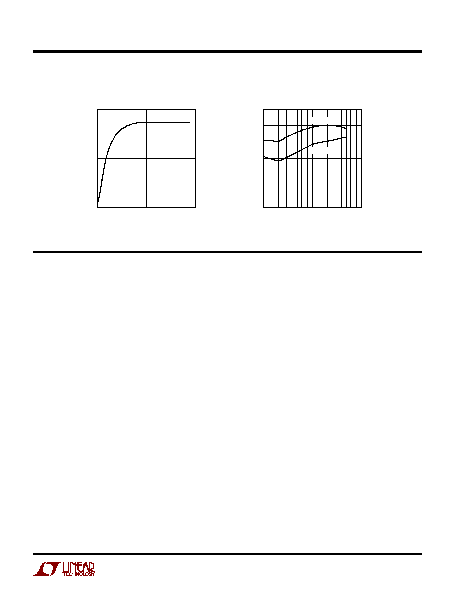
Auxiliary Regulator
Sink Current Available
AUX DR VOLTAGE (V)
0
0
AUX DR CURRENT (mA)
5
10
15
20
2
4
6
8
1436 G19
10
12
14
16
Auxiliary Regulator PSRR
FREQUENCY (kHz)
10
10
20
30
40
50
60
70
PSRR (dB)
100
1000
1436 G20
10mA LOAD
100mA LOAD
PI
N
FU
N
CTIO
N
S
U
U
U
V
IN
: Main Supply Pin. Must be closely decoupled to the
IC's signal ground pin.
INTV
CC
: Output of the Internal 5V Regulator and EXTV
CC
Switch. The driver and control circuits are powered from
this voltage. Must be closely decoupled to power ground
with a minimum of 2.2
µ
F tantalum or electrolytic capacitor.
DRV
CC
: Bottom MOSFET Driver Supply Voltage.
EXTV
CC
: Input to the Internal Switch Connected to INTV
CC
.
This switch closes and supplies V
CC
power whenever
EXTV
CC
is higher than 4.7V. See EXTV
CC
connection in
Applications Information section. Do not exceed 10V on
this pin. Connect to V
OUT
if V
OUT
5V.
BOOST: Supply to Topside Floating Driver. The bootstrap
capacitor is returned to this pin. Voltage swing at this pin
is from INTV
CC
to V
IN
+ INTV
CC
.
SW: Switch Node Connection to Inductor. Voltage swing
at this pin is from a Schottky diode (external) voltage drop
below ground to V
IN
.
SGND: Small Signal Ground. Must be routed separately
from other grounds to the (≠) terminal of C
OUT
.
PGND: Driver Power Ground. Connects to source of
bottom N-channel MOSFET and the (≠) terminal of C
IN
.
SENSE
≠
: The (≠) Input to the Current Comparator.
SENSE
+
: The (+) Input to the Current Comparator. Built-
in offsets between SENSE
≠
and SENSE
+
pins in conjunction
with R
SENSE
set the current trip thresholds.
V
OSENSE
: Receives the remotely sensed feedback voltage
either from the output or from an external resistive divider
across the output . The V
PROG
pin determines which point
V
OSENSE
must connect to.
V
PROG
: This voltage selects the output voltage. For V
PROG
< V
INTVCC
/3 the output is set to 3.3V with V
OSENSE
connected to the output. With V
PROG
> V
INTVCC
/1.5 the
output is set to 5V with V
OSENSE
connected to the output.
Leaving V
PROG
open (DC) allows the output voltage to be
set by an external resistive divider connected to V
OSENSE
.
C
OSC
: External capacitor C
OSC
from this pin to ground sets
the operating frequency.
I
TH
: Error Amplifier Compensation Point. The current
comparator threshold increases with this control voltage.
Nominal voltage range for this pin is 0V to 2.5V.
RUN/SS: Combination of Soft Start and Run Control
Inputs. A capacitor to ground at this pin sets the ramp time
to full current output. The time is approximately 0.5s/
µ
F.

8
LTC1436A
LTC1436-PLL-A/LTC1437A
PI
N
FU
N
CTIO
N
S
U
U
U
Forcing this pin below 1.3V causes the device to be shut
down. In shutdown all functions are disabled.
TGL: High Current Gate Drive for Main Top N-Channel
MOSFET. This is the output of a floating driver with a
voltage swing equal to INTV
CC
superimposed on the
switch node voltage SW.
TGS: High Current Gate Drive for a Small Top N-Channel
MOSFET. This is the output of a floating driver with a
voltage swing equal to INTV
CC
superimposed on the
switch node voltage SW. Leaving TGS open invokes Burst
Mode operation at low load currents.
BG: High Current Gate Drive for Bottom N-Channel
MOSFET. Voltage swing at this pin is from ground to
INTV
CC
(DRV
CC
).
SFB: Secondary Winding Feedback Input. Normally
connected to a feedback resistive divider from the
secondary winding. This pin should be tied to: ground to
force continuous operation; INTV
CC
in applications that
don't use a secondary winding; and a resistive divider from
the output in applications using a secondary winding.
POR: Open Drain Output of an N-Channel Pull-Down. This
pin sinks current when the output voltage is 7.5% out of
regulation and releases 65536 oscillator cycles after the
output voltage rises to ≠ 5% of its regulated value. The
POR output is asserted when Run/SS is low independent
of V
OUT
.
LBO: Open Drain Output of an N-Channel Pull-Down. This
pin will sink current when the LBI pin goes below 1.19V.
LBI: The (+) Input of the Low Battery Voltage Comparator.
The (≠) input is connected to a 1.19V reference.
PLLIN: External Synchronizing Input to Phase Detector.
This pin is internally terminated to SGND with 50k
. Tie
this pin to SGND in applications which do not use the
phase-locked loop.
PLL LPF: Output of Phase Detector and Control Input of
Oscillator. Normally a series RC lowpass filter network is
connected from this pin to ground. Tie this pin to SGND in
applications which do not use the phase-locked loop. Can
be driven by 0V to 2.4V logic signal for a frequency shifting
option.
AUXFB: Feedback Input to the Auxiliary Regulator/
Comparator. When used as a linear regulator, this input
can either be connected to an external resistive divider or
directly to the collector of the external PNP pass device for
12V operation. When used as a comparator, this is the
noninverting input of a comparator whose inverting input
is tied to the internal 1.19V reference. See Auxiliary
Regulator/Comparator in Applications Information section.
AUXON: Pulling this pin high turns on the auxiliary regulator/
comparator. The threshold is 1.19V.
AUXDR: Open Drain Output of the Auxiliary Regulator/
Comparator. The base of an external PNP device is
connected to this pin for use as a linear regulator. An
external pull-up resistor is required for use as a comparator.
A voltage > 9.5V on AUXDR causes the internal 12V
resistive divider to be connected to AUXFB.
9
LTC1436A
LTC1436A-PLL/LTC1437A
FU
N
CTIO
N
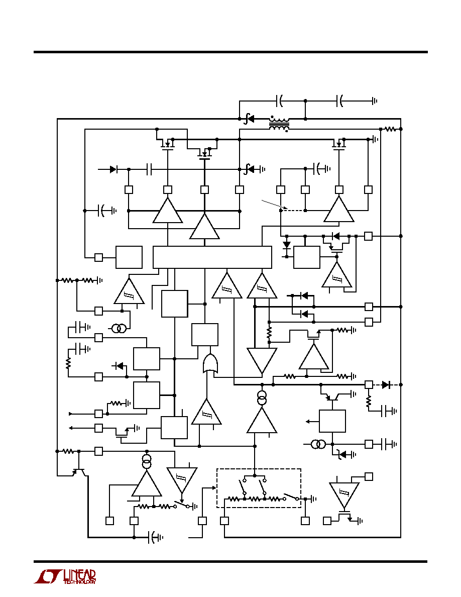
AL DIAGRA
U
U
W
≠
+
≠
+
≠
+
+
12V OUT
AUXON
AUXDR
POR
PLLIN*
PLL LPF*
2.4V
R
LP
C
OSC
SFB
1.10V
1.28V
V
FB
1.19V
320k
61k
119k
1.19V
RUN/SS
C
SS
C
C
OV
1.19V
0.6V
I2
4k
INTV
CC
V
IN
PGND
BG
DRV
CC
C
OUT
C
SEC
V
SEC
C
B
C
IN
V
IN
D
B
V
OUT
INTV
CC
C
INTVCC
SW
D1
1436 FD
TGS
TGL
M1
M3
M2
BOOST
SHUTDOWN
SHUTDOWN
1
µ
A
3
µ
A
6V
30k
180k
R
C
I
TH
D
FB
SENSE
+
EXTV
CC
CONNECTION FOR
LTC1436A/LTC1436A-PLL
SENSE
≠
8k
4.8V
AUXFB
INTV
CC
V
PROG
V
OSENSE
SGND
LBO**
LBI**
*
LTC1436A-PLL/LTC1437A ONLY
**
LTC1436A/LTC1437A ONLY
FOLDBACK CURRENT LIMITING
OPTION
1.19V
90.8k
10k
50k
9V
C
OUT2
≠
+
≠
+
AUX
PWR-ON
RESET
PHASE
DETECTOR
DROPOUT
DETECTOR
OSC
C
OSC
V
IN
INTV
CC
C
LP
S
R
Q
≠
+
≠
+
R
SENSE
1.19V
REF
SWITCH
LOGIC
≠
+
≠
+
I1
≠
+
≠
+
+
+
+
+
5V
LDO
REF
RUN/
SOFT
START
EA
g
m
= 1m

10
LTC1436A
LTC1436-PLL-A/LTC1437A
OPERATIO
U
(Refer to Functional Diagram)
Main Control Loop
The LTC1436A/LTC1437A use a constant frequency, cur-
rent mode step-down architecture. During normal opera-
tion, the top MOSFET is turned on each cycle when the
oscillator sets the RS latch and turned off when the main
current comparator I1 resets the RS latch. The peak
inductor current at which I1 resets the RS latch is con-
trolled by the voltage on I
TH
pin, which is the output of error
amplifier EA. V
PRGM
and V
OSENSE
pins, described in the Pin
Functions, allow EA to receive an output feedback voltage
V
FB
from either internal or external resistive dividers. When
the load current increases, it causes a slight decrease in
V
FB
relative to the 1.19V reference, which in turn causes the
I
TH
voltage to increase until the average inductor current
matches the new load current. While the top MOSFET is off,
the bottom MOSFET is turned on until either the inductor
current starts to reverse, as indicated by current compara-
tor I2, or the beginning of the next cycle.
The top MOSFET drivers are biased from floating boot-
strap capacitor C
B
, which normally is recharged during
each off cycle. However, when V
IN
decreases to a voltage
close to V
OUT
, the loop may enter dropout and attempt to
turn on the top MOSFET continuously. The dropout detec-
tor counts the number of oscillator cycles that the top
MOSFET remains on, and periodically forces a brief off
period to allow C
B
to recharge.
The main control loop is shut down by pulling RUN/SS pin
low. Releasing RUN/SS allows an internal 3
µ
A current
source to charge soft start capacitor C
SS
. When C
SS
reaches 1.3V, the main control loop is enabled with the I
TH
voltage clamped at approximately 30% of its maximum
value. As C
SS
continues to charge, I
TH
is gradually re-
leased allowing normal operation to resume.
Comparator OV guards against transient overshoots
> 7.5% by turning off the top MOSFET and keeping it off
until the fault is removed.
Low Current Operation
Adaptive Power mode allows the LTC1436A/LTC1437A to
automatically change between two output stages sized for
different load currents. TGL and BG pins drive large
synchronous N-channel MOSFETs for operation at high
currents, while the TGS pin drives a much smaller
N-channel MOSFET used in conjunction with a Schottky
diode for operation at low currents. This allows the loop to
continue to operate at normal frequency as the load
current decreases without incurring the large MOSFET
gate charge losses. If the TGS pin is left open, the loop
defaults to Burst Mode
operation in which the large
MOSFETs operate intermittently based on load demand.
Adaptive Power mode provides constant frequency opera-
tion down to approximately 1% of rated load current. This
results in an order of magnitude reduction of load current
before Burst Mode operation commences. Without the
small MOSFET (i.e.: no Adaptive Power mode), the transi-
tion to Burst Mode operation is approximately 10% of
rated load current.
The transition to low current operation begins when com-
parator I2 detects current reversal and turns off the
bottom MOSFET. If the voltage across R
SENSE
does not
exceed the hysteresis of I2 (approximately 20mV) for one
full cycle, then on following cycles the top drive is routed to
the small MOSFET at TGS pin and BG pin is disabled. This
continues until an inductor current peak exceeds 20mV/
R
SENSE
or the I
TH
voltage exceeds 0.6V, either of which
causes drive to be returned to TGL pin on the next cycle.
Two conditions can force continuous synchronous opera-
tion, even when the load current would otherwise dictate
low current operation. One is when the common mode
voltage of the SENSE
+
and SENSE
≠
pins is below 1.4V and
the other is when the SFB pin is below 1.19V. The latter
condition is used to assist in secondary winding regulation
as described in the Applications Information section.
Frequency Synchronization
A Phase-locked loop (PLL) is available on the
LTC1436A-PLL and LTC1437A to allow the oscillator to be
synchronized to an external source connected to the
PLLIN pin. The output of the phase detector at the PLL LPF
pin is also the control input of the oscillator, which
operates over a 0V to 2.4V range corresponding to ≠ 30%
to 30% in frequency. When locked, the PLL aligns the turn-
on of the top MOSFET to the rising edge of the synchroniz-
ing signal. When PLLIN is left open or at a constant DC
voltage, PLL LPF goes low, forcing the oscillator to mini-
mum frequency.

11
LTC1436A
LTC1436A-PLL/LTC1437A
OPERATIO
U
(Refer to Functional Diagram)
Power-On Reset
The POR pin is an open drain output which pulls low when
the main regulator output voltage is out of regulation.
When the output voltage rises to within 7.5% of regula-
tion, a timer is started which releases POR after 2
16
(65536) oscillator cycles. In shutdown, the POR output is
pulled low.
Auxiliary Linear Regulator
The auxiliary linear regulator in the LTC1436A/LTC1437A
controls an external PNP transistor for operation up to
500mA. An internal AUXFB resistive divider set for 12V
operation is invoked when AUXDR pin is above 9.5V to
allow 12V VPP supplies to be easily implemented. When
AUXDR is below 8.5V an external feedback divider may be
used to set other output voltages. Taking the AUXON pin
low shuts down the auxiliary regulator providing a conve-
nient logic controlled power supply.
The AUX block can be used as a comparator having its
inverting input tied to the internal 1.19V reference. The
AUXDR pin is used as the output and requires an external
pull-up to a supply less than 8.5V in order to inhibit the
invoking of the internal resistive divider.
INTV
CC
/DRV
CC
/EXTV
CC
Power
Power for the top and bottom MOSFET drivers and most
of the other LTC1436A/LTC1437A circuitry is derived from
the INTV
CC
pin. The bottom MOSFET driver supply DRV
CC
pin is internally connected to INTV
CC
in the LTC1436A and
externally connected to INTV
CC
in the LTC1437A. When
the EXTV
CC
pin is left open, an internal 5V low dropout
regulator supplies INTV
CC
power. If EXTV
CC
is taken above
4.8V, the 5V regulator is turned off and an internal switch
is turned on to connect EXTV
CC
to INTV
CC
. This allows the
INTV
CC
power to be derived from a high efficiency external
source such as the output of the regulator itself or a
secondary winding, as described in the Applications Infor-
mation section.
APPLICATIO
N
S I
N
FOR
M
ATIO
N
W
U
U
U
The basic LTC1436A application circuit is shown in Figure
1, High Efficiency Step-Down Converter. External compo-
nent selection is driven by the load requirement, and
begins with the selection of R
SENSE
. Once R
SENSE
is
known, C
OSC
and L can be chosen. Next, the power
MOSFETs and D1 are selected. Finally, C
IN
and C
OUT
are
selected. The circuit shown in Figure 1 can be configured
for operation up to an input voltage of 28V (limited by the
external MOSFETs).
R
SENSE
Selection For Output Current
R
SENSE
is chosen based on the required output current.
The LTC1436A/LTC1437A current comparator has a maxi-
mum threshold of 150mV/R
SENSE
and an input common
mode range of SGND to INTV
CC
. The current comparator
threshold sets the peak of the inductor current, yielding a
maximum average output current I
MAX
equal to the peak
value less half the peak-to-peak ripple current
I
L
.
Allowing a margin for variations in the LTC1436A/
LTC1437A and external component values yields:
R
mV
SENSE
MAX
=
100
I
The LTC1436A/LTC1437A work well with R
SENSE
values
0.005
.
C
OSC
Selection for Operating Frequency
The LTC1436A/LTC1437A use a constant frequency
architecture with the frequency determined by an external
oscillator capacitor C
OSC
. Each time the topside MOSFET
turns on, the voltage on C
OSC
is reset to ground. During the
on-time, C
OSC
is charged by a fixed current plus an
additional current which is proportional to the output
voltage of the phase detector V
PLLLPF
(LTC1436A-PLL/
LTC1437A). When the voltage on the capacitor reaches
1.19V, C
OSC
is reset to ground. The process then repeats.
The value of C
OSC
is calculated from the desired operating
frequency. Assuming the phase-locked loop has no exter-
nal oscillator input (V
PLLLPF
= 0V):
12
LTC1436A
LTC1436-PLL-A/LTC1437A
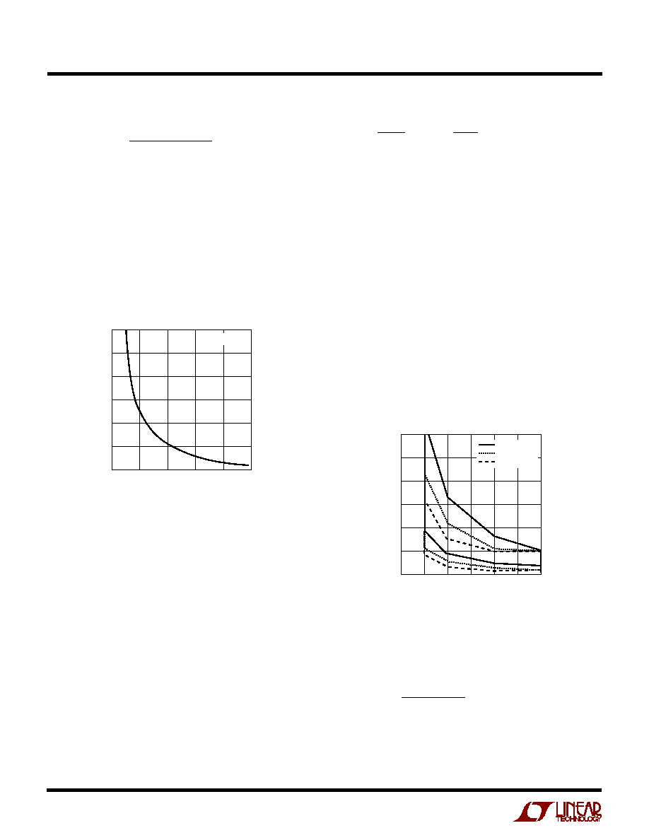
APPLICATIO
N
S I
N
FOR
M
ATIO
N
W
U
U
U
OPERATING FREQUENCY (kHz)
C
OSC
VALUE (pF)
300
250
200
150
100
50
0
100
200
300
400
1436 F02
500
0
V
PLLLPF
= 0V
Figure 2. Timing Capacitor Value
Inductor Value Calculation
The operating frequency and inductor selection are inter-
related in that higher operating frequencies allow the use
of smaller inductor and capacitor values. So why would
anyone ever choose to operate at lower frequencies with
larger components? The answer is efficiency. A higher
frequency generally results in lower efficiency because of
MOSFET gate charge losses. In addition to this basic
trade-off, the effect of inductor value on ripple current and
low current operation must also be considered.
The inductor value has a direct effect on ripple current. The
inductor ripple current
I
L
decreases with higher induc-
tance or frequency and increases with higher V
IN
or V
OUT
:
C
pF
Frequency kHz
OSC
( )
=
( )
1 37 10
11
4
.
(
)
≠
A graph for selecting C
OSC
vs frequency is given in Figure
2. As the operating frequency is increased the gate
charge losses will be higher, reducing efficiency (see
Efficiency Considerations). The maximum recommended
switching frequency is 400kHz. When using Figure 2 for
synchronizable applications, choose C
OSC
correspond-
ing to a frequency approximately 30% below your center
frequency. (See Phase-Locked Loop and Frequency Syn-
chronization.)
For low duty cycle, high frequency applications where the
required minimum on-time,
t
V
V
f
ON MIN
OUT
IN MAX
(
)
(
)
=
(
)( )
is less than 350ns, there may be further restrictions on the
inductance to ensure proper operation. See Minimum On-
Time Considerations section for more details.
OPERATING FREQUENCY (kHz)
0
INDUCTOR VALUE (
µ
H)
60
50
40
30
20
10
0
50
100
150
200
1436 F03
250
300
V
OUT
= 5V
V
OUT
= 3.3V
V
OUT
2.5V
Figure 3. Recommended Inductor Values
I
f L
V
V
V
L
OUT
OUT
IN
=
( )( )
-
1
1
Accepting larger values of
I
L
allows the use of low
inductances, but results in higher output voltage ripple
and greater core losses. A reasonable starting point for
setting ripple current is
I
L
= 0.4 (I
MAX
). Remember, the
maximum
I
L
occurs at the maximum input voltage.
The inductor value also has an effect on low current
operation. The transition to low current operation begins
when the inductor current reaches zero while the bottom
MOSFET is on. Lower inductor values (higher
I
L
) will
cause this to occur at higher load currents, which can
cause a dip in efficiency in the upper range of low current
operation. In Burst Mode operation (TGS pin open),
lower inductance values will cause the burst frequency to
decrease.
The Figure 3 graph gives a range of recommended induc-
tor values vs operating frequency and V
OUT
.

13
LTC1436A
LTC1436A-PLL/LTC1437A
APPLICATIO
N
S I
N
FOR
M
ATIO
N
W
U
U
U
frequency operation down to lower currents before cycle
skipping occurs.
The R
DS(ON)
recommended for the small MOSFET is
around 0.5
. Be careful not to use a MOSFET with an
R
DS(ON)
that is too low; remember, we want to conserve
gate charge. (A higher R
DS(ON)
MOSFET has a smaller gate
capacitance and thus requires less current to charge its
gate). For cost sensitive applications the small MOSFET
can be removed. The circuit will then begin Burst Mode
operation as the load current is dropped.
The peak-to-peak gate drive levels are set by the INTV
CC
voltage. This voltage is typically 5V during start-up (see
EXTV
CC
Pin Connection). Consequently, logic level
threshold MOSFETs must be used in most LTC1436A/
LTC1437A applications. The only exception is applications
in which EXTV
CC
is powered from an external supply
greater than 8V (must be less than 10V), in which standard
threshold MOSFETs [V
GS(TH)
< 4V] may be used. Pay close
attention to the BV
DSS
specification for the MOSFETs as
well; many of the logic level MOSFETs are limited to 30V
or less.
Selection criteria for the power MOSFETs include the "ON"
resistance R
SD(ON)
, reverse transfer capacitance C
RSS
,
input voltage and maximum output current. When the
LTC1436A/LTC1437A are operating in continuous mode
the duty cycles for the top and bottom MOSFETs are
given by:
Main Switch Duty Cycle =
V
V
OUT
IN
Synchronous Switch Duty Cycle =
V
IN
-
(
)
V
V
OUT
IN
Kool M
µ
is a registered trademark of Magnetics, Inc.
P
V
V
I
R
k V
I
C
f
P
V
V
V
I
R
MAIN
OUT
IN
MAX
DS ON
IN
MAX
RSS
SYNC
IN
OUT
IN
MAX
DS ON
=
( )
+
( )
+
( ) ( )( )( )
=
-
( )
+
( )
( )
( )
2
1 85
2
1
1
.
Inductor Core Selection
Once the value for L is known, the type of inductor must
be selected. High efficiency converters generally cannot
afford the core loss found in low cost powdered iron
cores, forcing the use of more expensive ferrite,
molypermalloy, or Kool M
µ
Æ
cores. Actual core loss is
independent of core size for a fixed inductor value, but it
is very dependent on inductance selected. As inductance
increases, core losses go down. Unfortunately, increased
inductance requires more turns of wire and therefore
copper losses will increase.
Ferrite designs have very low core loss and are prefered at
high switching frequencies, so design goals can concen-
trate on copper loss and preventing saturation. Ferrite
core material saturates "hard," which means that induc-
tance collapses abruptly when the peak design current is
exceeded. This results in an abrupt increase in inductor
ripple current and consequent output voltage ripple. Do
not allow the core to saturate!
Molypermalloy (from Magnetics, Inc.) is a very good, low
loss core material for toroids, but it is more expensive than
ferrite. A reasonable compromise from the same manu-
facturer is Kool M
µ
. Toroids are very space efficient,
especially when you can use several layers of wire.
Because they generally lack a bobbin, mounting is more
difficult. However, designs for surface mount are available
which do not increase the height significantly.
Power MOSFET and D1 Selection
Three external power MOSFETs must be selected for use
with the LTC1436A/LTC1437A: a pair of N-channel MOS-
FETs for the top (main) switch and an N-channel MOSFET
for the bottom (synchronous) switch.
To take advantage of the Adaptive Power output stage, two
topside MOSFETs must be selected. A large (low R
SD(ON)
)
MOSFET and a small (higher R
DS(ON)
) MOSFET are
required. The large MOSFET is used as the main switch
and works in conjunction with the synchronous switch.
The smaller MOSFET is only enabled under low load
current conditions. This increases midcurrent efficiencies
while continuing to operate at constant frequency. Also, by
using the small MOSFET the circuit can maintain constant
The MOSFET power dissipations at maximum output
current are given by:

14
LTC1436A
LTC1436-PLL-A/LTC1437A
APPLICATIO
N
S I
N
FOR
M
ATIO
N
W
U
U
U
This formula has a maximum at V
IN
= 2V
OUT
, where
I
RMS
= I
OUT
/2. This simple worst-case condition is com-
monly used for design because even significant deviations
do not offer much relief. Note that capacitor manufacturer's
ripple current ratings are often based on only 2000 hours
of life. This makes it advisable to further derate the
capacitor, or to choose a capacitor rated at a higher
temperature than required. Several capacitors may also be
paralleled to meet size or height requirements in the
design. Always consult the manufacturer if there is any
question.
The selection of C
OUT
is driven by the required effective
series resistance (ESR). Typically, once the ESR require-
ment is satisified, the capacitance is adequate for filtering.
The output ripple (
V
OUT
) is approximated by:
V
I ESR
fC
OUT
L
OUT
+
1
4
where f = operating frequency, C
OUT
= output capacitance
and
I
L
= ripple current in the inductor. The output ripple
is highest at maximum input voltage since
I
L
increases
with input voltage. With
I
L
= 0.4I
OUT(MAX)
the output
ripple will be less than 100mV at maximum V
IN
, assuming:
C
OUT
Required ESR < 2R
SENSE
Manufacturers such as Nichicon, United Chemicon and
Sanyo should be considered for high performance through-
hole capacitors. The OS-CON semiconductor dielectric
capacitor available from Sanyo has the lowest ESR (size)
product of any aluminum electrolytic at a somewhat
higher price. Once the ESR requirement for C
OUT
has been
met, the RMS current rating generally far exceeds the
I
RIPPLE(P-P)
requirement.
In surface mount applications multiple capacitors may
have to be paralleled to meet the ESR or RMS current
handling requirements of the application. Aluminum elec-
trolytic and dry tantalum capacitors are both available in
surface mount configurations. In the case of tantalum, it is
critical that the capacitors are surge tested for use in
switching power supplies. An excellent choice is the AVX
TPS series of surface mount tantalums, available in case
heights ranging from 2mm to 4mm. Other capacitor types
where
is the temperature dependency of R
DS(ON)
and k
is a constant inversely related to the gate drive current.
Both MOSFETs have I
2
R losses while the topside
N-channel equation includes an additional term for transi-
tion losses, which are highest at high input voltages. For
V
IN
< 20V the high current efficiency generally improves
with larger MOSFETs, while for V
IN
> 20V the transition
losses rapidly increase to the point that the use of a higher
R
DS(ON)
device with lower C
RSS
actual provides higher
efficiency. The synchronous MOSFET losses are greatest
at high input voltage or during a short circuit when the
duty cycle in this switch is nearly 100%. Refer to the
Foldback Current Limiting section for further applications
information.
The term (1 +
) is generally given for a MOSFET in the
form of a normalized R
DS(ON)
vs temperature curve, but
= 0.005/
∞
C can be used as an approximation for low
voltage MOSFETs. C
RSS
is usually specified in the MOSFET
characteristics. The constant k = 2.5 can be used to
estimate the contributions of the two terms in the main
switch dissipation equation.
The Schottky diode D1 shown in Figure 1 serves two
purposes. During continuous synchronous operation, D1
conducts during the dead-time between the conduction of
the two large power MOSFETs. This prevents the body
diode of the bottom MOSFET from turning on and storing
charge during the dead-time, which could cost as much as
1% in efficiency. During low current operation, D1 oper-
ates in conjunction with the small top MOSFET to provide
an efficient low current output stage. A 1A Schottky is
generally a good compromise for both regions of opera-
tion due to the relatively small average current.
C
IN
and C
OUT
Selection
In continuous mode, the source current of the top
N-channel MOSFET is a square wave of duty cycle V
OUT
/
V
IN
. To prevent large voltage transients, a low ESR input
capacitor sized for the maximum RMS current must be
used. The maximum RMS capacitor current is given by:
C
I
V
V
V
V
IN
MAX
OUT
IN
OUT
IN
Required I
RMS
-
(
)
[
]
1 2
/
15
LTC1436A
LTC1436A-PLL/LTC1437A
APPLICATIO
N
S I
N
FOR
M
ATIO
N
W
U
U
U
include Sanyo OS-CON, Nichicon PL series and Sprague
593D and 595D series. Consult the manufacturer for other
specific recommendations.
INTV
CC
Regulator
An internal P-channel low dropout regulator produces the
5V supply that powers the drivers and internal circuitry
within the LTC1436A/LTC1437A. The INTV
CC
pin can
supply up to 15mA and must be bypassed to ground with
a minimum of 2.2
µ
F tantalum or low ESR electrolytic.
Good bypassing is necessary to supply the high transient
currents required by the MOSFET gate drivers.
High input voltage applications, in which large MOSFETs
are being driven at high frequencies, may cause the
maximum junction temperature rating for the LTC1436A/
LTC1437A to be exceeded. The IC supply current is
dominated by the gate charge supply current when not
using an output derived EXTV
CC
source. The gate charge
is dependent on operating frequency as discussed in the
Efficiency Considerations section. The junction tempera-
ture can be estimated by using the equations given in Note
1 of the Electrical Characteristics. For example, the
LTC1437A is limited to less than 19mA from a 30V supply:
T
V
C W
C
J
= 70 C + 19mA
∞
( )( )
∞
(
)
=
∞
30
95
124
/
To prevent maximum junction temperature from being
exceeded, the input supply current must be checked when
operating in continuous mode at maximum V
IN
.
EXTV
CC
Connection
The LTC1436A/LTC1437A contain an internal P-channel
MOSFET switch connected between the EXTV
CC
and
INTV
CC
pins. The switch closes and supplies the INTV
CC
power whenever the EXTV
CC
pin is above 4.8V, and
remains closed until EXTV
CC
drops below 4.5V. This
allows the MOSFET driver and control power to be derived
from the output during normal operation (4.8V < V
OUT
<
9V) and from the internal regulator when the output is out
of regulation (start-up, short circuit). Do not apply greater
than 10V to the EXTV
CC
pin and ensure that EXTV
CC
< V
IN
.
Significant efficiency gains can be realized by powering
INTV
CC
from the output, since the V
IN
current resulting
from the driver and control currents will be scaled by a
factor of Duty Cycle
/
Efficiency. For 5V regulators this
supply means connecting the EXTV
CC
pin directly to V
OUT
.
However, for 3.3V and other lower voltage regulators,
additional circuitry is required to derive INTV
CC
power
from the output.
The following list summarizes the four possible connec-
tions for EXTV
CC
:
1. EXTV
CC
left open (or grounded). This will cause INTV
CC
to be powered from the internal 5V regulator resulting
in an efficiency penalty of up to 10% at high input
voltages.
2. EXTV
CC
connected directly to V
OUT
. This is the normal
connection for a 5V regulator and provides the highest
efficiency.
3. EXTV
CC
connected to an output-derived boost network.
For 3.3V and other low voltage regulators, efficiency
gains can still be realized by connecting EXTV
CC
to an
output-derived voltage which has been boosted to
greater than 4.8V. This can be done with either the
inductive boost winding as shown in Figure 4a or the
capacitive charge pump shown in Figure 4b. The charge
pump has the advantage of simple magnetics.
4. EXTV
CC
connected to an external supply. If an external
supply is available in the 5V to 10V range (EXTV
CC
<
V
IN
), it may be used to power EXTV
CC
, providing it is
compatible with the MOSFET gate drive requirements.
When driving standard threshold MOSFETs, the exter-
nal supply must always be present during operation to
prevent MOSFET failure due to insufficient gate drive.
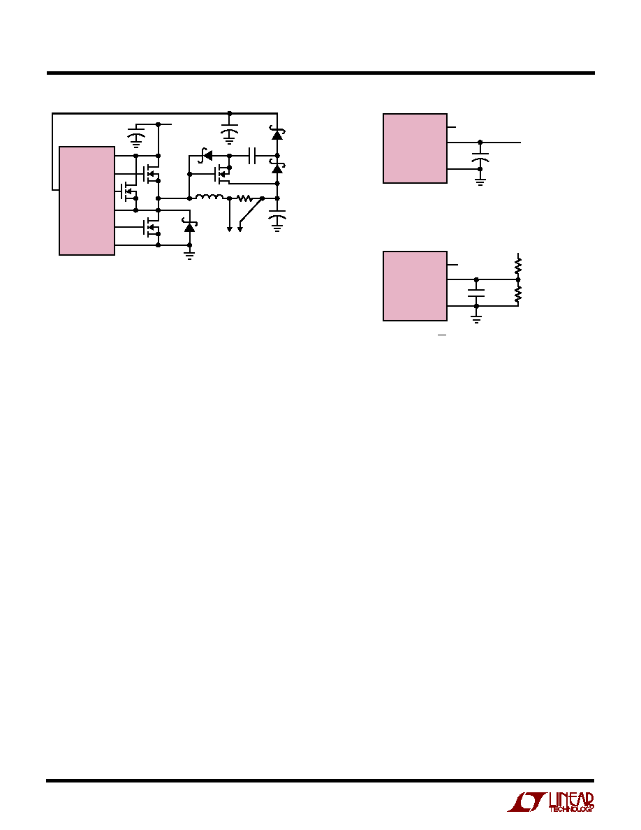
Figure 4a. Secondary Output Loop and EXTV
CC
Connection
R6
R5
EXTV
CC
V
IN
TGL
TGS
SW
BG
PGND
LTC1436A
LTC1437A
N-CH
N-CH
N-CH
+
C
IN
V
IN
1N4148
+
1
µ
F
+
C
OUT
V
SEC
T1
1:N
R
SENSE
V
OUT
OPTIONAL EXTV
CC
CONNECTION
5V
V
SEC
9V
1436 F04a
SFB
SGND
16
LTC1436A
LTC1436-PLL-A/LTC1437A
APPLICATIO
N
S I
N
FOR
M
ATIO
N
W
U
U
U
Topside MOSFET Driver Supply (C
B
, D
B
)
An external bootstrap capacitor C
B
connected to the Boost
pin supplies the gate drive voltage for the topside
MOSFET(s). Capacitor C
B
in the functional diagram is
charged through diode D
B
from INTV
CC
when the SW pin
is low. When one of the topside MOSFET(s) is to be turned
on, the driver places the C
B
voltage across the gate source
of the desired MOSFET. This enhances the MOSFET and
turns on the topside switch. The switch node voltage SW
rises to V
IN
and the Boost pin rises to V
IN
+ INTV
CC
. The
value of the boost capacitor C
B
needs to be 100 times
greater than the total input capacitance of the topside
MOSFET(s). In most applications 0.1
µ
F is adequate. The
reverse breakdown on D
B
must be greater than V
IN(MAX).
Output Voltage Programming
The output voltage is pin selectable for all members of the
LTC1436A/LTC1437A family. The output voltage is
selected by the V
PROG
pin as follows:
V
PROG
= 0V
V
OUT
= 3.3V
V
PROG
= INTV
CC
V
OUT
= 5V
V
PROG
= Open (DC)
V
OUT
= Adjustable
The LTC1436A/LTC1437A family also has remote output
voltage sense capability. The top of an internal resistive
divider is connected to V
OSENSE
. For fixed 3.3V and 5V
output voltage applications the V
OSENSE
pin is connected
to the output voltage as shown in Figure 5a. When using
an external resistive divider, the V
PROG
pin is left open (DC)
and the V
OSENSE
pin is connected to the feedback resistors
as shown in Figure 5b.
Figure 4b. Capacitive Charge Pump for EXT V
CC
Figure 5b. LTC1436A/LTC1437A Adjustable Applications
Figure 5a. LTC1436A/LTC1437A Fixed Output Applications
Power-On Reset Function (POR)
The power-on reset function monitors the output voltage
and turns on an open drain device when it is out of
regulation. An external pull-up resistor is required on the
POR pin.
When power is first applied or when coming out of
shutdown, the POR output is pulled to ground. When the
output voltage rises above a level which is 5% below the
final regulated output value, an internal counter starts.
After counting 2
16
(65536) clock cycles, the POR pull-
down device turns off.
The POR output will go low whenever the output voltage
drops below 7.5% of its regulated value for longer than
approximately 30
µ
s, signaling an out-of-regulation condi-
tion. In shutdown, the POR output is pulled low even if the
regulator's output is held up by an external source.
Run/Soft Start Function
The RUN/SS pin is a dual purpose pin that provides the
soft start function and a means to shut down the
LTC1436A/LTC1437A. Soft start reduces surge currents
from V
IN
by gradually increasing the internal current limit.
Power supply sequencing can also be accomplished
using this pin.
EXTV
CC
V
IN
TGL
TGS
SW
BG
PGND
LTC1436A
LTC1437A
N-CH
N-CH
N-CH
+
C
IN
V
IN
0.22
µ
F
BAT85
BAT85
C
OUT
BAT85
+
1
µ
F
+
L1
R
SENSE
VN2222LL
1436 F04b
V
PROG
SGND
LTC1436A
LTC1437A
1436 F05a
C
OUT
V
OUT
GND: V
OUT
= 3.3V
INTV
CC
: V
OUT
= 5V
+
V
OSENSE
R1
R2
OPEN (DC)
1436 F05b
100pF
1.19V
V
OUT
9V
V
PROG
SGND
LTC1436A
LTC1437A
V
OSENSE
V
OUT
= 1.19V 1 +
R2
R1
( )
17
LTC1436A
LTC1436A-PLL/LTC1437A
APPLICATIO
N
S I
N
FOR
M
ATIO
N
W
U
U
U
An internal 3
µ
A current source charges up an external
capacitor C
SS.
When the voltage on RUN/SS reaches 1.3V
the LTC1436A/LTC1437A begin operating. As the voltage
on RUN/SS continues to ramp from 1.3V to 2.4V, the
internal current limit is also ramped at a proportional linear
rate. The current limit begins at approximately 50mV/
R
SENSE
(at V
RUN/SS
= 1.3V) and ends at 150mV/R
SENSE
(V
RUN/SS
> 2.7V). The output current thus ramps up
slowly, charging the output capacitor. If RUN/SS has been
pulled all the way to ground there is a delay before starting
of approximately 500ms/
µ
F, followed by an additional
500ms/
µ
F to reach full current.
t
DELAY
= 5(10
5
)C
SS
seconds
Pulling the RUN/SS pin below 1.3V puts the LTC1436A/
LTC1437A into a low quiescent current shutdown (I
Q
<
25
µ
A). This pin can be driven directly from logic as shown
in Figure 6. Diode D1 in Figure 6 reduces the start delay but
allows C
SS
to ramp up slowly for the soft start function;
this diode and C
SS
can be deleted if soft start is not needed.
The RUN/SS pin has an internal 6V Zener clamp (see
Functional Diagram).
Foldback current limiting is implemented by adding a
diode D
FB
between the output and I
TH
pins as shown in the
Function Diagram. In a hard short (V
OUT
= 0V), the current
will be reduced to approximately 25% of the maximum
output current. This technique may be used for all applica-
tions with regulated output voltages of 1.8V or greater.
Phase-Locked Loop and Frequency Synchronization
The LTC1436A-PLL/LTC1437A each have an internal volt-
age-controlled oscillator and phase detector comprising a
phase-locked loop. This allows the top MOSFET turn-on to
be locked to the rising edge of an external source. The
frequency range of the voltage-controlled oscillator is
±
30% around the center frequency f
O
.
The value of C
OSC
is calculated from the desired operating
frequency f
O
. Assuming the phase-locked loop is
locked
(V
PLLLPF
= 1.19V):
C
Frequency
OSC
pF
kHz
( )
=
( )
2 1 10
11
4
. (
)
≠
Stating the frequency as a function of V
PLLLPF
and C
OSC
:
Frequency kHz
C
pF
A
A
V
V
OSC
PLLLPF
( )
=
( )
+
[
]
+
+
8 4 10
11
1
17
18
2 4
2000
8
. (
)
.
µ
µ
The phase detector used is an edge sensitive digital type
which provides zero degrees phase shift between the
external and internal oscillators. This type of phase detec-
tor will not lock up on input frequencies close to the
harmonics of the VCO center frequency. The PLL hold-in
range
f
H
is equal to the capture range:
f
H
=
f
C
=
±
0.3f
O
.
Foldback Current Limiting
As described in Power MOSFET and D1 Selection, the
worst-case dissipation for either MOSFET occurs with a
short-circuited output, when the synchronous MOSFET
conducts the current limit value almost continuously. In
most applications this will not cause excessive heating,
even for extended fault intervals. However, when heat
sinking is at a premium or higher R
DS(ON)
MOSFETs are
being used, foldback current limiting should be added to
reduce the current in proportion to the severity of the fault.
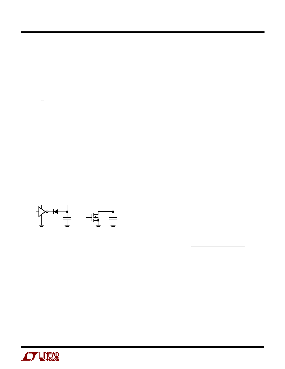
1436 F06
C
SS
D1
3.3V OR 5V
RUN/SS
C
SS
RUN/SS
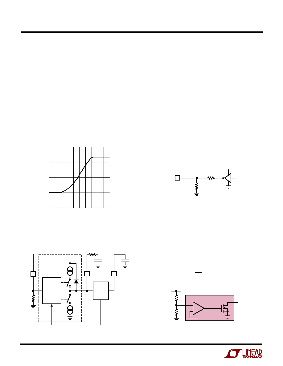
Figure 6. Run/SS Pin Interfacing
18
LTC1436A
LTC1436-PLL-A/LTC1437A
APPLICATIO
N
S I
N
FOR
M
ATIO
N
W
U
U
U
difference. Thus the voltage on the PLL LPF pin is adjusted
until the phase and frequency of the external and internal
oscillators are identical. At this stable operating point the
phase comparator output is open and the filter capacitor
C
LP
holds the voltage.
The loop filter components C
LP
and R
LP
smooth out the
current pulses from the phase detector and provide a
stable input to the voltage-controlled oscillator. The filter
components C
LP
and R
LP
determine how fast the loop
acquires lock. Typically, R
LP
= 10k and C
LP
is 0.01
µ
F to
0.1
µ
F. Be sure to connect the low side of the filter to SGND.
The PLL LPF pin can be driven with external logic to obtain
a 1:1.9 frequency shift. The circuit shown in Figure 9 will
provide a frequency shift from f
O
to 1.9f
O
as the voltage
and V
PLLLPF
increases from 0V to 2.4V. Do not exceed 2.4V
on V
PLLLPF
.
The output of the phase detector is a complementary pair
of current sources charging or discharging the external
filter network on the PLL LPF pin. The relationship
between the PLL LPF pin and operating frequency is
shown in Figure 7. A simplified block diagram is shown in
Figure 8.
If the external frequency (f
PLLIN
) is greater than the oscil-
lator frequency (f), current is sourced continuously, pull-
ing up the PLL LPF pin. When the external frequency is less
than f
OSC
, current is sunk continuously, pulling down the
PLL LPF pin. If the external and internal frequencies are the
same but exhibit a phase difference, the current sources
turn on for an amount of time corresponding to the phase
Figure 7. Operating Frequency vs V
PLLLPF
PLL LPF
2.4V MAX
3.3V OR 5V
1436 F09
18k
Figure 9. Directly Driving PLL LPF Pin
Low-Battery Comparator
The LTC1436A/LTC1437A have an on-chip low-battery
comparator which can be used to sense a low-battery
condition when implemented as shown in Figure 10. The
resistive divider R3, R4 sets the comparator trip point as
follows:
V
V
R
R
LBTRIP
=
+
1 19
1
4
3
.
PLLIN
50k
1436 F08
PLL LPF
C
OSC
PHASE
DETECTOR
OSC
R
LP
C
LP
C
OSC
EXTERNAL
FREQUENCY
2.4V
DIGITAL
PHASE/
FREQUENCY
DETECTOR
V
PLLLPF
(V)
0
FREQUENCY (kHz)
1.3f
O
0.7f
O
1436 F07
1.5
2.0
1.0
0.5
2.5
f
O
Figure 8. Phase-Locked Loop Block Diagram
Figure 10. Low Battery Comparator
≠
+
LBI
V
IN
SGND
LBO
R4
R3
1436 F10
1.19V REFERENCE
LTC1436A
LTC1437A

19
LTC1436A
LTC1436A-PLL/LTC1437A
APPLICATIO
N
S I
N
FOR
M
ATIO
N
W
U
U
U
The divided down voltage at the negative (≠) input to the
comparator is compared to an internal 1.19V reference. A
20mV hysteresis is built in to assure rapid switching. The
output is an open drain MOSFET and requires a pull-up
resistor. This comparator is
not active in shutdown. The
low side of the resistive divider should connect to SGND.
SFB Pin Operation
When the SFB pin drops below its ground-referenced
1.19V threshold, continuous mode operation is forced. In
continuous mode, the large N-channel main and synchro-
nous switches are used regardless of the load on the main
output.
In addition to providing a logic input to force continuous
synchronous operation, the SFB pin provides a means to
regulate a flyback winding output. Continuous synchro-
nous operation allows power to be drawn from the auxil-
iary windings without regard to the primary output load.
The SFB pin provides a way to force continuous synchro-
nous operation as needed by the flyback winding.
The secondary output voltage is set by the turns ratio of
the transformer in conjunction with a pair of external
resistors returned to the SFB pin as shown in Figure 4a.
The secondary regulated voltage V
SEC
in Figure 4a is
given by:
V
N
V
V
R
R
SEC
OUT
+
( )
>
+
1
1 19
1
6
5
.
where N is the turns ratio of the transformer and V
OUT
is
the main output voltage sensed by V
OSENSE
.
Auxiliary Regulator/Comparator
The auxiliary regulator/comparator can be used as a
comparator or low dropout regulator (by adding an exter-
nal PNP pass device).
When the voltage present at the AUXON pin is greater than
1.19V the regulator/comparator is on. Special circuitry
consumes a small (20
µ
A) bias current while still remain-
ing stable when operating as a low dropout regulator. No
excess current is drawn when the input stage is overdriven
when used as a comparator.
The AUXDR pin is internally connected to an open drain
MOSFET which can sink up to 10mA. The voltage on
AUXDR determines whether or not an internal 12V resis-
tive divider is connected to AUXFB as described below. A
pull-up resistor is required on AUXDR and the voltage
must not exceed 28V.
With the addition of an external PNP pass device, a linear
regulator capable of supplying up to 0.5A is created. As
shown in Figure 12a, the base of the external PNP con-
nects to the AUXDR pin together with a pull-up resistor.
The output voltage V
OAUX
at the collector of the external
PNP is sensed by the AUXFB pin.
The input voltage to the auxiliary regulator can be taken
from a secondary winding on the primary inductor as
shown in Figure 11a. In this application, the SFB pin
regulates the input voltage to the PNP regulator (see SFB
Pin Operation) and should be set to approximately 1V to
2V above the required output voltage of the auxiliary
regulator. A Zener diode clamp may be required to keep
V
SEC
under the 28V AUXDR pin specification when the
primary is heavily loaded and the secondary is not.
The AUXFB pin is the feedback point of the regulator. An
internal resistive divider is available to provide a 12V
output by simply connecting AUXFB directly to the collec-
tor of the external PNP. The internal resistive divider is
selected when the voltage at AUXFB goes above 9.5V with
1V built-in hysteresis. For other output voltages, an exter-
nal resistive divider is fed back to AUXFB as shown in
Figure 11b. The output voltage V
OAUX
is set as follows:
V
OAUX
= 1.19V(1+R8/R7) < 8V
AUXDR < 8.5V
V
OAUX
= 12V
AUXDR > 12V
The circuit can also be used as a noninverting voltage
comparator as shown in Figure 11c. When AUXFB drops
below 1.19V, the AUXDR pin will be pulled low. A mini-
mum current of 5
µ
A is required to pull the AUXDR pin to
5V when used as a comparator output, in order to coun-
teract a 1.5
µ
A internal current source.
20
LTC1436A
LTC1436-PLL-A/LTC1437A
APPLICATIO
N
S I
N
FOR
M
ATIO
N
W
U
U
U
Figure 11a. 12V Output Auxiliary Regulator Using
Internal Feedback Resistors
The minimum on-time for the LTC1436A/LTC1437A in a
properly configured application is less than 300ns but
increases at low ripple current amplitudes (see Figure 12).
If an application is expected to operate close to the
minimum on-time limit, an inductor value must be chosen
that is low enough to provide sufficient ripple amplitude to
meet the minimum on-time requirement. To determine the
proper value, use the following procedure:
1. Calculate on-time at maximum supply, t
ON(MIN)
=
(1/f)(V
OUT
/V
IN(MAX)
).
2. Use Figure 12 to obtain the peak-to-peak inductor ripple
current as a percentage of I
MAX
necessary to achieve
the calculated t
ON(MIN)
.
3. Ripple amplitude
I
L(MIN)
= (% from Figure 12) (I
MAX
)
where I
MAX
= 0.1/R
SENSE
.
4. L
MAX
= t
V
V
I
ON MIN
IN MAX
OUT
L MIN
(
)
(
)
(
)
≠
Choose an inductor less than or equal to the calculated
L
MAX
to ensure proper operation.
1436 F11a
V
SEC
= 1.19V 1 + > 13V
R6
R5
( )
ON/OFF
V
SEC
SECONDARY WINDING
R6
R5
10
µ
F
1:N
V
OAUX
12V
AUXDR
LTC1436A
LTC1437A
AUXFB
AUXON
+
SFB
+
Figure 11c. Auxiliary Comparator Configuration
≠
+
AUXON
AUXFB
ON/OFF
INPUT
V
PULL-UP
<
8.5V
AUXDR
OUTPUT
1436 F11c
1.19V REFERENCE
LTC1436A
LTC1437A
Figure 11b. 5V Output Auxiliary Regulator Using
External Feedback Resistors
ON/OFF
V
SEC
SECONDARY WINDING
R6
R5
R8
R7
1436 F11b
10
µ
F
1:N
V
OAUX
AUXDR
LTC1436A
LTC1437A
AUXFB
AUXON
V
SEC
= 1.19V 1 +
R6
R5
( )
V
OAUX
= 1.19V 1 +
R8
R7
( )
+
SFB
+
Minimum On-Time Considerations
Minimum on-time, t
ON(MIN)
, is the smallest amount of
time that the LTC1436A/LTC1437A are capable of turning
the top MOSFET on and off again. It is determined by
internal timing delays and the gate charge required to turn
on the top MOSFET. Low duty cycle applications may
approach this minimum on-time limit. If the duty cycle
falls below what can be accommodated by the minimum
on-time, the LTC1436A/LTC1437A will begin to skip cycles.
The output voltage will continue to be regulated, but the
ripple current and ripple voltage will increase. Therefore
this limit should be avoided.
Figure 12. Minimum On-Time vs Inductor Ripple Current
Because of the sensitivity of the LTC1436A/LTC1437A
current comparator when operating close to the minimum
on-time limit, it is important to prevent stray magnetic flux
generated by the inductor from inducing noise on the
current sense resistor, which may occur when axial type
cores are used. By orienting the sense resistor on the
radial axis of the inductor (see Figure 13), this noise will be
minimized.
INDUCTOR RIPPLE CURRENT (% OF I
MAX
)
0
200
MINIMUM ON-TIME (ns) 250
300
350
400
RECOMMENDED
REGION FOR MIN
ON-TIME AND
MAX EFFICIENCY
10
20
30
40
1435A F12
50
60
70

21
LTC1436A
LTC1436A-PLL/LTC1437A
APPLICATIO
N
S I
N
FOR
M
ATIO
N
W
U
U
U
Efficiency. For example, in a 20V to 5V application,
10mA of INTV
CC
current results in approximately 3mA
of V
IN
current. This reduces the midcurrent loss from
10% or more (if the driver was powered directly from
V
IN
) to only a few percent.
3. I
2
R losses are predicted from the DC resistances of the
MOSFET, inductor and current shunt. In continuous
mode the average output current flows through L and
R
SENSE
, but is "chopped" between the topside main
MOSFET and the synchronous MOSFET. If the two
MOSFETs have approximately the same R
DS(ON)
, then
the resistance of one MOSFET can simply be summed
with the resistances of L and R
SENSE
to obtain I
2
R
losses. For example, if each R
DS(ON)
= 0.05
,
R
L
= 0.15
and R
SENSE
= 0.05
, then the total resis-
tance is 0.25
. This results in losses ranging from 3%
to 10% as the output current increases from 0.5A to 2A.
I
2
R losses cause the efficiency to drop at high output
currents.
4. Transition losses apply only to the topside MOSFET(s),
and only when operating at high input voltages (typi-
cally 20V or greater). Transition losses can be esti-
mated from:
Transition Loss = 2.5(V
IN
)
1.85
(I
MAX
)(C
RSS
)(f)
Other losses including C
IN
and C
OUT
ESR dissipative
losses, Schottky conduction losses during dead-time and
inductor core losses, generally account for less than 2%
total additional loss.
Checking Transient Response
The regulator loop response can be checked by looking at
the load transient response. Switching regulators take
several cycles to respond to a step in DC (resistive) load
current. When a load step occurs, V
OUT
immediately shifts
by an amount equal to (
I
LOAD
)(ESR), where ESR is the
effective series resistance of C
OUT
.
I
LOAD
also begins to
charge or discharge C
OUT
which generates a feedback
error signal. The regulator loop then acts to return V
OUT
to
its steady-state value. During this recovery time V
OUT
can
be monitored for overshoot or ringing, which would
indicate a stability problem. The I
TH
external components
shown in the Figure 1 circuit will provide adequate com-
pensation for most applications.
L
INDUCTOR
1435A F08
Figure 13. Allowable Inductor/R
SENSE
Layout Orientations
Efficiency Considerations
The efficiency of a switching regulator is equal to the
output power divided by the input power times 100%. It is
often useful to analyze individual losses to determine what
is limiting the efficiency and which change would produce
the most improvement. Efficiency can be expressed as:
Efficiency = 100% ≠ (L1 + L2 + L3 + ...)
where L1, L2, etc. are the individual losses as a percentage
of input power.
Although all dissipative elements in the circuit produce
losses, four main sources usually account for most of the
losses in LTC1436A/LTC1437A circuits: LTC1436A/
LTC1437A V
IN
current, INTV
CC
current, I
2
R losses and
topside MOSFET transition losses.
1. The V
IN
current is the DC supply current given in the
Electrical Characteristics table which excludes MOSFET
driver and control currents. V
IN
current results in a
small (< 1%) loss which increases with V
IN
.
2. INTV
CC
current is the sum of the MOSFET driver and
control currents. The MOSFET driver current results
from switching the gate capacitance of the power
MOSFETs. Each time a MOSFET gate is switched from
low to high to low again, a packet of charge dQ moves
from INTV
CC
to ground. The resulting dQ/dt is a current
out of INTV
CC
that is typically much larger than the
control circuit current. In continuous mode, I
GATECHG
=
f(Q
T
+ Q
B
), where Q
T
and Q
B
are the gate charges of the
topside and bottom side MOSFETs. It is for this reason
that the Adaptive Power output stage switches to a low
Q
T
MOSFET during low current operation.
By powering EXTV
CC
from an output-derived source,
the additional V
IN
current resulting from the driver and
control currents will be scaled by a factor of Duty Cycle/
22
LTC1436A
LTC1436-PLL-A/LTC1437A
APPLICATIO
N
S I
N
FOR
M
ATIO
N
W
U
U
U
A second, more severe transient is caused by switching in
loads with large (>1
µ
F) supply bypass capacitors. The
discharged bypass capacitors are effectively put in parallel
with C
OUT
, causing a rapid drop in V
OUT
. No regulator can
deliver enough current to prevent this problem if the load
switch resistance is low and it is driven quickly. The only
solution is to limit the rise time of the switch drive so that
the load rise time is limited to approximately 25(C
LOAD
).
Thus a 10
µ
F capacitor would require a 250
µ
s rise time,
limiting the charging current to about 200mA.
Automotive Considerations: Plugging into the
Cigarette Lighter
As battery-powered devices go mobile, there is a natural
interest in plugging into the cigarette lighter in order to
conserve or even recharge battery packs during operation.
But before you connect, be advised: you are plugging into
the supply from hell. The main battery line in an automo-
bile is the source of a number of nasty potential transients,
including load dump, reverse battery, and double battery.
Load dump is the result of a loose battery cable. When the
cable breaks connection, the field collapse in the alternator
can cause a positive spike as high as 60V which takes
several hundred milliseconds to decay. Reverse battery is
just what it says, while double battery is a consequence of
tow-truck operators finding that a 24V jump start cranks
cold engines faster than 12V.
The network shown in Figure 14 is the most straightfor-
ward approach to protect a DC/DC converter from the
ravages of an automotive battery line. The series diode
prevents current from flowing during reverse battery,
while the transient suppressor clamps the input voltage
during load dump. Note that the transient suppressor
should not conduct during double battery operation, but
must still clamp the input voltage below breakdown of the
converter. Although the LTC1436A/LTC1437A have a maxi-
mum input voltage of 36V, most applications will be
limited to 30V by the MOSFET BV
DSS
.
Design Example
As a design example, assume V
IN
= 12V (nominal), V
IN
=
22V (max), V
OUT
= 1.6V, I
MAX
= 3A and f = 250kHz, R
SENSE
and C
OSC
can immediately be calculated:
R
mV
A
C
pF
SENSE
OSC
=
=
=
=
100
3
0 033
1 37 10
250
11 43
4
.
.
(
)
≠
Refering to Figure 3, a 4.7
µ
H inductor falls within the
recommended range. To check the actual value of the
ripple current the following equation is used:
I
V
f L
V
V
L
OUT
OUT
IN
=
( )( )
-
1
The highest value of the ripple current occurs at the
maximum input voltage:
I
V
kHz
H
V
V
A
L
=
( )
-
=
1 6
250
4 7
1
1 6
22
1 3
.
.
.
.
µ
The lowest duty cycle also occurs at maximum input
voltage. The on-time during this condition should be
checked to make sure it doesn't violate the LTC1436A/
LTC1437A's minimum on-time and cause cycle skipping
to occur. The required on-time at V
IN(MAX)
is:
t
V
V
f
V
V
kHz
ns
ON MIN
OUT
IN MAX
(
)
(
)
.
=
(
)
( )
=
( )(
)
=
1 6
22
250
291
The
I
L
was previously calculated to be 1.3A, which is
43% of I
MAX
. From Figure 12, the LTC1436A/LTC1437A's
minimum on-time at 43% ripple is about 235ns. There-
fore, the minimum on-time is sufficient and no cycle
skipping will occur.
Figure 14. Automotive Application Protection
1436 F14
50A IPK RATING
LTC1436A
LTC1437A
TRANSIENT VOLTAGE
SUPPRESSOR
GENERAL INSTRUMENT
1.5KA24A
V
IN
12V

23
LTC1436A
LTC1436A-PLL/LTC1437A
APPLICATIO
N
S I
N
FOR
M
ATIO
N
W
U
U
U
The power dissipation on the topside MOSFET can be
easily estimated. Choosing a Siliconix Si4412DY results
in: R
DS(ON)
= 0.042
, C
RSS
= 100pF. At maximum input
voltage with T (estimated) = 50
∞
C:
P
V
V
C
C
V
A
pF
kHz
mW
MAIN
=
( )
+
(
)
∞ - ∞
(
)
[
]
(
)
+
( ) ( )(
)(
)
=
1 6
22
3
1
0 005 50
25
0 042
2 5 22
3
100
250
88
2
1 85
.
.
.
.
.
The most stringent requirement for the synchronous
N-channel MOSFET occurs when V
OUT
= 0 (i.e. short
circuit). In this case the worst-case dissipation rises to:
P
I
R
SYNC
SC AVG
DS ON
=
+
( )
( )
( )
2
1
With the 0.033
sense resistor I
SC(AVG)
= 4A will result,
increasing the Si4412DY dissipation to 950mW at a die
temperature of 105
∞
C.
C
IN
is chosen for an RMS current rating of at least 1.5A at
temperature. C
OUT
is chosen with an ESR of 0.03
for low
output ripple. The output ripple in continuous mode will be
highest at the maximum input voltage. The output voltage
ripple due to ESR is approximately:
V
R
I
A
mV
ORIPPLE
ESR
L
=
( )
=
( )
=
0 03
1 3
39
.
.
P- P
PC Board Layout Checklist
When laying out the printed circuit board, the following
checklist should be used to ensure proper operation of the
LTC1436A/LTC1437A. These items are also illustrated
graphically in the layout diagram of Figure 15. Check the
following in your layout:
1. Are the signal and power grounds segregated? The
LTC1436A/LTC1437A signal ground pin must return to
the (≠) plate of C
OUT
. The power ground connects to the
source of the bottom N-channel MOSFET, anode of the
Schottky diode, and (≠) plate of C
IN
, which should have
as short lead lengths as possible.
2. Does the LTC1436A/LTC1437A V
OSENSE
pin connect to
the (+) plate of C
OUT
? In adjustable applications, the
resistive divider R1/R2 must be connected between the
(+) plate of C
OUT
and signal ground. The 100pF capaci-
tor should be as close as possible to the LTC1436A/
LTC1437A.
3. Are the SENSE
≠
and SENSE
+
leads routed together with
minimum PC trace spacing? The filter capacitor be-
tween SENSE
+
and SENSE
≠
should be as close as
possible to the LTC1436A/LTC1437A.
4. Does the (+) plate of C
IN
connect to the drain of the
topside MOSFET(s) as closely as possible? This capaci-
tor provides the AC current to the MOSFET(s).
5. Is the INTV
CC
decoupling capacitor connected closely
between
INTV
CC
and the power ground pin? This ca-
pacitor carries the MOSFET driver peak currents.
6. Keep the switching node SW away from sensitive small-
signal nodes. Ideally, the switch node should be placed
at the furthest point from the LTC1436A/LTC1437A.
7. Route the PLLIN line away from Boost and SW pins to
avoid unwanted pickup (Boost and SW pins have high
dV/dTs).
8. SGND should be used exclusively for grounding exter-
nal components on PLL LPF, C
OSC
, I
TH
, LBI, SFB,
V
OSENSE
and AUXFB pins.
9. If operating close to the minimum on-time limit, is the
sense resistor oriented on the radial axis of the induc-
tor? See Figure 13.
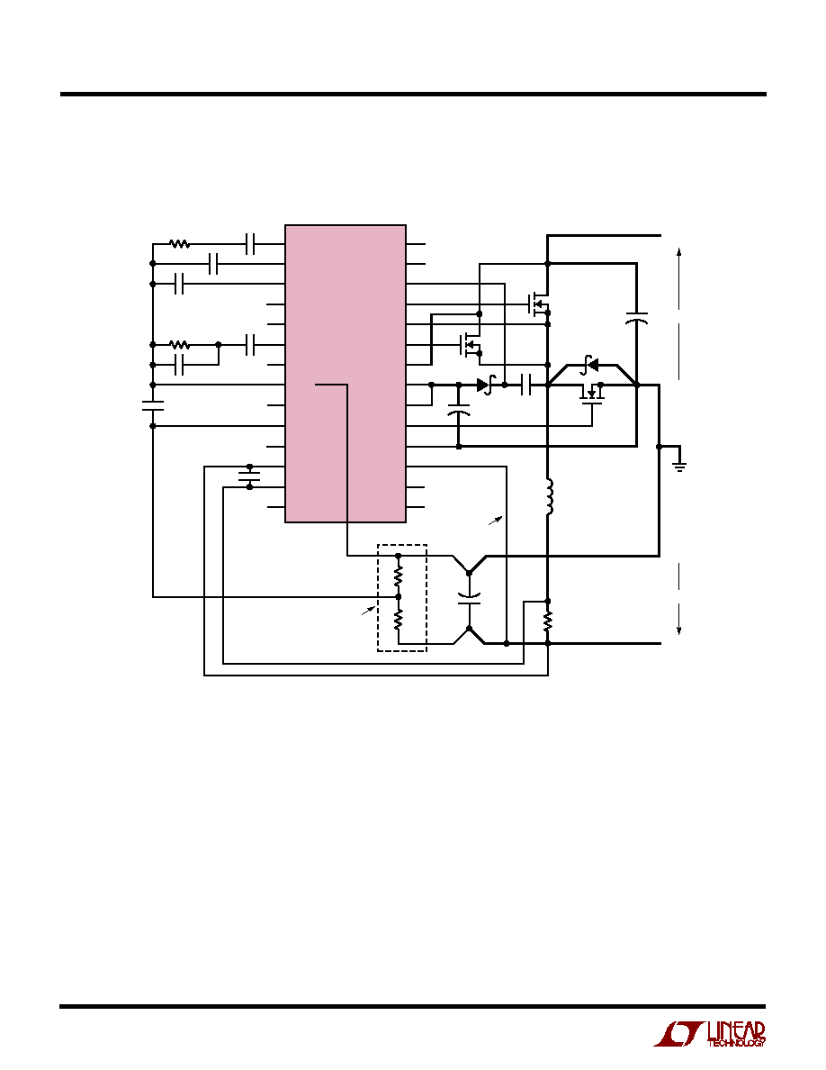
24
LTC1436A
LTC1436-PLL-A/LTC1437A
+
+
+
1
2
3
4
5
6
7
8
9
10
11
12
13
14
28
27
26
25
24
23
22
21
20
19
18
17
16
15
PLL LPF
C
OSC
RUN/SS
LBO
LBI
I
TH
SFB
SGND
V
PROG
V
OSENSE
NC
SENSE
≠
SENSE
+
AUXON
PLLIN
POR
BOOST
TGL
SW
TGS
V
IN
INTV
CC
DRV
CC
BG
PGND
EXTV
CC
AUXDR
AUXFB
R
LP
R
C
C
LP
C
C
1000pF
OPEN
100pF
R1
C
OUT
R
SENSE
L1
4.7
µ
F
C
B
0.1
µ
F
D
B
M3
D1
EXT CLOCK
LTC1437A
+
≠
+
≠
M1
M2
1437 F15
C
IN
R2
OUTPUT DIVIDER
REQUIRED WITH
V
PRGM
OPEN
BOLD LINES INDICATE HIGH CURRENT PATHS
5V EXT V
CC
CONNECTION
AUX
ON/OFF
C
SS
C
C2
C
OSC
V
IN
V
OUT
Figure 15. LTC1437A Layout Diagram
APPLICATIO
N
S I
N
FOR
M
ATIO
N
W
U
U
U
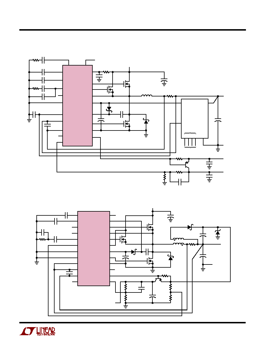
25
LTC1436A
LTC1436A-PLL/LTC1437A
TYPICAL APPLICATIO
N
S
U
Intel Mobile CPU VID Core Power Converter with 1.8V I/O Supply
1
2
3
4
5
6
7
8
9
10
11
12
24
23
22
21
20
19
18
17
16
15
14
13
+
+
+
+
+
C
OSC
RUN/SS
LBO
LBI
I
TH
SFB
SGND
V
PROG
V
OSENSE
SENSE
≠
SENSE
+
AUXON
POR
BOOST
TGL
SW
TGS
V
IN
INTV
CC
BG
PGND
EXTV
CC
AUXDR
AUXFB
C
OSC
68pF
C
IN
22
µ
F
35V
◊
2
C
SEC
3.3
µ
F
35V
C
OUT
100
µ
F
10V
◊
2
C
C
510pF
M1
S4412DY
M2
Si4412DY
MBRS140T3
SGND
(PIN 7)
1436 TA02
T1
10
µ
H
1:1
47k
R
SENSE
0.025
MBRS1100T3
V
IN
4.5V TO 28V
2N2905A
V
OUT2
5V
100mA
V
OUT
3.3V
4A
M3
IRLML2803
4.7
µ
F
3.3
µ
F
R8
180k
R7
56k
R6
430k
R5
100k
51pF
0.1
µ
F
CMDSH-3
LTC1436A
1000pF
AUX
ON/OFF
R
C
10k
C
C2
51pF
C
SS
0.1
µ
F
24V
LTC1436A 3.3V/4A Fixed Output with 5V Auxiliary Output
1436 TA09
+
+
C
C
220pF
100pF
R
C
10k
C
SS
0.1
µ
F
C
OSC
43pF
1000pF
AUX
ON/OFF
L1
3.3
µ
H
R
SENSE
0.015
V
IN
4.5V TO 22V
V
CORE
1.3V TO 2V
7A
V
IN2
3.3V
SGND
(PIN 6)
0.22
µ
F
0.1
µ
F
10k
C
IN
22
µ
F
35V
X2
4.7
µ
F
M1
Si4410DY
M2
Si4410DY
*D
B
D1
MBRS140T3
C
C2
1000pF
4.7
+
C
OUT
820
µ
F
4V
◊
2
V
CC
FB
0
1 2
VID
LTC1706-19
FROM
µ
P
3
7
3
6
5
8 1 2
4
GND
SENSE
V
IN
2
3
4
7
6
8
INTV
CC
C
OSC
EXTERNAL
FREQUENCY
SYNCHRONIZATION
SGND
V
PROG
PLL LPF
PLLIN
V
OSENSE
TGL
TGS
SW
AUXDR
PGND
BG
BOOST
RUN/SS
I
TH
SENSE
+
AUXON
AUXFB
SENSE
≠
LTC1436A-PLL
V
I/O
1.8V
150mA
M3
IRLML2803
18
1
24
0.1
µ
F
21
19
20
17
22
16
15
13
9
10
11
12
47k
10.5k
20k
51pF
MMBT2907L
47
µ
F
4V**
*CMDSH-3
**INPUT CAPACITOR MAY NOT BE NECESSARY IF
3.3V SUPPLY HAS SUFFICIENT CAPACITANCE
47
µ
F
4V
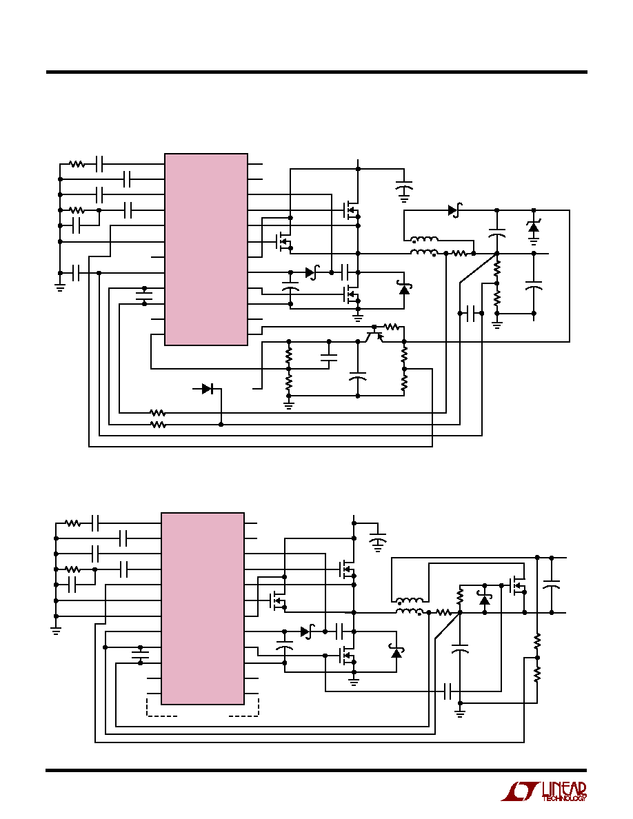
26
LTC1436A
LTC1436-PLL-A/LTC1437A
TYPICAL APPLICATIO
N
S
U
LTC1436A-PLL 2.5V/5V Adjustable Output with
Foldback Current limiting and 5V Auxiliary Output
1
2
3
4
5
6
7
8
9
10
11
12
24
23
22
21
20
19
18
17
16
15
14
13
+
+
PLL LPF
C
OSC
RUN/SS
I
TH
SFB
SGND
V
PROG
V
OSENSE
SENSE
≠
SENSE
+
AUXON
AUXFB
PLLIN
POR
BOOST
TGL
SW
TGS
V
IN
INTV
CC
BG
PGND
EXTV
CC
AUXDR
C
LP
0.01
µ
F
C
IN
22
µ
F/35V
◊
2
EXT
CLOCK
+
C
OUT1
100
µ
F
10V
◊
2
C
C
510pF
M1
Si4412DY
M2
Si4412DY
MBRS140T3
SGND
(PIN 6)
1436 TA04
T1
10
µ
H
1:2.2
47k
R
SENSE
0.025
V
IN
4.5V TO 28V
V
OUT2
12V
0.5A
V
OUT1
3.3V
4A
M3
IRLML2803
M4, IRLL014
4.7
µ
F
0.01
µ
F
11.3k
1%k
100k
1%k
0.1
µ
F
CMDSH-3
CMDSH-3
LTC1436A-PLL
1000pF
COMP
ON/OFF
R
C,
10k
R
LP
10k
C
C2
51pF
C
SS
0.1
µ
F
C
OSC
68pF
COMPARATOR
+
C
SEC
3.3
µ
F
35V
T1: DALE LPE6562-A092
LTC1436A-PLL 5V/3A Fixed Output with 12V/200mA Auxiliary Output
and Uncommitted Comparator
1
2
3
4
5
6
7
8
9
10
11
12
24
23
22
21
20
19
18
17
16
15
14
13
+
+
+
+
+
PLL LPF
C
OSC
RUN/SS
I
TH
SFB
SGND
V
PROG
V
OSENSE
SENSE
≠
SENSE
+
AUXON
AUXFB
PLLIN
POR
BOOST
TGL
SW
TGS
V
IN
INTV
CC
BG
PGND
EXTV
CC
AUXDR
C
LP
0.01
µ
F
C
IN
22
µ
F
35V
◊
2
EXT
CLOCK
C
SEC
3.3
µ
F
35V
C
OUT
100
µ
F
10V
◊
2
R1
100k
1%
R2
35.7k
1%
C
C
510pF
OPEN
M1
Si4410DY
M2
Si4410DY
MBRS140T3
SGND
(PIN 6)
1436 TA03
T1
10
µ
H
1:1.6
47k
R
SENSE
0.02
MBRS1100T3
V
IN
4.5V TO 24V
ZETEX
FZT749
V
OUT2
5V
0.2A
I
TH
(PIN 4)
1N4148
V
OUT
2.5V
5A
24V
M3
IRLML2803
4.7
µ
F
3.3
µ
F
R8
180k
R7
56k
R6
430k
R5
100k
51pF
0.1
µ
F
CMDSH-3
LTC1436A-PLL
100
100
1000pF
AUX
ON/OFF
R
C,
10k
R
LP
10k
C
C2
51pF
C
SS
0.1
µ
F
C
OSC
68pF
100pF
100pF
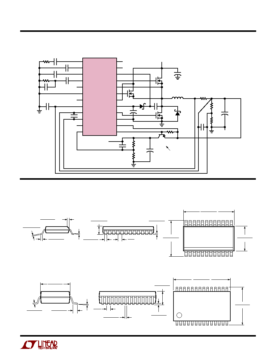
27
LTC1436A
LTC1436A-PLL/LTC1437A
G28 SSOP 0694
0.301 ≠ 0.311
(7.65 ≠ 7.90)
1
2 3
4
5
6 7 8
9 10 11 12
14
13
0.397 ≠ 0.407*
(10.07 ≠ 10.33)
25
26
22 21 20 19 18 17 16 15
23
24
27
28
0.068 ≠ 0.078
(1.73 ≠ 1.99)
0.002 ≠ 0.008
(0.05 ≠ 0.21)
0.0256
(0.65)
BSC
0.010 ≠ 0.015
(0.25 ≠ 0.38)
0.005 ≠ 0.009
(0.13 ≠ 0.22)
0
∞
≠ 8
∞
0.022 ≠ 0.037
(0.55 ≠ 0.95)
0.205 ≠ 0.212**
(5.20 ≠ 5.38)
DIMENSIONS DO NOT INCLUDE MOLD FLASH. MOLD FLASH
SHALL NOT EXCEED 0.006" (0.152mm) PER SIDE
DIMENSIONS DO NOT INCLUDE INTERLEAD FLASH. INTERLEAD
FLASH SHALL NOT EXCEED 0.010" (0.254mm) PER SIDE
*
**
Information furnished by Linear Technology Corporation is believed to be accurate and reliable.
However, no responsibility is assumed for its use. Linear Technology Corporation makes no represen-
tation that the interconnection of its circuits as described herein will not infringe on existing patent rights.
GN24 (SSOP) 0595
* DIMENSION DOES NOT INCLUDE MOLD FLASH. MOLD FLASH
SHALL NOT EXCEED 0.006" (0.152mm) PER SIDE
** DIMENSION DOES NOT INCLUDE INTERLEAD FLASH. INTERLEAD
FLASH SHALL NOT EXCEED 0.010" (0.254mm) PER SIDE
0.016 ≠ 0.050
(0.406 ≠ 1.270)
0.015
±
0.004
(0.38
±
0.10)
◊
45
∞
0
∞
≠ 8
∞
TYP
0.0075 ≠ 0.0098
(0.191 ≠ 0.249)
0.053 ≠ 0.069
(1.351 ≠ 1.748)
0.008 ≠ 0.012
(0.203 ≠ 0.305)
0.004 ≠ 0.009
(0.102 ≠ 0.249)
0.025
(0.635)
BSC
0.337 ≠ 0.344*
(8.560 ≠ 8.737)
1
2
3
4
5
6
7
8
9 10 11 12
0.229 ≠ 0.244
(5.817 ≠ 6.198)
0.150 ≠ 0.157**
(3.810 ≠ 3.988)
16
17
18
19
20
21
22
23
24
15 14 13
GN Package
24-Lead Plastic SSOP (Narrow 0.150)
(LTC DWG # 05-08-1641)
Dimensions in inches (millimeters) unless otherwise noted.
PACKAGE DESCRIPTIO
N
U
TYPICAL APPLICATIO
N
S
U
LTC1436A-PLL Low Noise High Efficiency 5V/1A Regulaor
1
2
3
4
5
6
7
8
9
10
11
12
24
23
22
21
20
19
18
17
16
15
14
13
+
+
+
+
PLL LPF
C
OSC
RUN/SS
I
TH
SFB
SGND
V
PROG
V
OSENSE
SENSE
≠
SENSE
+
AUXON
AUXFB
PLLIN
POR
BOOST
TGL
SW
TGS
V
IN
INV
CC
BG
PGND
EXTV
CC
AUXDR
C
LP
0.01
µ
F
C
IN
22
µ
F
35V
EXT CLOCK
250kHz
SFB = 0V: CONTINUOUS MODE
SFB = 5V: BURST ENABLED
C
OUT
100
µ
F
10V
R1
240k
1%
R2
56k
1%
100pF
100pF
C
C
510pF
M1
IRF7201
M2
IRF7201
MBRS140T3
SGND
(PIN 6)
1436 TA07
L1
50
µ
H
47k
R
SENSE
0.1
V
IN
5.5V TO 28V
ZETEX
FMMT549
HEAT SINK
V
OUT
5V
1A
V1
6.3V
M3
IRLML2803
4.7
µ
F
22
µ
F
R8
180k
1%
R7
56k
1%
51pF
0.1
µ
F
CMDSH-3
LTC1436A-PLL
1000pF
V
OUT
ON/OFF
R
C,
10k
R
LP
10k
C
C2
51pF
C
SS
0.1
µ
F
C
OSC
39pF
G Package
28-Lead Plastic SSOP (0.209)
(LTC DWG # 05-08-1640)
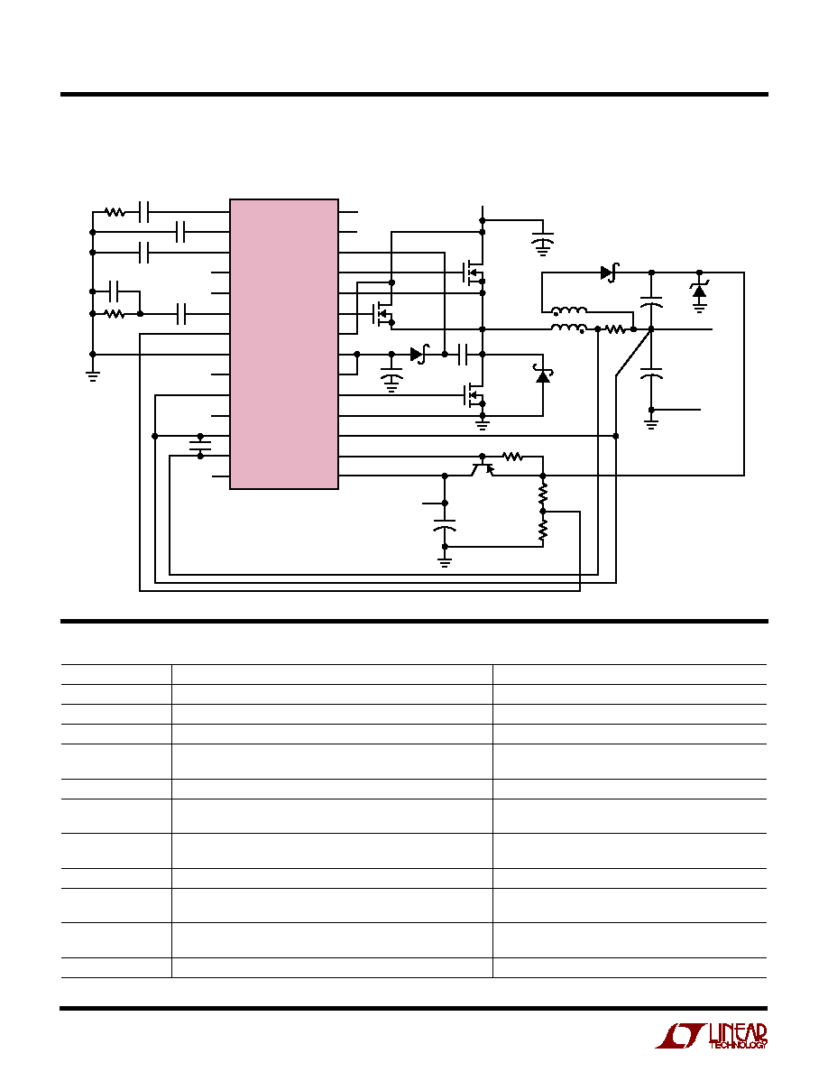
28
LTC1436A
LTC1436-PLL-A/LTC1437A
14367afa LT/TP 0898 REV A 2K ∑ PRINTED IN USA
©
LINEAR TECHNOLOGY CORPORATION 1996
TYPICAL APPLICATIO
N
U
LTC1437A 5V/3A Fixed Output with 12V Auxiliary Output
1
2
3
4
5
6
7
8
9
10
11
12
13
14
28
27
26
25
24
23
22
21
20
19
18
17
16
15
+
+
+
+
PLL LPF
C
OSC
RUN/SS
LBO
LBI
I
TH
SFB
SGND
V
PROG
V
OSENSE
NC
SENSE
≠
SENSE
+
AUXON
PLLIN
POR
BOOST
TGL
SW
TGS
V
IN
INV
CC
DRV
CC
BG
PGND
EXTV
CC
AUXDR
AUXFB
C
LP
0.01
µ
F
C
IN
22
µ
F
35V
◊
2
EXT
CLOCK
C
SEC
3.3
µ
F
35V
C
OUT
100
µ
F
10V
◊
2
C
C
510pF
INT V
CC
M1
IRF7403
M2
IRF7403
MBRS140T3
SGND
(PIN 8)
1436 TA06
T1
22
µ
H
1:2.2
47k
R
SENSE
0.03
MBRS1100T3
V
IN
5.5V TO 28V
MMBT2907
V
OUT2
12V
0.2A
V
OUT
5V
3A
24V
M3
IRLML2803
4.7
µ
F
3.3
µ
F
R6
1M
T1: DALE LPE6562-A092
R5
100k
0.1
µ
F
CMDSH-3
LTC1437A
1000pF
AUX
ON/OFF
R
C
10k
R
LP
10k
C
C2
51pF
C
SS
0.1
µ
F
C
OSC
39pF
+
RELATED PARTS
PART NUMBER
DESCRIPTION
COMMENTS
LTC1142HV/LTC1142
Dual High Efficiency Synchronous Step-Down Switching Regulators
Dual Synchronous, V
IN
20V
LTC1148HV/LTC1148
High Efficiency Step-Down Switching Regulator Controllers
Synchronous, V
IN
20V
LTC1159
High Efficiency Synchronous Step-Down Switching Regulator
Synchronous, V
IN
40V, For Logic Threshold FETs
LT
Æ
1375/LT1376
1.5A, 500kHz Step-Down Switching Regulators
High Frequency, Small Inductor, High Efficiency
Switchers, 1.5A Switch
LTC1430
High Power Step-Down Switching Regulator Controller
High Efficiency 5V to 3.3V Conversion at Up to 15A
LTC1435A
High Efficency, Low Noise Synchronous Step-Down
16-Pin Narrow SO and SSOP
Switching Regulator
LTC1438/LTC1439
Dual High Efficiency, Low Noise, Synchronous Step-Down
Full-Featured Dual Controllers
Switching Regulators
LT1510
Constant-Voltage/ Constant-Current Battery Charger
1.3A, Li-Ion, NiCd, NiMH, Pb-Acid Charger
LTC1538-AUX
Dual High Efficiency, Low Noise, Synchronous Step-Down
5V Standby in Shutdown
Switching Regulator
LTC1539
Dual High Efficiency, Low Noise, Synchronous Step-Down
5V Standby in Shutdown
Switching Regulator
LTC1706-19
VID Voltage Programmer
Intel Mobile Pentium
Æ
II Compliant
Pentium is a registered trademark of Intel Corp.
Linear Technology Corporation
1630 McCarthy Blvd., Milpitas, CA 95035-7417
(408) 432-1900
q
FAX: (408) 434-0507
q
www.linear-tech.com