Äîêóìåíòàöèÿ è îïèñàíèÿ www.docs.chipfind.ru
1
LTC1438/LTC1439
Dual High Efficiency,
Low Noise, Synchronous
Step-Down Switching Regulators
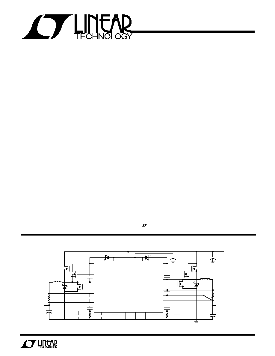
Figure 1. High Efficiency Dual 5V/3V Step-Down Converter
s
Maintains Constant Frequency at Low Output Currents
s
Dual N-Channel MOSFET Synchronous Drive
s
Programmable Fixed Frequency (PLL Lockable)
s
Wide V
IN
Range: 3.5V to 36V Operation
s
Ultrahigh Efficiency
s
Very Low Dropout Operation: 99% Duty Cycle
s
Low Dropout, 0.5A Linear Regulator for VPP
Generation or Low Noise Audio Supply
s
Built-In Power-On Reset Timer
s
Programmable Soft Start
s
Low-Battery Detector
s
Remote Output Voltage Sense
s
Foldback Current Limiting (Optional)
s
Pin Selectable Output Voltage
s
Logic-Controlled Micropower Shutdown: I
Q
< 30
µ
A
s
Output Voltages from 1.19V to 9V
s
Available in 28- and 36-Lead SSOP Packages
The LTC
®
1438/LTC1439 are dual, synchronous step-
down switching regulator controllers which drive external
N-channel power MOSFETs in a phase-lockable fixed
frequency architecture. The Adaptive Power
TM
output stage
selectively drives two N-channel MOSFETs at frequencies
up to 400kHz while reducing switching losses to maintain
high efficiencies at low output currents.
An auxiliary 0.5A linear regulator using an external PNP
pass device provides a low noise, low dropout voltage
source. A secondary winding feedback control pin (SFB1)
guarantees regulation regardless of load on the main
output by forcing continuous operation.
An additional comparator is available for use as a low
battery detector. A power-on reset timer (POR) is included
which generates a signal delayed by 65536/f
CLK
(typ
300ms) after the output is within 5% of the regulated
output voltage. Internal resistive dividers provide pin
selectable output voltages with remote sense capability on
one of the two outputs.
The operating current levels are user-programmable via
external current sense resistors. Wide input supply range
allows operation from 3.5V to 30V (36V maximum).
FEATURES
DESCRIPTIO
N
U
, LTC and LT are registered trademarks of Linear Technology Corporation.
Adaptive Power is a trademark of Linear Technology Corporation.
TYPICAL APPLICATIO
N
U
BOOST 2
BOOST 1
TGL2
TGS2
SW2
BG2
SENSE
+
2
SENSE
2
V
OSENSE2
I
TH2
TGL1
M3*
M1
M2
TGS1
D1
MBR140T3
V
OUT1
5V
3.5A
V
OUT2
3.3V
3.5A
L1
10
µ
H
SW1
BG1
LTC1439
SENSE
+
1
SENSE
1
C
SS1
0.1
µ
F
C
C1
1000pF
C
OUT1
220
µ
F
10V
R
SENSE1
0.03
R
SENSE2
0.03
C
OUT
220
µ
F
10V
R
C1
10k
I
TH1
RUN/SS2
PGND
SGND
V
PROG2
C
DSC
INTV
CC
D
B2
, CMDSH-3
D
B1
, CMDSH-3
V
IN
V
PROG1
RUN/SS1
D2
MBR140T3
C
B1
0.1
µ
F
C
B2
,
0.1
µ
F
4.7
µ
F
16V
M6*
1438 F01
M4
1000pF
1000pF
C
OSC
56pF
C
SS2
0.1
µ
F
C
C1A
220pF
M1, M2, M4, M5: Si4412DY
M3, M6: IRLML2803
*NOT REQUIRED FOR LTC1438
C
C2A
470pF
C
C2
1000pF
R
C2
10k
+
L2
10
µ
H
V
IN
5.2V TO 28V
+
+
C
IN
22
µ
F
35V
×
4
+
BOLD LINES INDICATE HIGH CURRENT PATHS
M5
s
Notebook and Palmtop Computers, PDAs
s
Portable Instruments
s
Battery-Operated Devices
s
DC Power Distribution Systems
APPLICATIO
N
S
U
2
LTC1438/LTC1439
ABSOLUTE
M
AXI
M
U
M
RATINGS
W
W
W
U
Input Supply Voltage (V
IN
)....................... 36V to 0.3V
Topside Driver Voltage (BOOST 1, 2) ...... 42V to 0.3V
Switch Voltage (SW1, 2) ...................... V
IN
+ 5V to 5V
EXTV
CC
Voltage....................................... 10V to 0.3V
POR2, LBO Voltages ............................... 12V to 0.3V
AUXFB Voltage ....................................... 20V to 0.3V
AUXDR Voltage ....................................... 28V to 0.3V
SENSE
+
1, SENSE
+
2, SENSE
1, SENSE
2,
V
OSENSE2
Voltages ................... INTV
CC
+ 0.3V to 0.3V
V
PROG1
, V
PROG2
Voltages ................... INTV
CC
to 0.3V
PLL LPF, I
TH1
, I
TH2
Voltages .................. 2.7V to 0.3V
AUXON, PLLIN, SFB1,
RUN/SS1, RUN/SS2, LBI Voltages ......... 10V to 0.3V
Peak Output Current < 10
µ
s (TGL1, 2, BG1, 2) ......... 2A
Peak Output Current < 10
µ
s (TGS1, 2) .............. 250mA
INTV
CC
Output Current ....................................... 50mA
Operating Ambient Temperature Range
Commercial ........................................... 0
°
C to 70
°
C
Industrial .......................................... 40
°
C to 85
°
C
Junction Temperature (Note 1) ............................ 125
°
C
Storage Temperature Range ................ 65
°
C to 150
°
C
Lead Temperature (Soldering, 10 sec) ................. 300
°
C
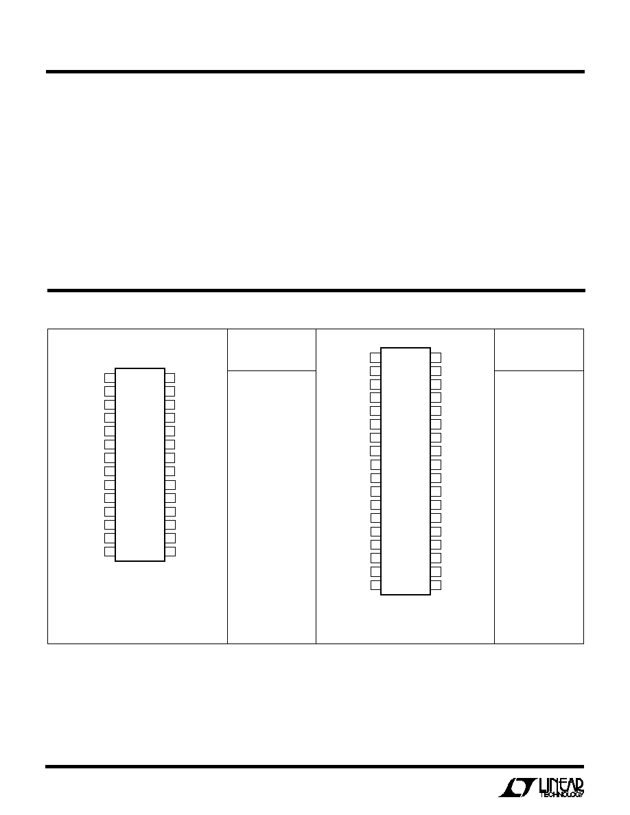
ORDER
PART NUMBER
LTC1439CG
LTC1439IG
LTC1439CGW
LTC1439IGW
ORDER
PART NUMBER
Consult factory for Military grade parts.
PACKAGE/ORDER I
N
FOR
M
ATIO
N
W
U
U
LTC1438CG
LTC1438CG-ADJ
LTC1438IG
LTC1438IG-ADJ
LTC1438XCG
T
JMAX
= 125
°
C,
JA
= 95
°
C/ W
1
2
3
4
5
6
7
8
9
10
11
12
13
14
TOP VIEW
G PACKAGE
28-LEAD PLASTIC SSOP
28
27
26
25
24
23
22
21
20
19
18
17
16
15
SENSE
+
1
SENSE
1
V
PROG1
*
I
TH1
POR2**
C
OSC
SGND
LBI
LBO
SFB1
I
TH2
V
OSENSE2
SENSE
2
SENSE
+
2
RUN/SS1
BOOST 1
TGL1
SW1
V
IN
BG1
INTV
CC
PGND
BG2
EXTV
CC
SW2
TGL2
BOOST 2
RUN/SS2
V
OSENSE1
ON LTC1438-ADJ
NC ON THE LTC1438XCG
*
**
1
2
3
4
5
6
7
8
9
10
11
12
13
14
15
16
17
18
TOP VIEW
GW PACKAGE
36-LEAD PLASTIC SSOP
G PACKAGE
36-LEAD PLASTIC SSOP
36
35
34
33
32
31
30
29
28
27
26
25
24
23
22
21
20
19
RUN/SS1
SENSE
+
1
SENSE
1
V
PROG1
I
TH1
POR2
C
OSC
SGND
LBI
LBO
SFB1
I
TH2
V
PROG2
V
OSENSE2
SENSE
2
SENSE
+
2
RUN/SS2
AUXDR
PLL LPF
PLLIN
BOOST 1
TGL1
SW1
TGS1
V
IN
BG1
INTV
CC
PGND
BG2
EXTV
CC
TGS2
SW2
TGL2
BOOST 2
AUXON
AUXFB
T
JMAX
= 125
°
C,
JA
= 95
°
C/ W (G)
T
JMAX
= 125
°
C,
JA
= 85
°
C/ W (GW)
3
LTC1438/LTC1439
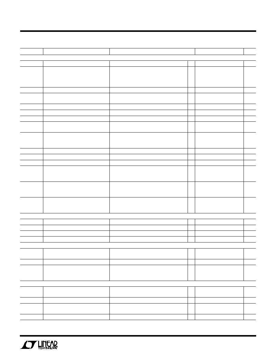
ELECTRICAL CHARACTERISTICS
T
A
= 25
°
C, V
IN
= 15V, V
RUN/SS1,2
= 5V unless otherwise noted.
SYMBOL
PARAMETER
CONDITIONS
MIN
TYP
MAX
UNITS
Main Control Loops
I
IN
V
OSENSE1,2
Feedback Current
V
PROG1,
V
PROG2
Pins Open (Note 2)
10
50
nA
V
OUT1,2
Regulated Output Voltage
(Note 2)
1.19V (Adjustable) Selected
V
PROG1,
V
PROG2
Pins Open
q
1.178
1.19
1.202
V
3.3V Selected
V
PROG1,
V
PROG2
= 0V
q
3.220
3.30
3.380
V
5V Selected
V
PROG1,
V
PROG2
= INT V
CC
q
4.900
5.00
5.100
V
V
LINEREG1,2
Reference Voltage Line Regulation
V
IN
= 3.6V to 20V (Note 2), V
PROG1,2
Pins Open
0.002
0.01
%/V
V
LOADREG1,2
Output Voltage Load Regulation
I
TH1,2
Sinking 5
µ
A (Note 2)
q
0.5
0.8
%
I
TH1,2
Sourcing 5
µ
A
q
0.5
0.8
%
V
SFB1
Secondary Feedback Threshold
V
SFB1
Ramping Negative
q
1.16
1.19
1.22
V
I
SFB1
Secondary Feedback Current
V
SFB1
= 1.5V
1
2
µ
A
V
OVL
Output Overvoltage Lockout
V
PROG1,2
, SENSE
1 and V
OSENSE1,2
Pins Open
1.24
1.28
1.32
V
I
PROG1,2
V
PROG1,2
Input Current
0.5V > V
PROG1,2
3
6
µ
A
INTV
CC
0.5V < V
PROG1,2
< INTV
CC
3
6
µ
A
I
Q
Input DC Supply Current
EXTV
CC
= 5V (Note 3)
Normal Mode
3.6V < V
IN
< 30V, V
AUXON
= 0V
320
µ
A
Shutdown
V
RUN/SS1,2
= 0V, 3.6V < V
IN
< 15V
16
30
µ
A
V
RUN/SS1,2
Run Pin Threshold
q
0.8
1.3
2
V
I
RUN/SS1,2
Soft Start Current Source
V
RUN/SS1,2
= 0V
1.5
3
4.5
µ
A
V
SENSE(MAX)
Maximum Current Sense Threshold
V
OSENSE1,2
= 0V, 5V V
PROG1,2
= Pins Open
130
150
180
mV
TGL1, 2 t
r
, t
f
TGL1, TGL2 Transition Time
Rise Time
C
LOAD
= 3000pF
50
150
ns
Fall Time
C
LOAD
= 3000pF
50
150
ns
TGS1, 2 t
r
, t
f
TGS1, TGS2 Transition Time
Rise Time
C
LOAD
= 500pF
100
150
ns
Fall Time
C
LOAD
= 500pF
50
150
ns
BG1, 2 t
r
, t
f
BG1, BG2 Transition Time
Rise Time
C
LOAD
= 3000pF
50
150
ns
Fall Time
C
LOAD
= 3000pF
50
150
ns
Internal V
CC
Regulator
V
INTVCC
Internal V
CC
Voltage
6V < V
IN
< 30V, V
EXTVCC
= 4V
q
4.8
5.0
5.2
V
V
LDO
INT
INTV
CC
Load Regulation
I
INTVCC
= 20mA, V
EXTVCC
= 4V
0.2
1
%
V
LDO
EXT
EXTV
CC
Voltage Drop
I
INTVCC
= 20mA, V
EXTVCC
= 5V
170
300
mV
V
EXTVCC
EXTV
CC
Switchover Voltage
I
INTVCC
= 20mA, EXTV
CC
Ramping Positive
q
4.5
4.7
V
Oscillator and Phase-Locked Loop
f
OSC
Oscillator Frequency
C
OSC
= 100pF, LTC1439: PLL LPF = 0V (Note 4)
112
125
138
kHz
VCO High
LTC1439, V
PLLLPF
= 2.4V
200
240
kHz
R
PLLIN
PLLIN
Input Resistance
50
k
I
PLLLPF
Phase Detector Output Current
LTC1439
Sinking Capability
f
PLLIN
< f
OSC
10
15
20
µ
A
Sourcing Capability
f
PLLIN
> f
OSC
10
15
20
µ
A
Power-On Reset
V
SATPOR2
POR2 Saturation Voltage
I
POR2
= 1.6mA, V
OSENSE2
= 1V,
0.6
1
V
V
PROG2
Pin Open
I
LPOR2
POR2 Leakage
V
POR2
= 12V, V
OSENSE2
= 1.2V, V
PROG2
Pin Open
0.2
1
µ
A
V
THPOR2
POR2 Trip Voltage
V
PROG2
Pin Open % of V
REF
V
OSENSE2
Ramping Negative
11
7.5
4
%
t
DPOR2
POR2 Delay
V
PROG2
Pin Open
65536
Cycles
4
LTC1438/LTC1439
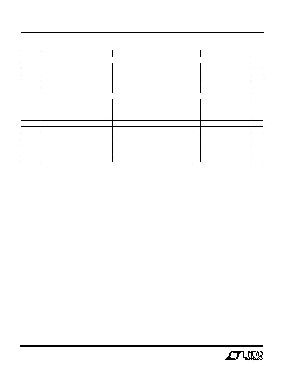
ELECTRICAL CHARACTERISTICS
T
A
= 25
°
C, V
IN
= 15V, V
RUN/SS1,2
= 5V unless otherwise noted.
The
q
denotes specifications which apply over the full operating
temperature range.
Note 1: T
J
is calculated from the ambient temperature T
A
and power
dissipation P
D
according to the following formulas:
LTC1438CG, LTC1439CG: T
J
= T
A
+ (P
D
)(95
°
C/W)
LTC1439CGW: T
J
= T
A
+ (P
D
)(85
°
C/W)
Note 2: The LTC1438 and LTC1439 are tested in a feedback loop which
servos V
OSENSE1,2
to the balance point for the error amplifier
(V
ITH1,2
= 1.19V).
Note 3: Dynamic supply current is higher due to the gate charge being
delivered at the switching frequency. See Applications Information.
Note 4: Oscillator frequency is tested by measuring the C
OSC
charge and
discharge current (I
OSC
) and applying the formula:
f
OSC
(kHz) = 8.4(10
8
)[C
OSC
(pF) + 11]
1
(1/I
CHG
+ 1/I
DISC
)
1
Note 5: The auxiliary regulator is tested in a feedback loop which servos
V
AUXFB
to the balance point for the error amplifier. For applications with
V
AUXDR
> 9.5V, V
AUXFB
uses an internal resistive divider. See Applications
Information section.
SYMBOL
PARAMETER
CONDITIONS
MIN
TYP
MAX
UNITS
Low-Battery Comparator
V
SATLBO
LBO Saturation Voltage
I
LBO
= 1.6mA, V
LBI
= 1.1V
0.6
1
V
I
LLBO
LBO Leakage
V
LBO
= 12V, V
LBI
= 1.4V
q
0.01
1
µ
A
V
THLB1
LBI Trip Voltage
High to Low Transition on LBO
q
1.16
1.19
1.22
V
I
INLB1
LBI Input Current
V
LBI
= 1.19V
q
1
50
nA
V
HYSLBO
LBO Hysteresis
20
mV
Auxiliary Regulator/Comparator
I
AUXDR
AUXDR Current
V
EXTVCC
= 0V
Max Current Sinking Capability
V
AUXDR
= 4V, V
AUXFB
= 1.0V, V
AUXON
= 5V
10
15
mA
Control Current
V
AUXDR
= 5V, V
AUXFB
= 1.5V, V
AUXON
= 5V
1
5
µ
A
Leakage when OFF
V
AUXDR
= 24V, V
AUXFB
= 1.5V, V
AUXON
= 0V
0.01
1
µ
A
I
INAUXFB
AUXFB Input Current
V
AUXFB
= 1.19V, V
AUXON
= 5V
0.01
1
µ
A
I
INAUXON
AUXON Input Current
V
AUXON
= 5V
0.01
1
µ
A
V
THAUXON
AUXON Trip Voltage
V
AUXDR
= 4V, V
AUXFB
= 1V
1.0
1.19
1.4
V
V
SATAUXDR
AUXDR Saturation Voltage
I
AUXDR
= 1.6mA, V
AUXFB
= 1V, V
AUXON
= 5V
0.4
0.8
V
V
AUXFB
AUXFB Voltage
V
AUXON
= 5V, 11V < V
AUXDR
< 24V (Note 5)
q
11.5
12.0
12.5
V
V
AUXON
= 5V, 3V < V
AUXDR
< 7V
q
1.14
1.19
1.24
V
V
THAUXDR
AUXFB Divider Disconnect Voltage
V
AUXON
= 5V (Note 5); Ramping Negative
7.5
8.5
9.5
V
5
LTC1438/LTC1439
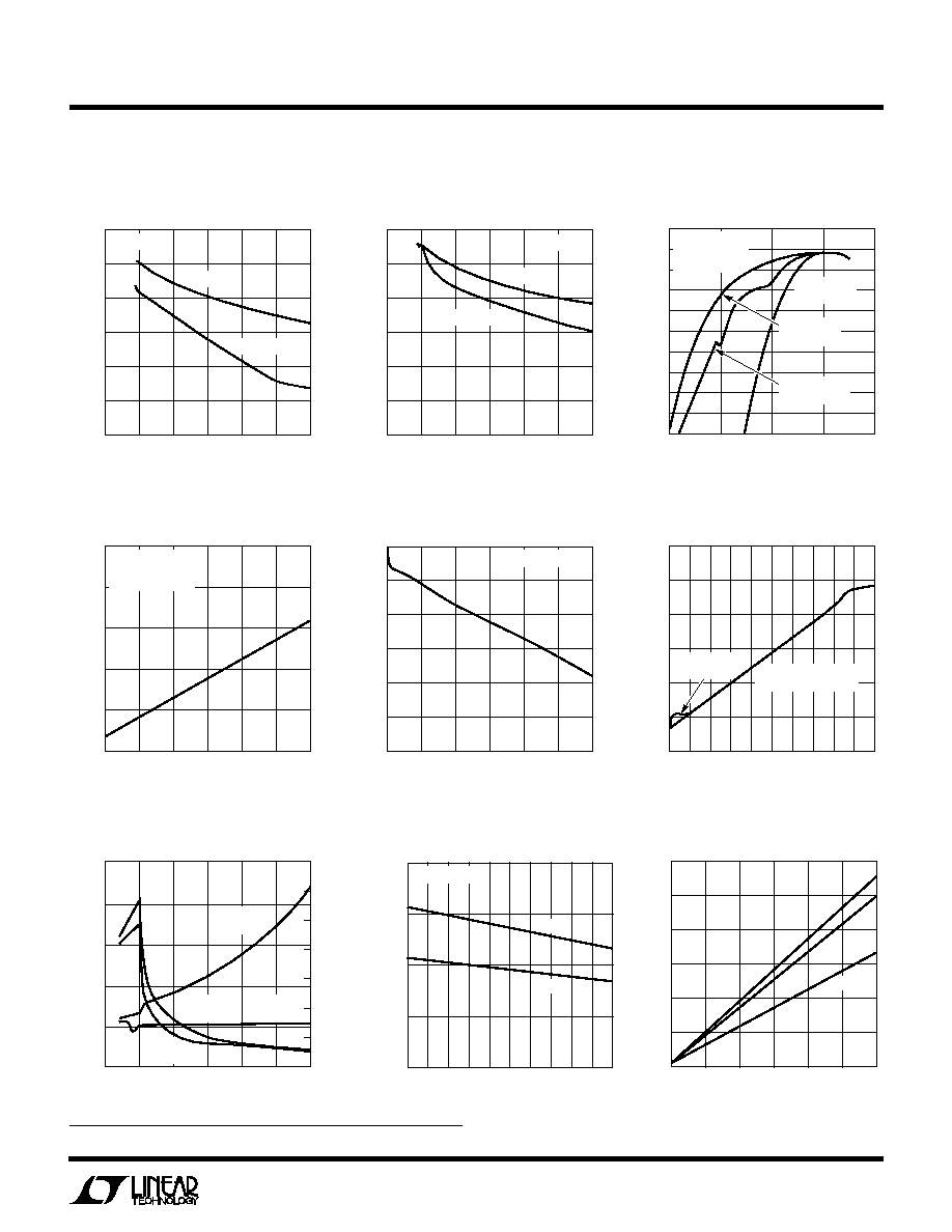
TYPICAL PERFOR
M
A
N
CE CHARACTERISTICS
U
W
Efficiency vs Input Voltage
V
OUT
= 3.3V
V
IN
V
OUT
Dropout Voltage
vs Load Current
Efficiency vs Load Current
V
ITH
Pin Voltage vs Output Current
Load Regulation
Input Supply Current
vs Input Voltage
EXTV
CC
Switch Drop
vs INTV
CC
Load Current
INPUT VOLTAGE (V)
0
70
EFFICIENCY (%)
75
80
85
90
100
5
10
15
20
1438 G01
25
30
95
I
LOAD
= 1A
I
LOAD
= 100mA
V
OUT
= 3.3V
Efficiency vs Input Voltage
V
OUT
= 5V
INPUT VOLTAGE (V)
0
70
EFFICIENCY (%)
75
80
85
90
100
5
10
15
20
1438 G02
25
30
95
I
LOAD
= 1A
I
LOAD
= 100mA
V
OUT
= 5V
LOAD CURRENT (A)
0.001
50
EFFICIENCY (%)
55
65
70
75
100
85
0.01
0.1
1
1435 G03
60
90
95
80
10
Adaptive Power
MODE
CONTINUOUS
MODE
V
IN
= 10V
V
OUT
= 5V
R
SENSE
= 0.33
Burst Mode
®
OPERATION
LOAD CURRENT (A)
0
0
V
IN
V
OUT
(V)
0.2
0.1
0.3
0.4
0.5
0.5
1.0
1.5
2.0
1438 G04
2.5
3.0
R
SENSE
= 0.033
V
OUT
DROP OF 5%
M1, M2: Si4412
LOAD CURRENT (A)
0
V
OUT
(%)
0
0.5
1.0
1.5
2.0
1438 G05
2.5
3.0
0.25
0.50
0.75
1.00
1.25
1.50
R
SENSE
= 0.033
OUTPUT CURRENT (%)
0
V
ITH
(V)
1.0
2.0
3.0
0.5
1.5
2.5
20
40
60
80
1438 G06
100
10
0
30
50
70
90
Burst Mode
OPERATION
CONTINUOUS/Adaptive
Power MODE
INPUT VOLTAGE (V)
0
0
SUPPLY CURRENT (mA)
SHUTDOWN CURRENT (
µ
A)
0.5
1.0
1.5
2.0
2.5
0
5
10
15
20
25
30
35
5
10
15
20
1438 G07
25
30
SHUTDOWN
CURRENT
5V OFF
3.3V ON
5V AND
3.3V ON
5V ON
3.3V OFF
INTV
CC
LOAD CURRENT (mA)
0
EXTV
CC
INTV
CC
(mV) 200
300
20
1438 G09
100
0
5
10
15
25
30
45
°
C
25
°
C
70
°
C
INTV
CC
Regulation
vs INTV
CC
Load Current
INTV
CC
LOAD CURRENT (mA)
0
INTV
CC
% CHANGE, NORMALIZED (V)
0
1
50
40
1438 G08
1
2
10
20
30
2
70
°
C
25
°
C
EXTV
CC
= 0V
Burst Mode is a trademark of Linear Technology Corporation.