 | ÐлекÑÑоннÑй компоненÑ: LTC1446L | СкаÑаÑÑ:  PDF PDF  ZIP ZIP |
1446/1446La layout
1
LTC1446/LTC1446L
APPLICATIO S
U
DESCRIPTIO
U
FEATURES
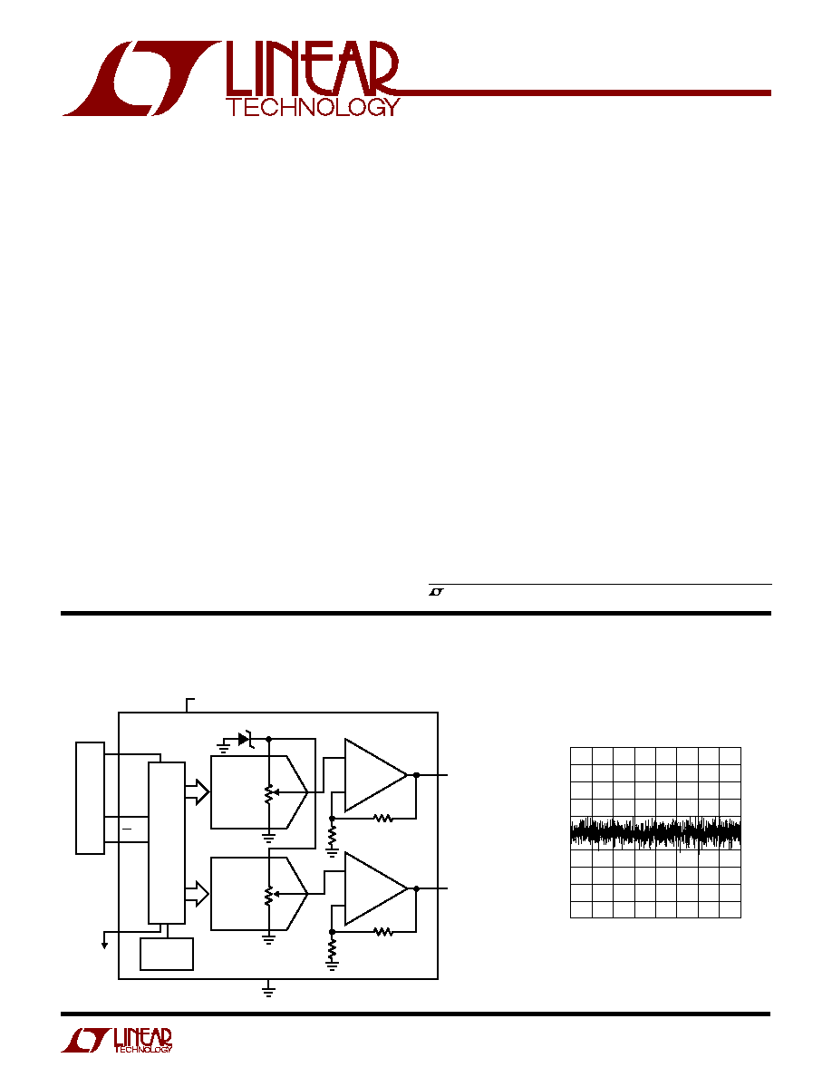
TYPICAL APPLICATIO
N
U
Dual 12-Bit Rail-to-Rail
Micropower DACs in SO-8
s
Dual DACs with 12-Bit Resolution
s
SO-8 Package
s
Rail-to-Rail Output Amplifiers
s
Internal Reference
s
Maximum DNL Error: 0.5LSB
s
3V Operation (LTC1446L): I
CC
= 650
µ
A Typ
s
5V Operation (LTC1446): I
CC
= 1000
µ
A Typ
s
Settling Time: 14
µ
s to
±
0.5LSB
s
Power-On Reset Clears DACs to 0V
s
3-Wire Cascadable Serial Interface with 500kHz
Update Rate
s
Schmitt Trigger On Input Allows Direct
Optocoupler Interface
s
Low Cost
The LTC
®
1446/LTC1446L are dual 12-bit digital-to-analog
converters (DACs) available in an SO-8 package. They are
complete with a rail-to-rail voltage output amplifier, an
internal reference and an easy-to-use 3-wire cascadable
serial interface.
The LTC1446 has an internal reference and a full-scale
output of 4.095V. It operates from a single 4.5V to 5.5V
supply.
The LTC1446L has an internal reference and a full-scale
output of 2.5V. It operates from a single 2.7V to 5.5V
supply.
The low power supply current makes the LTC1446 family
ideal for battery-powered applications. These DACs are
available in space saving 8-pin SO and PDIP packages and
require no external components for operation.
Differential Nonlinearity vs Input Code
CODE
0
0.5
DNL ERROR (LSB)
0.4
0.2
0.1
0
0.5
0.2
1024
2048 2560
1446/46L G13
0.3
0.3
0.4
0.1
512
1536
3072 3584 4095
+
+
12-BIT
DAC B
LTC1446: 5V
LTC1446L: 3V TO 5V
RAIL-TO-RAIL
VOLTAGE
OUTPUT
12-BIT
DAC A
POWER-ON
RESET
24-BIT
SHIFT
REG
AND
DAC
LATCH
µ
P
D
IN
2
7
D
OUT
4
6
1446/1446L TA01
CLK
1
CS/LD
3
8
V
OUT B
5
V
OUT A
V
CC
GND
Functional Block Diagram: Dual 12-Bit Rail-to-Rail DAC
s
Digital Calibration
s
Industrial Process Control
s
Automatic Test Equipment
s
Cellular Telephones
, LTC and LT are registered trademarks of Linear Technology Corporation.
2
LTC1446/LTC1446L
A
U
G
W
A
W
U
W
A
R
BSOLUTE
XI
TI
S
V
CC
to GND ................................................ 0.5 to 7.5V
Logic Inputs to GND ................................... 0.5 to 7.5V
Operating Temperature Range
LTC1446C/LTC1446LC ............................ 0
°
C to 70
°
C
LTC1446I/LTC1446LI .......................... 40
°
C to 85
°
C
V
OUT A
/V
OUT B
................................. 0.5V to V
CC
+ 0.5V
Maximum Junction Temperature .......................... 125
°
C
Storage Temperature Range ..................65
°
C to 150
°
C
Lead Temperature (Soldering, 10 sec)................. 300
°
C
PACKAGE/ORDER I
N
FOR
M
ATIO
N
W
U
U
ORDER PART
NUMBER
LTC1446CS8
LTC1446IS8
LTC1446LCS8
LTC1446LIS8
S8 PART MARKING
1446
1446L
1446I
1446LI
ORDER PART
NUMBER
LTC1446CN8
LTC1446IN8
LTC1446LCN8
LTC1446LIN8
T
JMAX
= 125
°
C,
JA
= 100
°
C/W
T
JMAX
= 125
°
C,
JA
= 150
°
C/W
1
2
3
4
8
7
6
5
TOP VIEW
V
OUT B
V
CC
GND
V
OUT A
CLK
D
IN
CS/LD
D
OUT
N8 PACKAGE
8-LEAD PDIP
Consult factory for Military grade parts.
ELECTRICAL CHARACTERISTICS
1
2
3
4
8
7
6
5
TOP VIEW
V
OUT B
V
CC
GND
V
OUT A
CLK
D
IN
CS/LD
D
OUT
S8 PACKAGE
8-LEAD PLASTIC SO
SYMBOL
PARAMETER
CONDITIONS
MIN
TYP
MAX
UNITS
DAC
Resolution
q
12
Bits
DNL
Differential Nonlinearity
Guaranteed Monotonic (Note 2)
q
±
0.2
±
0.5
LSB
INL
Integral Nonlinearity
T
A
= 25
°
C
±
2.0
4.5
LSB
q
±
2.5
5.0
LSB
ZSE
Zero-Scale Error
q
0
3
18
mV
V
OS
Offset Error
q
±
2
±
18
mV
V
OS
TC
Offset Error Tempco
±
15
µ
V/
°
C
V
FS
Full-Scale Voltage
LTC1446, T
A
= 25
°
C
4.065
4.095
4.125
V
LTC1446
q
4.045
4.095
4.145
V
LTC1446L, T
A
= 25
°
C
2.470
2.500
2.530
V
LTC1446L
q
2.460
2.500
2.540
V
V
FS
TC
Full-Scale Voltage Tempco
±
0.1
LSB/
°
C
Power Supply (LTC1446)
V
CC
Positive Supply Voltage
For Specified Performance
q
4.5
5.5
V
I
CC
Supply Current
4.5V
V
CC
5.5V (Note 5)
q
1000
1500
µ
A
Power Supply (LTC1446L)
V
CC
Positive Supply Voltage
For Specified Performance
q
2.7
5.5
V
I
CC
Supply Current
2.7V
V
CC
5.5V (Note 5)
q
650
1000
µ
A
The
q
denotes the specifications which apply over the full operating
temperature range. V
CC
= 4.5V to 5.5V (LTC1446), 2.7V to 5.5V (LTC1446L), V
OUT A
and V
OUT B
unloaded, T
A
= T
MIN
to T
MAX,
unless
otherwise noted.
(Note 1)
3
LTC1446/LTC1446L
The
q
denotes the specifications which apply over the full operating temperature range. V
CC
= 4.5V to 5.5V (LTC1446), 2.7V to 5.5V
(LTC1446L), V
OUT A
and V
OUT B
unloaded, T
A
= T
MIN
to T
MAX,
unless otherwise noted.
ELECTRICAL CHARACTERISTICS
The
q
denotes the specifications which apply over the full operating temperature range.V
CC
= 5V (LTC1446), V
CC
= 3V (LTC1446L),
T
A
= T
MIN
to T
MAX,
unless otherwise noted.
SYMBOL
PARAMETER
CONDITIONS
MIN
TYP
MAX
UNITS
Op Amp DC Performance
Short-Circuit Current Low
V
OUT
Shorted to GND
q
55
120
mA
Short-Circuit Current High
V
OUT
Shorted to V
CC
q
70
120
mA
Output Impedance to GND
Input Code = 0
q
40
160
AC Performance
Voltage Output Slew Rate
(Note 3)
q
0.5
1
V/
µ
s
Voltage Output Settling Time
(Notes 3, 4) to
±
0.5LSB
14
µ
s
Note 1: Absolute Maximum Ratings are those values beyond which the life
of a device may be impaired.
Note 2: Nonlinearity is defined from the first code that is greater than or
equal to the maximum offset specification to code 4095 (full scale).
Note 3: Load is 5k
in parallel with 100pF.
Note 4: DAC switched between all 1s and the code corresponding to V
OS
for the part.
Note 5: Digital inputs at 0V or V
CC
.
LTC1446
LTC1446L
SYMBOL
PARAMETER
CONDITIONS
MIN
TYP
MAX
MIN
TYP
MAX
UNITS
Digital I/O
V
IH
Digital Input High Voltage
q
2.4
2
V
V
IL
Digital Input Low Voltage
q
0.8
0.6
V
V
OH
Digital Output High Voltage
I
OUT
= 1mA
q
V
CC
1.0
V
CC
0.7
V
V
OL
Digital Output Low Voltage
I
OUT
= 1mA
q
0.4
0.4
V
I
LEAK
Digital Input Leakage
V
IN
= GND to V
CC
q
±
10
±
10
µ
A
C
IN
Digital Input Capacitance
Guaranteed by Design
q
10
10
pF
Switching
t
1
D
IN
Valid to CLK Setup
q
40
60
ns
t
2
D
IN
Valid to CLK Hold
q
0
0
ns
t
3
CLK High Time
q
40
60
ns
t
4
CLK Low Time
q
40
60
ns
t
5
CS/LD Pulse Width
q
50
80
ns
t
6
LSB CLK to CS/LD
q
40
60
ns
t
7
CS/LD Low to CLK
q
20
30
ns
t
8
D
OUT
Output Delay
C
LOAD
= 15pF
q
150
220
ns
t
9
CLK Low to CS/LD Low
q
20
30
ns
4
LTC1446/LTC1446L
TYPICAL PERFOR
M
A
N
CE CHARACTERISTICS
U
W
CODE
0
0.5
DNL ERROR (LSB)
0.4
0.2
0.1
0
0.5
0.2
1024
2048 2560
1446/46L G01
0.3
0.3
0.4
0.1
512
1536
3072 3584 4095
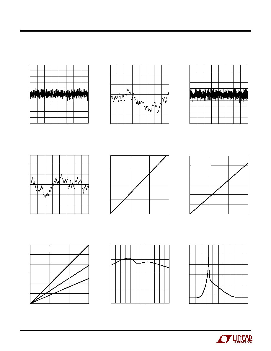
LTC1446 Differential Nonlinearity
(DNL)
LTC1446 Integral Nonlinearity (INL)
LTC1446L Differential Nonlinearity
LTC1446L Integral Nonlinearity
LTC1446 Min Supply Headroom for
Full Output Swing vs Load Current
LTC1446L Min Supply Headroom for
Full Output Swing vs Load Current
LTC1446 Full-Scale Voltage
vs Temperature
TEMPERATURE (
°
C)
55
4.07
FULL-SCALE VOLTAGE (V) 4.08
4.09
4.10
4.11
25
5
35
65
1446/46L G09
95
125
CODE
0
3
INL ERROR (LSB)
2
1
0
1
1024
2048
3072
4095
1446/46L G02
2
3
512
1536
2560
3584
CODE
0
0.5
DNL ERROR (LSB)
0.4
0.2
0.1
0
0.5
0.2
1024
2048 2560
1446/46L G03
0.3
0.3
0.4
0.1
512
1536
3072 3584 4095
CODE
0
3
INL ERROR (LSB)
2
1
0
1
1024
2048
3072
4095
1446/46L G04
2
3
512
1536
2560
3584
LOAD CURRENT (mA)
0
V
CC
V
OUT
(V)
0.4
0.6
15
LTC1446/46L · TPC05
0.2
0
5
10
0.8
V
OUT
< 1LSB
CODE: ALL 1's
V
OUT
= 4.095V
LOAD CURRENT (mA)
0
0
V
CC
V
OUT
0.2
0.4
0.6
0.8
1.2
5
10
LTC1446/46L · TPC06
15
1.0
V
OUT
< 1LSB
CODE: ALL 1's
V
OUT
= 2.5V
OUTPUT SINK CURRENT (mA)
0
0
OUTPUT PULL-DOWN VOLTAGE (mV)
100
200
300
400
600
5
10
LTC1446/46L · TPC07
15
500
CODE: ALL 0'S
125
°
C
25
°
C
55
°
C
LTC1446 Min Output Voltage vs
Output Sink Current
LTC1446 Supply Current
vs Logic Input Voltage
LOGIC INPUT VOLTAGE (V)
0.6
SUPPLY CURRENT (mA)
1.4
2.2
3.0
1.0
1.8
2.6
1
2
3
4
1446/46L G09
5
0
5
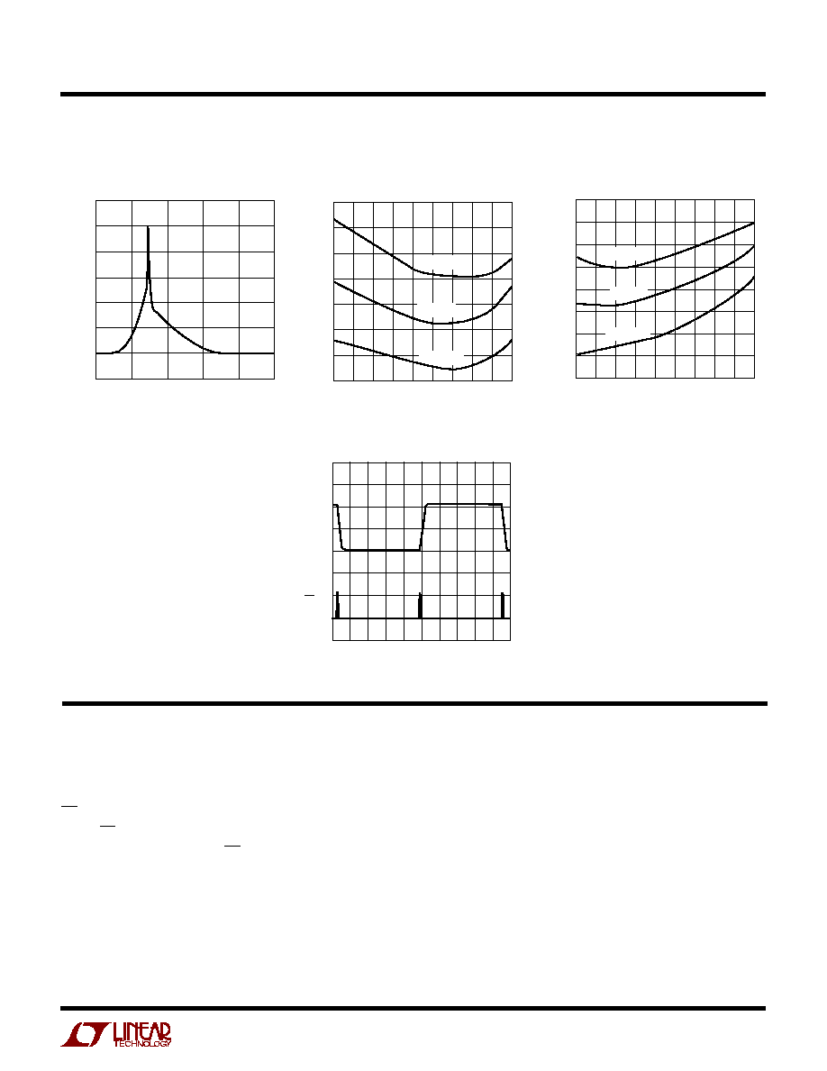
LTC1446/LTC1446L
1446L G13
TIME (10
µ
s/DIV)
V
OUT
(2V/DIV)
CS/LD
(5V/DIV)
TYPICAL PERFOR
M
A
N
CE CHARACTERISTICS
U
W
LTC1446L Supply Current vs Logic
Input Voltage
LOGIC INPUT VOLTAGE (V)
0.5
1.0
1.1
1.2
1446/46L G10
0.9
0.8
1.0
1.5
2.0
2.5
3.0
0.7
0.6
0.5
SUPPLY CURRENT (mA)
LTC1446 Supply Current vs
Temperature
TEMPERATURE (
°
C)
55
SUPPLY CURRENT (
µ
A)
660
670
680
105
1446/46L G12
650
640
620
15
25
65
35
125
5
45
85
630
700
690
V
CC
= 3.3V
V
CC
= 2.7V
V
CC
= 3V
LTC1446L Supply Current
vs Temperature
PI
N
FU
N
CTIO
N
S
U
U
U
CLK: The Serial Interface Clock.
D
IN
: The Serial Interface Data.
CS/LD: The Serial Interface Enable and Load Control.
When CS/LD is low the CLK signal is enabled, so the data
can be clocked in. When CS/LD is pulled high data is
loaded from the shift register into the DAC registers,
updating the DAC outputs.
D
OUT
: The output of the shift register which becomes valid
on the rising edge of the serial clock.
GND: Ground.
V
OUT A
,V
OUT B
: Buffered DAC Outputs.
V
CC
: Positive Supply Input.
4.5V
V
CC
5.5V (LTC1446), 2.7V
V
CC
5.5V
(LTC1446L). Requires a 0.1
µ
F bypass capacitor to
ground.
TEMPERATURE (
°
C)
55 35 15
5
25
45
65
85 105
900
SUPPLY CURRENT (
µ
A)
910
930
940
970
1446/46L G11
920
125
950
960
V
CC
= 5.5V
V
CC
= 4.5V
V
CC
= 5V
Large Signal Transient Response