Äîêóìåíòàöèÿ è îïèñàíèÿ www.docs.chipfind.ru
1
LTC1448
Dual 12-Bit Rail-to-Rail
Micropower DAC
+
+
12-BIT
DAC B
RAIL-TO-RAIL
VOLTAGE
OUTPUTS
12-BIT
DAC A
POWER-ON
RESET
24-BIT
SHIFT
REG
AND
DAC
LATCH
µ
P
D
IN
2
7
REF
4
6
1448 TA01
CLK
1
CS/LD
3
8
V
OUT B
5
V
OUT A
V
CC
GND
2.7V TO 5.5V
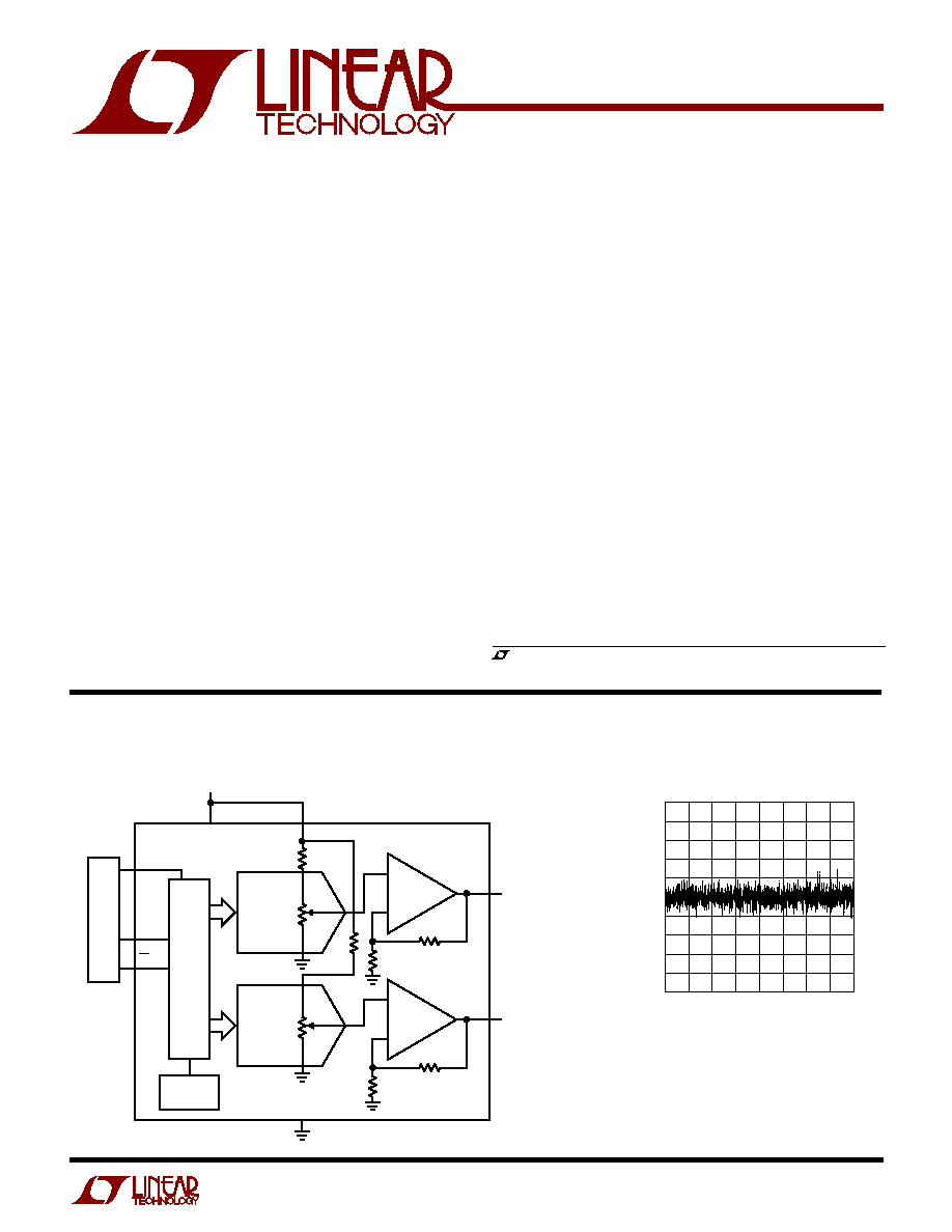
Functional Block Diagram: 12-Bit Rail-to-Rail Dual DAC
Differential Nonlinearity
vs Input Code
CODE
0
0.5
DNL ERROR (LSB)
0.4
0.2
0.1
0
0.5
0.2
1024
2048 2560
1448 TA02
0.3
0.3
0.4
0.1
512
1536
3072 3584 4095
FEATURES
s
SO-8 Package
s
12-Bit Resolution
s
Buffered True Rail-to-Rail Voltage Output
s
External Reference Input Can Be Tied to V
CC
s
Output Swings from 0V to V
REF
s
3V and 5V Supply Operation
s
Schmitt Trigger on Clock Input Allows Direct
Optocoupler Interface
s
Power-On Reset Clears DACs to 0V
s
3-Wire Serial Interface
s
Maximum DNL Error: 0.5LSB
s
Low Cost
The LTC
®
1448 is a dual rail-to-rail voltage output, 12-bit
digital-to-analog converter (DAC). It includes rail-to-rail
output buffer amplifiers and an easy-to-use 3-wire serial
interface. It is available in 8-pin SO and PDIP packages and
provides the smallest footprint of any dual 12-bit DAC.
The LTC1448 has an external reference input pin (REF)
and its outputs swing from 0V to REF. The REF input can
be tied to V
CC
providing rail-to-rail operation from supplies
of 2.7V to 5.5V. (For devices with internal reference see the
LTC1446 data sheet.) The LTC1448 dissipates 2.5mW
from a 5V supply.
The low power supply current and the small SO-8 package
make the LTC1448 ideal for battery-powered applications.
DESCRIPTIO
N
U
, LTC and LT are registered trademarks of Linear Technology Corporation.
s
Digital Calibration
s
Industrial Process Control
s
Automatic Test Equipment
s
Cellular Telephones
APPLICATIO
N
S
U
TYPICAL APPLICATIO
N
U
2
LTC1448
ABSOLUTE
M
AXI
M
U
M
RATINGS
W
W
W
U
V
CC
to GND .............................................. 0.5V to 7.5V
Logic Inputs to GND ................................ 0.5V to 7.5V
V
OUT A
, V
OUT B
, REF to GND ........... 0.5V to V
CC
+ 0.5V
Maximum Junction Temperature .......................... 125°C
Operating Temperature Range
LTC1448C ............................................ 0°C to 70°C
LTC1448I......................................... 40°C to 85°C
Storage Temperature Range ................ 65°C to 150°C
Lead Temperature (Soldering, 10 sec)................. 300°C
W
U
U
PACKAGE/ORDER I FOR ATIO
ORDER PART
NUMBER
LTC1448CN8
LTC1448IN8
LTC1448CS8
LTC1448IS8
S8 PART MARKING
1448
1448I
Consult factory for Military grade parts.
ELECTRICAL CHARACTERISTICS
V
CC
= 2.7V to 5.5V, V
OUT A
and V
OUT B
unloaded, REF
V
CC
, T
A
= T
MIN
to T
MAX
, unless otherwise noted.
1
2
3
4
8
7
6
5
TOP VIEW
CLK
D
IN
CS/LD
REF
V
OUT B
V
CC
GND
V
OUT A
S8 PACKAGE
8-LEAD PLASTIC SO
N8 PACKAGE
8-LEAD PDIP
T
JMAX
= 125°C,
JA
= 100°C/W (N8)
T
JMAX
= 125°C,
JA
= 150°C/W (S8)
SYMBOL
PARAMETER
CONDITIONS
MIN
TYP
MAX
UNITS
DAC
Resolution
q
12
Bits
Monotonicity
q
12
Bits
DNL
Differential Nonlinearity
V
REF
V
CC
0.1V (Note 1)
q
± 0.2
± 0.5
LSB
INL
Integral Nonlinearity
V
REF
V
CC
0.1V (Note 1), T
A
= 25°C
± 5.0
LSB
V
REF
V
CC
0.1V (Note 1)
q
± 5.5
LSB
V
OS
Offset Error
Measured at Code 20, T
A
= 25°C
± 10
mV
Measured at Code 20
q
± 15
mV
V
OS
TC
Offset Error Temperature
±15
µV/°C
Coefficient
V
FS
Full-Scale Voltage
V
REF
= 4.096V, T
A
= 25°C
4.070
4.095
4.120
V
V
REF
= 4.096V
q
4.060
4.095
4.130
V
V
FS
TC
Full-Scale Voltage
10
ppm/°C
Temperature Coefficient
Power Supply
V
CC
Positive Supply Voltage
For Specified Performance
q
2.7
5.5
V
I
CC
Supply Current
(Note 4)
q
450
700
µA
Op Amp DC Performance
Short-Circuit Current Low
V
OUT
Shorted to GND
q
55
120
mA
Short-Circuit Current High
V
OUT
Shorted to V
CC
q
65
120
mA
Output Impedance to GND
Input Code = 0
q
30
120
Output Line Regulation
Input Code = 4095. V
CC
= 4.5V to 5.5V, V
REF
= 4.096V
q
0.2
1.5
LSB/V
3
LTC1448
V
CC
= 2.7V to 5.5V, V
OUT A
and V
OUT B
unloaded, REF
V
CC
, T
A
= T
MIN
to T
MAX
, unless otherwise noted.
ELECTRICAL CHARACTERISTICS
Note 4: Digital inputs at 0V or V
CC
.
Note 5: V
OUT
can only swing from (GND +
V
OS
) to (V
CC
V
OS
) when
output is unloaded.
Note 6. Guaranteed by design, not subject to test.
SYMBOL
PARAMETER
CONDITIONS
MIN
TYP
MAX
UNITS
AC Performance
Voltage Output Slew Rate
q
0.5
1.0
V/µs
Voltage Output Settling Time
(Notes 2, 3) to ± 0.5LSB
14
µs
Digital Feedthrough
0.3
nV · s
Reference Input
R
IN
REF Input Resistance
q
7.5
12.5
18
k
REF
REF Input Range
(Notes 5, 6)
q
0
V
CC
V
Digital I/O
V
IH
Digital Input High Voltage
V
CC
= 5V
q
2.4
V
V
CC
= 3V
q
2.0
V
V
IL
Digital Input Low Voltage
V
CC
= 5V
q
0.8
V
V
CC
= 3V
q
0.6
V
I
LEAK
Digital Input Leakage
V
IN
= GND to V
CC
q
± 10
µA
C
IN
Digital Input Capacitance
(Note 6)
q
10
pF
Switching (V
CC
= 4.5V to 5.5V)
t
1
D
IN
Valid to CLK Setup
q
40
ns
t
2
D
IN
Valid to CLK Hold
q
0
ns
t
3
CLK High Time
(Note 6)
q
40
ns
t
4
CLK Low Time
(Note 6)
q
40
ns
t
5
CS/LD Pulse Width
(Note 6)
q
50
ns
t
6
LSB CLK to CS/LD
(Note 6)
q
40
ns
t
7
CS/LD Low to CLK
(Note 6)
q
20
ns
t
8
CLK Low to CS/LD Low
(Note 6)
q
20
ns
Switching (V
CC
= 2.7V to 5.5V)
t
1
D
IN
Valid to CLK Setup
q
60
ns
t
2
D
IN
Valid to CLK Hold
q
0
ns
t
3
CLK High Time
(Note 6)
q
60
ns
t
4
CLK Low Time
(Note 6)
q
60
ns
t
5
CS/LD Pulse Width
(Note 6)
q
80
ns
t
6
LSB CLK to CS/LD
(Note 6)
q
60
ns
t
7
CS/LD Low to CLK
(Note 6)
q
30
ns
t
8
CLK Low to CS/LD Low
(Note 6)
q
30
ns
The
q
denotes specifications which apply over the full operating
temperature range.
Note 1: Nonlinearity is defined from code 20 to code 4095 (full scale).
See Applications Information.
Note 2: Load is 5k in parallel with 100pF.
Note 3: DAC switched between all 1s and the code corresponding to V
OS
for the part.
4
LTC1448
CLK (Pin 1): Serial Interface Clock. Internal Schmitt trig-
ger on this input allows direct optocoupler interface.
D
IN
(Pin 2): Serial Interface Data. Data on the D
IN
pin is
latched into the shift register on the rising edge of the serial
clock.
CS/LD (Pin 3): Serial Interface Enable and Load Control.
When CS/LD is low the CLK signal is enabled, so the data
can be clocked in. When CS/LD is pulled high, data is
loaded from the shift register into the DAC register,
PI
N
FU
N
CTIO
N
S
U
U
U
updating the DAC output and the CLK is disabled
internally.
REF (Pin 4): Reference Input for Both DACs. This pin can
be tied to V
CC
. The output will swing from 0V to REF. The
typical input resistance is 12.5k.
V
OUT A
, V
OUT B
(Pins 5, 8): Buffered DAC Outputs.
GND (Pin 6): Ground.
V
CC
(Pin 7): Positive Supply Input. 2.7V
V
CC
5.5V.
Requires a bypass capacitor to ground.
TYPICAL PERFOR
M
A
N
CE CHARACTERISTICS
U
W
LOAD CURRENT (mA)
0
V
CC
V
OUT
(V)
5
10
15
1448 G03
0.8
0.7
0.6
0.5
0.4
0.3
0.2
0.1
0
V
OUT
< 1LSB
CODE: ALL 1's
V
OUT
= 4.095V
OUTPUT SINK CURRENT (mA)
0
OUTPUT PULL-DOWN VOLTAGE (mV)
5
10
15
1448 G04
800
700
600
500
400
300
200
100
0
CODE: ALL 0's
125
°
C
25
°
C
55
°
C
Integral Nonlinearity (INL)
Minimum Supply Headroom for
Full Output Swing vs Load Current
Minimum Output Voltage vs
Output Sink Current
Supply Current vs
Logic Input Voltage
Differential Nonlinearity (DNL)
CODE
0
INL ERROR (LSB)
5
4
3
2
1
0
1
2
3
4
5
1024
2048 2560
1448 G01
512
1536
3072 3584 4095
CODE
0
0.5
DNL ERROR (LSB)
0.4
0.2
0.1
0
0.5
0.2
1024
2048 2560
1448 TA02
0.3
0.3
0.4
0.1
512
1536
3072 3584 4095
LOGIC INPUT VOLTAGE (V)
0
SUPPLY CURRENT (mA)
2.0
1.6
1.2
0.8
0.4
0
4
1448 G06
1
2
3
5
5
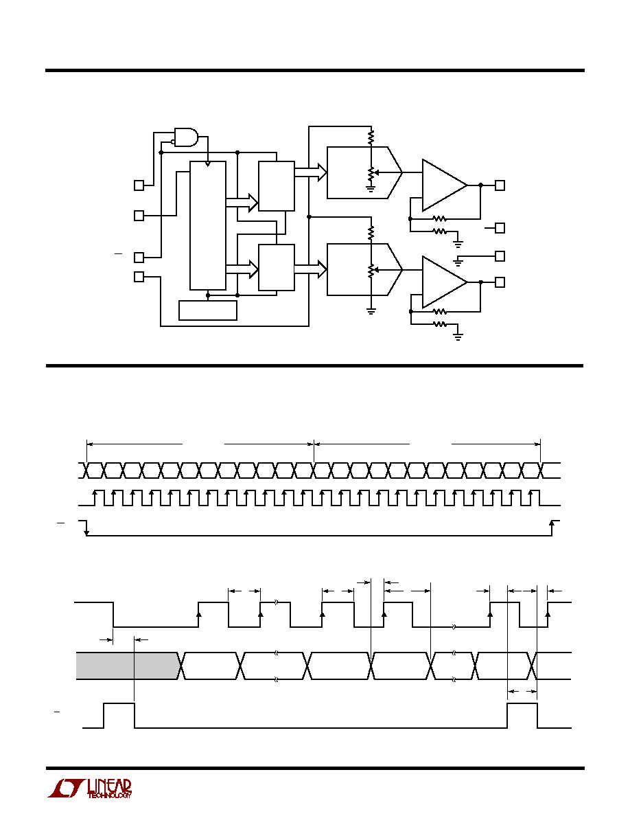
LTC1448
W
I
D AGRA
BLOCK
24-BIT
SHIFT
REGISTER
POWER-ON
RESET
LD
DAC B
REGISTER
LD
DAC A
REGISTER
12-BIT
DAC A
+
+
8
V
OUT B
7
V
CC
6
GND
5
V
OUT A
12-BIT
DAC B
1
2
3
4
CLK
D
IN
CS/LD
REF
1448 BD
TI I G DIAGRA S
U
W
W
CLK
D
IN
CS/LD
t
8
t
4
t
3
t
5
B11-A
MSB
B0-A
LSB
B11-B
MSB
B0-B
LSB
t
2
t
1
t
6
t
7
B0-B
PREVIOUS WORD
1448 TD02
D
IN
CLK
CS/LD
1
2
3
4
5
6
7
8
9
10
11
12
13
14
15
16
17
18
19
20
21
22
23
24
DAC B INPUT
DAC A INPUT
1448 TD01
D11
D9
D8
D7
D6
D5
D4
D3
D2
D1
D0
D10
D11
D9
D8
D7
D6
D5
D4
D3
D2
D1
D0
D10
(UPDATE DAC OUTPUT)
(ENABLE CLOCK)
OPERATING SEQUENCE
MSB
MSB
LSB
LSB