Äîêóìåíòàöèÿ è îïèñàíèÿ www.docs.chipfind.ru
1
LTC1456
12-Bit Rail-to-Rail
Micropower DAC
with Clear Input
s
Digital Calibration
s
Industrial Process Control
s
Automatic Test Equipment
s
Cellular Telephones
APPLICATIO
N
S
U
TYPICAL APPLICATIO
N
U
CODE
0
DNL ERROR (LSB)
0.5
0
0.5
1024
2048 2560
1456 TA02
512
1536
3072 3584 4095
Differential Nonlinearity
vs Input Code
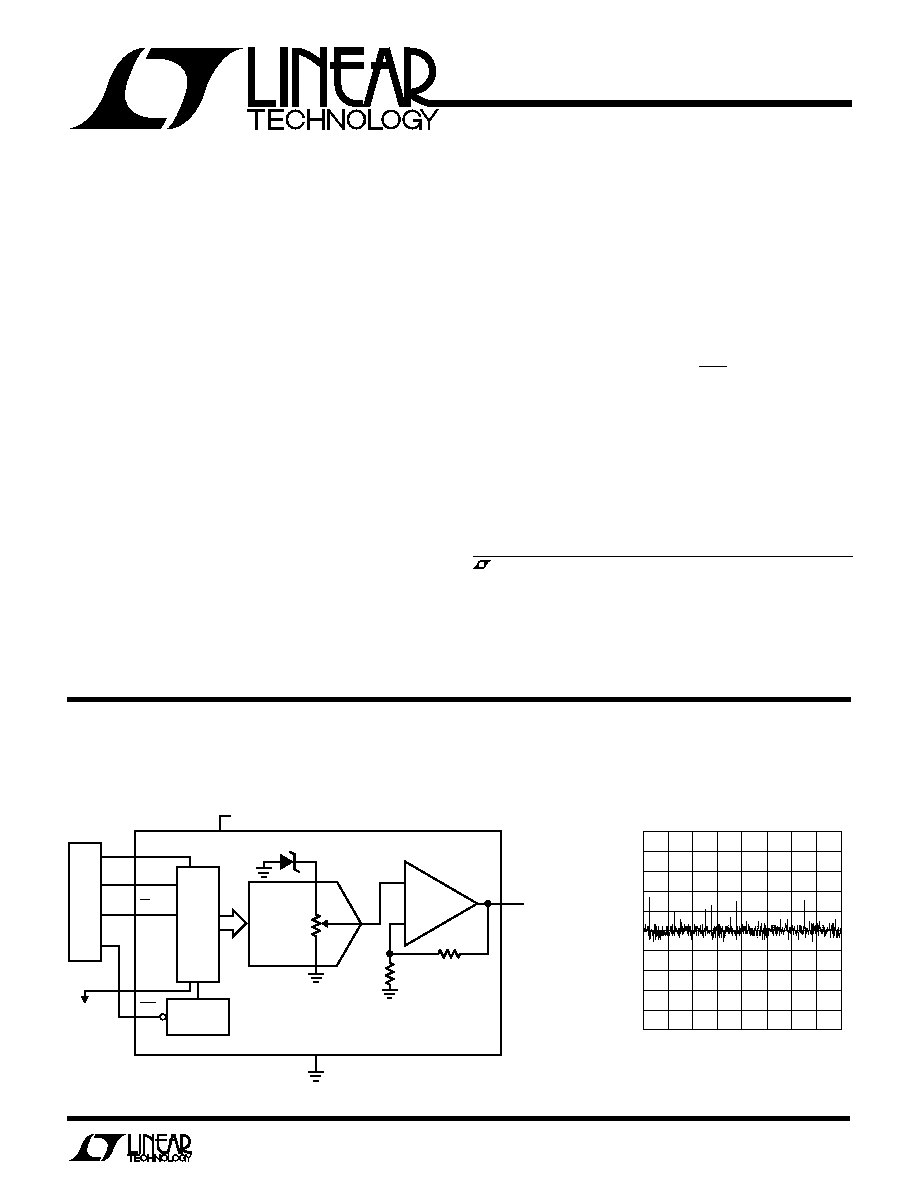
Functional Block Diagram: 12-Bit Rail-to-Rail DAC with Clear Input
+
12-BIT
DAC
4.5V TO 5.5V
2.048V
GND
POWER-ON
RESET
TO
OTHER
DACS
12-BIT
SHIFT
REG
AND
DAC
LATCH
µ
P
D
IN
V
CC
2
8
D
OUT
4
5
1456 TA01
CLK
1
CS/LD
3
CLR
6
7
RAIL-TO-RAIL
VOLTAGE
OUTPUT
V
OUT
FEATURES
s
SO-8 Package
s
12-Bit Resolution
s
Buffered True Rail-to-Rail Voltage Output
s
Asynchronous Clear Input
s
Built-In Reference
s
Schmitt Trigger On Clock Input Allows Direct
Optocoupler Interface
s
Power-On Reset Clears DAC to 0V
s
3-Wire Cascadable Serial Interface
s
Maximum DNL Error: 0.5LSB
s
Low Cost
The LTC
®
1456 is a complete single supply, rail-to-rail
voltage output, 12-bit digital-to-analog converter (DAC) in
an SO-8 package. It includes a rail-to-rail output buffer
amplifier and an easy-to-use 3-wire cascadable serial
interface. The LTC1456 includes a CLR pin that asynchro-
nously clears the DAC to zero scale.
The LTC1456 has an internal 2.048V reference and a full-
scale output of 4.095V. It operates on a 4.5V to 5.5V
supply, dissipating 2.2mW.
The low power supply current and the space saving SO-8
package make the LTC1456 ideal for battery-powered
applications.
DESCRIPTIO
N
U
, LTC and LT are registered trademarks of Linear Technology Corporation.
2
LTC1456
ABSOLUTE
M
AXI
M
U
M
RATINGS
W
W
W
U
W
U
U
PACKAGE/ORDER I FOR ATIO
ORDER PART
NUMBER
LTC1456CN8
LTC1456IN8
LTC1456CS8
LTC1456IS8
S8 PART MARKING
1456
1456I
V
CC
to GND .............................................. 0.5V to 7.5V
Logic Inputs to GND ................................ 0.5V to 7.5V
V
OUT
.............................................. 0.5V to V
CC
+ 0.5V
Maximum Junction Temperature ......... 65
°
C to 125
°
C
Operating Temperature Range
LTC1456C ............................................ 0
°
C to 70
°
C
LTC1456I ........................................ 40
°
C to 85
°
C
Storage Temperature Range ................ 65
°
C to 150
°
C
Lead Temperature (Soldering, 10 sec)................. 300
°
C
Consult factory for Military grade parts.
T
JMAX
= 125
°
C,
JA
= 100
°
C/W (N8)
T
JMAX
= 125
°
C,
JA
= 150
°
C/W (S8)
1
2
3
4
8
7
6
5
TOP VIEW
CLK
D
IN
CS/LD
D
OUT
V
CC
V
OUT
CLR
GND
N8 PACKAGE
8-LEAD PDIP
S8 PACKAGE
8-LEAD PLASTIC SO
ELECTRICAL CHARACTERISTICS
V
CC
= 4.5V to 5.5V, V
OUT
unloaded, T
A
= T
MIN
to T
MAX
, unless otherwise noted.
SYMBOL
PARAMETER
CONDITIONS
MIN
TYP
MAX
UNITS
DAC
Resolution
q
12
Bits
DNL
Differential Nonlinearity
Guaranteed Monotonic (Note 1)
q
±
0.5
LSB
INL
Integral Nonlinearity
T
A
= 25
°
C
±
3.5
LSB
(Note 1)
q
±
4
LSB
V
OS
Offset Error
T
A
= 25
°
C
±
12
mV
q
±
18
mV
V
OS
TC
Offset Error Temperature
±
15
µ
V/
°
C
Coefficient
V
FS
Full-Scale Voltage
T
A
= 25
°
C
4.065
4.095
4.125
V
q
4.045
4.095
4.145
V
V
FS
TC
Full-Scale Voltage
±
24
ppm/
°
C
Temperature Coefficient
Power Supply
V
CC
Positive Supply Voltage
For Specified Performance
q
4.5
5.5
V
I
CC
Supply Current
(Note 4)
q
430
650
µ
A
Op Amp DC Performance
Short-Circuit Current Low
V
OUT
Shorted to GND
q
120
mA
Short-Circuit Current High
V
OUT
Shorted to V
CC
q
120
mA
Output Impedance to GND
Input Code = 0
q
40
120
AC Performance
Voltage Output Slew Rate
(Note 2)
q
0.4
1.0
V/
µ
s
Voltage Output Settling Time
(Notes 2, 3) to
±
0.5LSB
14
µ
s
Digital Feedthrough
0.3
nV · s
3
LTC1456
V
CC
= 4.5V to 5.5V, V
OUT
unloaded, T
A
= T
MIN
to T
MAX
, unless otherwise noted.
ELECTRICAL CHARACTERISTICS
The
q
denotes specifications which apply over the full operating
temperature range.
Note 1: Nonlinearity is defined from the first code that is greater than or
equal to the maximum offset specification to code 4095 (full scale).
Note 2: Load is 5k
in parallel with 100pF.
Note 3: DAC switched between all 1s and the code corresponding to V
OS
for the part.
Note 4: Digital inputs at 0V or V
CC
.
SYMBOL
PARAMETER
CONDITIONS
MIN
TYP
MAX
UNITS
Digital I/O
V
IH
Digital Input High Voltage
q
2.4
V
V
IL
Digital Input Low Voltage
q
0.8
V
V
OH
Digital Output High Voltage
I
OUT
= 1mA, D
OUT
Only
q
V
CC
1.0
V
V
OL
Digital Output Low Voltage
I
OUT
= 1mA, D
OUT
Only
q
0.4
V
I
LEAK
Digital Input Leakage
V
CC
= 5V, V
IN
= GND to V
CC
q
±
10
µ
A
C
IN
Digital Input Capacitance
Guaranteed by Design. Not Subject to Test.
q
10
pF
Switching
t
1
D
IN
Valid to CLK Setup
q
40
ns
t
2
D
IN
Valid to CLK Hold
q
0
ns
t
3
CLK High Time
q
40
ns
t
4
CLK Low Time
q
40
ns
t
5
CS/LD Pulse Width
q
50
ns
t
6
LSB CLK to CS/LD
q
40
ns
t
7
CS/LD Low to CLK
q
20
ns
t
8
D
OUT
Output Delay
C
LOAD
= 15pF, V
CC
= 5V
q
150
ns
t
9
CLK Low to CS/LD Low
q
20
ns
t
10
CLR Pulse Width
q
65
ns
4
LTC1456
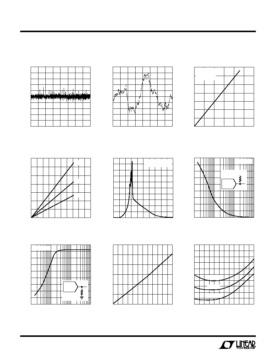
TYPICAL PERFOR
M
A
N
CE CHARACTERISTICS
U
W
CODE
0
0.5
DNL (LSB)
0.4
0.2
0.1
0
0.5
0.2
1024
2048 2560
1456 G01
0.3
0.3
0.4
0.1
512
1536
3072 3584 4095
Differential Nonlinearity (DNL)
Minimum Supply Headroom for
Full Output Swing vs Load Current
LOAD CURRENT (mA)
0
0.8
1.0
1.2
15
25
1456 G03
0.6
0.4
5
10
20
30
0.2
0
V
CC
V
OUT
(V)
1.4
V
OUT
< 1LSB
CODE: ALL 1s
V
OUT
= 4.095V
CODE
0
2.0
INL ERROR (LSB)
1.6
0.8
0.4
0
2.0
0.8
1024
2048 2560
1456 G02
1.2
1.2
1.6
0.4
512
1536
3072 3584 4095
Integral Nonlinearity (INL)
Minimum Output Voltage
vs Output Sink Current
OUTPUT SINK CURRENT (mA)
0
0
OUTPUT PULL-DOWN VOLTAGE (mV)
100
300
400
500
700
2
10
14
1456 G04
200
600
8
18 20
4
6
12
16
125
°
C
25
°
C
55
°
C
Supply Current
vs Logic Input Voltage
Output Swing vs Load Resistance
LOAD RESISTANCE (
)
10
2.5
OUTPUT SWING (V)
3.0
3.5
4.0
4.5
100
1k
10k
1456 G06
2.0
1.5
0.5
0
1.0
V
CC
R
L
CODE: ALL 0s
LOAD RESISTANCE (
)
10
2.5
OUTPUT SWING (V)
3.0
3.5
4.0
4.5
100
1k
10k
1456 G07
2.0
1.5
0.5
0
1.0
R
L
CODE: ALL 1s
Output Swing vs Load Resistance
Offset Voltage vs Temperature
TEMPERATURE (
°
C)
55
0.3
OFFSET VOLTAGE (mV)
0.4
0.5
0.6
0.7
0.9
25
5
35
65
1456 G08
95
125
0.8
Supply Current vs Temperature
TEMPERATURE (
°
C)
55
SUPPLY CURRENT (
µ
A)
510
530
550
65
1456 G09
490
470
500
520
540
480
460
450
25
5
35
95
125
V
CC
= 5.5V
V
CC
= 4.5V
V
CC
= 5V
LOGIC INPUT VOLTAGE (V)
0
SUPPLY CURRENT (mA)
1.210
1.480
1.750
4
1456 G05
0.940
0.670
1.075
1.345
1.615
0.805
0.535
0.400
1
2
3
0.5
4.5
1.5
2.5
3.5
5
ALL DIGITAL INPUTS
TIED TOGETHER
5
LTC1456
CLK (Pin 1): The Serial Interface Clock. Internal Schmitt
trigger on this input allows direct optocoupler interface.
D
IN
(Pin 2): The Serial Interface Data. Data on the D
IN
pin
is latched into the shift register on the rising edge of the
serial clock.
CS/LD (Pin 3): The Serial Interface Enable and Load
Control. When CS/LD is low the CLK signal is enabled, so
the data can be clocked in. When CS/LD is pulled high,
data is loaded from the shift register into the DAC
register, updating the DAC output. When CS/LD is high
the CLK is disabled internally.
PI
N
FU
N
CTIO
N
S
U
U
U
D
OUT
(Pin 4): The Output of the Shift Register Which
Becomes Valid on the Rising Edge of the Serial Clock.
GND (Pin 5): Ground.
CLR (Pin 6): The Clear Input. When pulled low, this pin
asynchronously clears the internal shift and DAC registers
to zero scale. Should be tied high for normal operation.
V
OUT
(Pin 7): The Buffered DAC Output.
V
CC
(Pin 8): The Positive Supply Input. 4.5V
V
CC
5.5V.
Requires a bypass capacitor to ground.
B11
MSB
B10
t
1
t
9
B1
t
6
B0
LSB
B11
CURRENT WORD
t
7
t
2
t
4
t
3
t
8
CLK
D
IN
D
OUT
CS/LD
t
5
1456 TD
B0
PREVIOUS WORD
B11
PREVIOUS WORD
B10
B1
B0
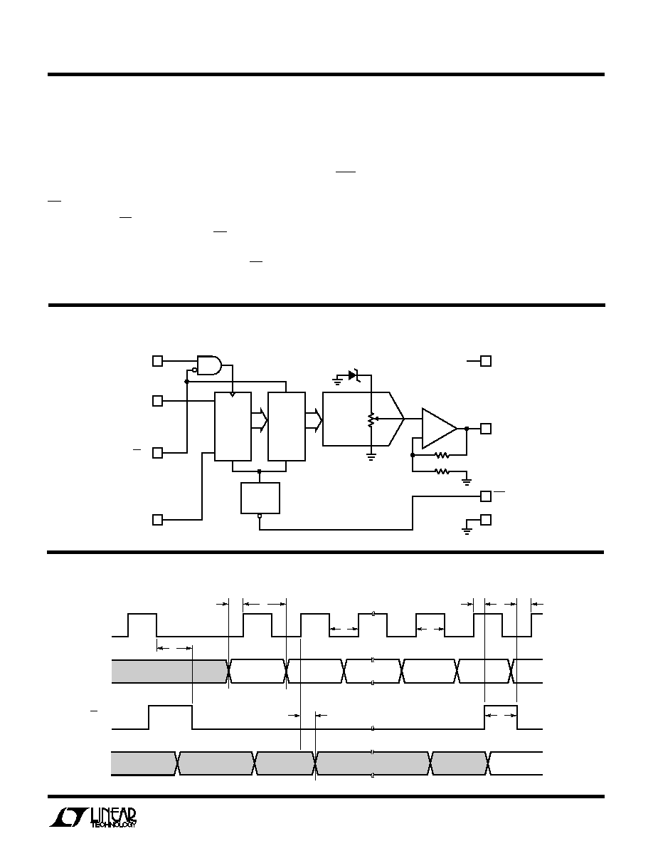
W
I
D AGRA
BLOCK
DAC
REGISTER
LD
12-BIT
SHIFT
REGISTER
POWER-ON
RESET
1146 BD
CLK 1
D
IN
2
D
OUT
4
V
OUT
7
CLR
6
GND
5
V
CC
8
3
CS/LD
12-BIT
DAC
2.048V
+
TI I G DIAGRA
W U
W