Äîêóìåíòàöèÿ è îïèñàíèÿ www.docs.chipfind.ru
1
LTC1474/LTC1475
Low Quiescent Current
High Efficiency Step-Down
Converters
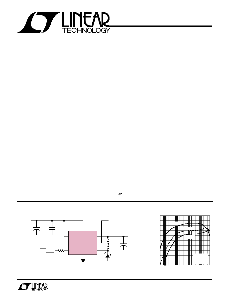
LOAD CURRENT (mA)
EFFICIENCY (%)
100
90
80
70
60
50
0.03
3
300
1474/75 TA01
0.3
30
V
IN
= 5V
V
IN
= 10V
V
IN
= 15V
L = 100
µ
H
V
OUT
= 3.3V
R
SENSE
= 0
LTC1474 Efficiency
Figure 1. High Efficiency Step-Down Converter
V
IN
GND
SENSE
LBI
RUN
V
FB
LBO
SW
LTC1474-3.3
+
6
3
8
1
2
5
7
4
100k
LOW BATTERY IN
RUN SHDN
0.1
µ
F
10
µ
F
25V
V
IN
4V TO 18V
LOW BATTERY OUT
1474/75 F01
L1
100
µ
H
D1
MBR0530
+
100
µ
F
6.3V
V
OUT
3.3V AT 250mA
L1 = SUMIDA CDRH74-101
FEATURES
DESCRIPTIO
N
U
s
High Efficiency: Over 92% Possible
s
Very Low Standby Current: 10
µ
A Typ
s
Available in Space Saving 8-Lead MSOP Package
s
Internal 1.4
Power Switch (V
IN
= 10V)
s
Wide V
IN
Range: 3V to 18V Operation
s
Very Low Dropout Operation: 100% Duty Cycle
s
Low-Battery Detector Functional During Shutdown
s
Programmable Current Limit with Optional
Current Sense Resistor (10mA to 400mA Typ)
s
Short-Circuit Protection
s
Few External Components Required
s
Active Low Micropower Shutdown: I
Q
= 6
µ
A Typ
s
Pushbutton On/Off (LTC1475 Only)
s
3.3V, 5V and Adjustable Output Versions
The LT C
®
1474/LTC1475 series are high efficiency step-
down converters with internal P-channel MOSFET power
switches that draw only 10
µ
A typical DC supply current at
no load while maintaining output voltage. The LTC1474
uses logic-controlled shutdown while the LTC1475 fea-
tures pushbutton on/off.
The low supply current coupled with Burst Mode
TM
opera-
tion enables the LTC1474/LTC1475 to maintain high effi-
ciency over a wide range of loads. These features, along
with their capability of 100% duty cycle for low dropout
and wide input supply range, make the LTC1474/LTC1475
ideal for moderate current (up to 300mA) battery-powered
applications.
The peak switch current is user-programmable with an
optional sense resistor (defaults to 325mA minimum if not
used) providing a simple means for optimizing the design
for lower current applications. The peak current control
also provides short-circuit protection and excellent start-
up behavior. A low-battery detector that remains functional
in shutdown is provided .
The LTC1474/LTC1475 series availability in 8-lead MSOP
and SO packages and need for few additional components
provide for a minimum area solution.
APPLICATIO
N
S
U
s
Cellular Telephones and Wireless Modems
s
4mA to 20mA Current Loop Step-Down Converter
s
Portable Instruments
s
Battery-Operated Digital Devices
s
Battery Chargers
s
Inverting Converters
s
Intrinsic Safety Applications
TYPICAL APPLICATIO
N
U
, LTC and LT are registered trademarks of Linear Technology Corporation.
Burst Mode is a trademark of Linear Technology Corporation.
2
LTC1474/LTC1475
ABSOLUTE
M
AXI
M
U
M
RATINGS
W
W
W
U
Operating Ambient Temperature Range
Commercial ............................................ 0
°
C to 70
°
C
Industrial ............................................ 40
°
C to 85
°
C
Junction Temperature (Note 1) ............................ 125
°
C
Storage Temperature Range ................. 65
°
C to 150
°
C
Lead Temperature (Soldering, 10 sec).................. 300
°
C
Input Supply Voltage (V
IN
) ......................... 0.3V to 20V
Switch Current (SW, SENSE) .............................. 750mA
Switch Voltage (SW).............. (V
IN
20V) to (V
IN
+ 0.3V)
V
FB
(Adjustable Versions) .......................... 0.3V to 12V
V
OUT
(Fixed Versions) ................................ 0.3V to 20V
LBI, LBO .................................................... 0.3V to 20V
RUN, SENSE .................................. 0.3V to (V
IN
+ 0.3V)
PACKAGE/ORDER I
N
FOR
M
ATIO
N
W
U
U
S8 PART MARKING
1475
1475I
14753
14755
Consult factory for Military grade parts.
1474
1474I
14743
14745
14743I
14745I
LTBW
LTCR
LTCS
MS8 PART MARKING
LTBK
LTCP
LTCQ
MS8 PART MARKING
S8 PART MARKING
TOP VIEW
S8 PACKAGE
8-LEAD PLASTIC SO
1
2
3
4
8
7
6
5
V
OUT
/V
FB
LBO
LBI
GND
RUN
V
IN
SENSE
SW
TOP VIEW
S8 PACKAGE
8-LEAD PLASTIC SO
1
2
3
4
8
7
6
5
V
OUT
/V
FB
LBO
LBI/OFF
GND
ON
V
IN
SENSE
SW
1
2
3
4
V
OUT
/V
FB
LBO
LBI
GND
8
7
6
5
RUN
V
IN
SENSE
SW
TOP VIEW
MS8 PACKAGE
8-LEAD PLASTIC MSOP
1
2
3
4
V
OUT
/V
FB
LBO
LBI/OFF
GND
8
7
6
5
ON
V
IN
SENSE
SW
TOP VIEW
MS8 PACKAGE
8-LEAD PLASTIC MSOP
T
JMAX
= 125
°
C,
JA
= 150
°
C/ W
T
JMAX
= 125
°
C,
JA
= 110
°
C/ W
T
JMAX
= 125
°
C,
JA
= 110
°
C/ W
T
JMAX
= 125
°
C,
JA
= 150
°
C/ W
ORDER PART NUMBER
ORDER PART NUMBER
ORDER PART NUMBER
ORDER PART NUMBER
LTC1475CMS8
LTC1475CMS8-3.3
LTC1475CMS8-5
LTC1474CS8
LTC1474IS8
LTC1474CS8-3.3
LTC1474CS8-5
LTC1474IS8-3.3
LTC1474IS8-5
LTC1474CMS8
LTC1474CMS8-3.3
LTC1474CMS8-5
LTC1475CS8
LTC1475IS8
LTC1475CS8-3.3
LTC1475CS8-5
3
LTC1474/LTC1475
SYMBOL
PARAMETER
CONDITIONS
MIN
TYP
MAX
UNITS
V
FB
Feedback Voltage
I
LOAD
= 50mA
q
1.205
1.230
1.255
V
LTC1474/LTC1475
V
OUT
Regulated Output Voltage
I
LOAD
= 50mA
LTC1474-3.3/LTC1475-3.3
q
3.234
3.300
3.366
V
LTC1474-5/LTC1475-5
q
4.900
5.000
5.100
V
I
FB
Feedback Current
q
0
30
nA
LTC1474/LTC1475 Only
I
SUPPLY
No Load Supply Current (Note 3)
I
LOAD
= 0 (Figure 1 Circuit)
10
µ
A
V
OUT
Output Voltage Line Regulation
V
IN
= 7V to 12V, I
LOAD
= 50mA
5
20
mV
Output Voltage Load Regulation
I
LOAD
= 0mA to 50mA
2
15
mV
Output Ripple
I
LOAD
= 10mA
50
mV
P-P
I
Q
Input DC Supply Current (Note 2)
(Exclusive of Driver Gate Charge Current)
Active Mode (Switch On)
V
IN
= 3V to 18V
100
175
µ
A
Sleep Mode (Note 3)
V
IN
= 3V to 18V
9
15
µ
A
Shutdown
V
IN
= 3V to 18V, V
RUN
= 0V
6
12
µ
A
R
ON
Switch Resistance
I
SW
= 100mA
1.4
1.6
I
PEAK
Current Comp Max Current Trip Threshold
R
SENSE
= 0
325
400
mA
R
SENSE
= 1.1
70
76
85
mA
V
SENSE
Current Comp Sense Voltage Trip Threshold
q
90
100
110
mV
V
HYST
Voltage Comparator Hysteresis
5
mV
t
OFF
Switch Off-Time
V
OUT
at Regulated Value
3.5
4.75
6.0
µ
s
V
OUT
= 0V
65
µ
s
V
LBI, TRIP
Low Battery Comparator Threshold
q
1.16
1.23
1.27
V
V
RUN
Run/ON Pin Threshold
0.4
0.7
1.0
V
V
LBI, OFF
OFF Pin Threshold (LTC1475 Only)
0.4
0.7
1.0
V
I
LBO, SINK
Sink Current into Pin 2
V
LBI
= 0V, V
LBO
= 0.4V
0.45
0.70
mA
I
RUN, SOURCE
Source Current from Pin 8
V
RUN
= 0V
0.4
0.8
1.2
µ
A
I
SW, LEAK
Switch Leakage Current
V
IN
= 18V, V
SW
= 0V, V
RUN
= 0V
0.015
1
µ
A
I
LBI, LEAK
Leakage Current into Pin 3
V
LBI
= 18V, V
IN
= 18V
0
0.1
µ
A
I
LBO, LEAK
Leakage Current into Pin 2
V
LBI
= 2V, V
LBO
= 5V
0
0.5
µ
A
ELECTRICAL CHARACTERISTICS
T
A
= 25
°
C, V
IN
= 10V, V
RUN
= open, R
SENSE
= 0, unless otherwise noted.
The
q
denotes specifications which apply over the full operating
temperature range.
Note 1: T
J
is calculated from the ambient temperature T
A
and power
dissipation P
D
according to the following formulas:
LTC1474CS8/LTC1475CS8: T
J
= T
A
+ (P
D
· 110
°
C/W)
LTC1474CMS8/LTC1475CMS8: T
J
= T
A
+ (P
D
· 150
°
C/W)
Note 2: Dynamic supply current is higher due to the gate charge being
delivered at the switching frequency. See Applications Information.
Note 3: No load supply current consists of sleep mode DC current (9
µ
A
typical) plus a small switching component (about 1
µ
A for Figure 1 circuit)
necessary to overcome Schottky diode and feedback resistor leakage.
4
LTC1474/LTC1475
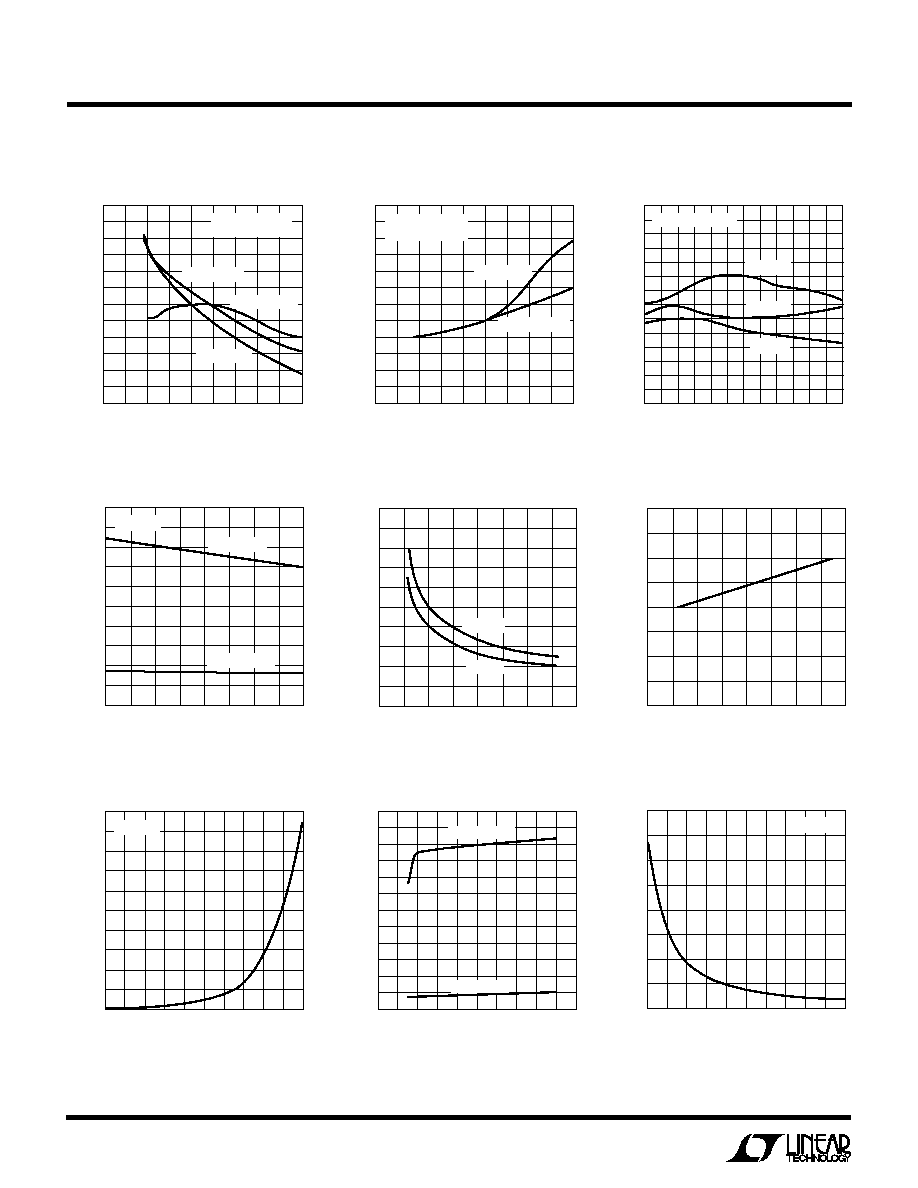
TYPICAL PERFOR
M
A
N
CE CHARACTERISTICS
U
W
Current Trip Threshold vs
Temperature
Switch Resistance vs
Input Voltage
Supply Current in Shutdown
TEMPERATURE (
°
C)
0
CURRENT TRIP THRESHOLD (mA)
80
1474/75 G04
20
40
60
500
400
300
200
100
0
V
IN
= 10V
R
SENSE
= 0
R
SENSE
= 1.1
INPUT VOLTAGE (V)
0
R
DS(ON)
(
)
20
1474/75 G05
5
10
15
5
4
3
2
1
0
T = 70
°
C
T = 25
°
C
INPUT VOLTAGE (V)
0
SUPPLY CURRENT (
µ
A)
20
1474/75 G06
5
10
15
10.0
7.5
5.0
2.5
0
Switch Leakage Current vs
Temperature
V
IN
DC Supply Current
Off-Time vs Output Voltage
% OF REGULATED OUTPUT VOLTAGE (%)
0
OFF-TIME (
µ
s)
100
1474/75 G09
20
40
60
80
80
60
40
20
0
V
IN
= 10V
INPUT VOLTAGE (V)
0
SUPPLY CURRENT (
µ
A)
4
8
16
20
1474/75 G08
12
120
100
80
60
40
20
0
ACTIVE MODE
SLEEP MODE
TEMPERATURE (
°
C)
0
LEAKAGE CURRENT (
µ
A)
1474/75 G07
40
60
80
100
1.0
0.8
0.6
0.4
0.2
0
20
V
IN
= 18V
Efficiency vs Input Voltage
Line Regulation
Load Regulation
INPUT VOLTAGE (V)
0
EFFICIENCY (%)
4
8
16
1474/75 G01
12
100
95
90
85
80
75
70
I
LOAD
= 25mA
I
LOAD
= 200mA
FIGURE 1 CIRCUIT
L: CDRH73-101
I
LOAD
= 1mA
INPUT VOLTAGE (V)
0
V
OUT
(mV)
4
8
16
1474/75 G02
12
40
30
20
10
0
10
20
FIGURE 1 CIRCUIT
I
LOAD
= 100mA
R
SENSE
= 0.33
R
SENSE
= 0
LOAD CURRENT (mA)
0
V
OUT
(mV)
40
30
20
10
0
10
20
30
1474/75 G03
100
250
50
150
200
300
FIGURE 1 CIRCUIT
V
IN
= 15V
V
IN
= 10V
V
IN
= 5V
5
LTC1474/LTC1475
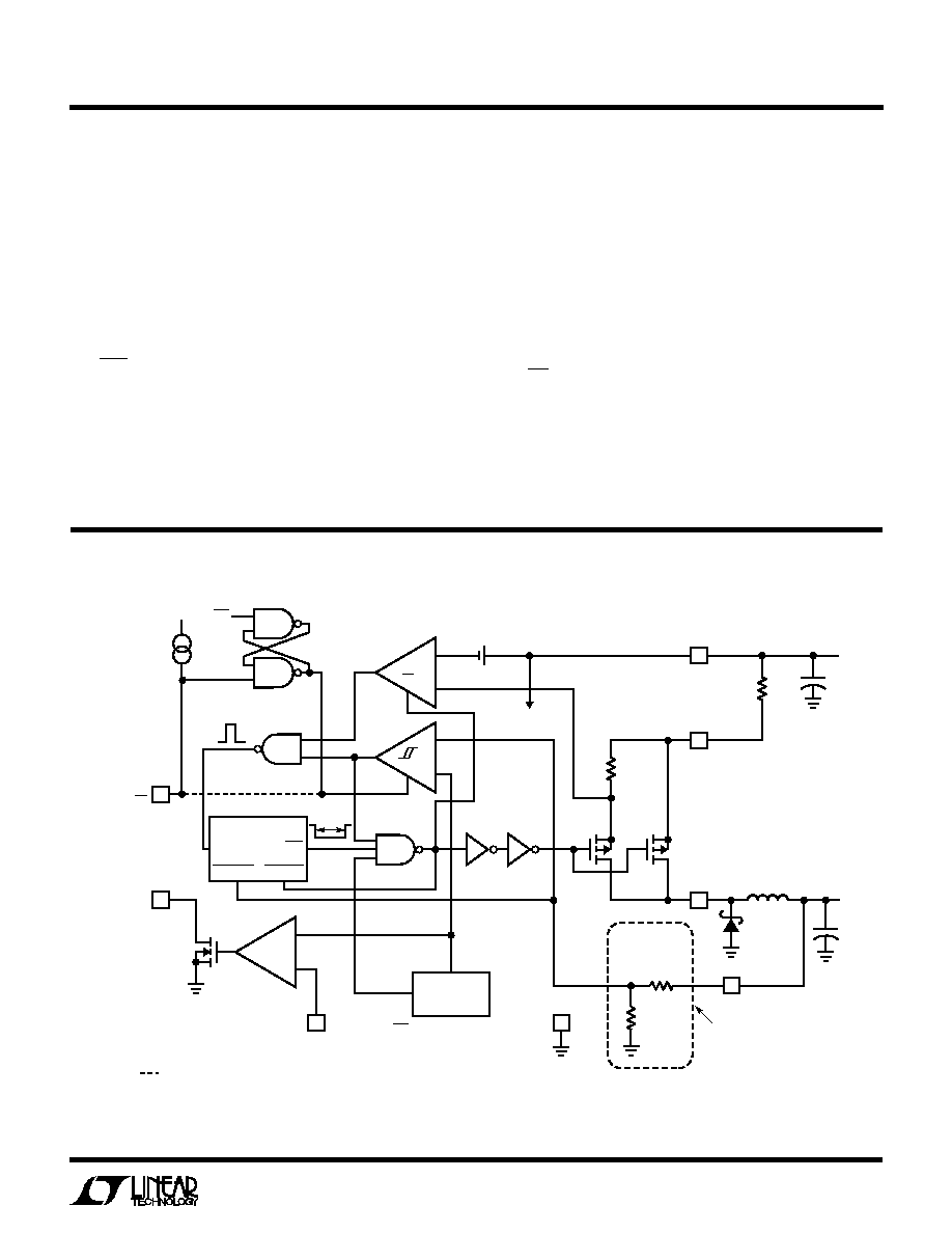
FU
N
CTIO
N
AL DIAGRA
U
U
W
LTC1474: LBI
LTC1475: LBI/OFF
+
+
+
×
1
µ
A
LBI/OFF
LBO
4.75
µ
s
1-SHOT
1.23V
REFERENCE
GND
1474/75 FD
4
2
8
1.23V
1M
3M
(5V VERSION)
1.68M
(3.3V VERSION)
READY
STRETCH
V
CC
V
IN
V
IN
V
OUT
V
OUT
/V
FB
1
×
C
ON
V
LB
ON
5
SW
SENSE
R
SENSE
(OPTIONAL)
20
×
100mV
WAKEUP
TRIGGER
OUT
LTC1474: RUN
LTC1475: ON
1
5
6
7
+
+
×
CONNECTION NOT PRESENT IN LTC1474 SERIES
CONNECTION PRESENT IN LTC1474 SERIES ONLY
3
OUTPUT DIVIDER IS
IMPLEMENTED EXTERNALLY IN
ADJUSTABLE VERSIONS
PI
N
FU
N
CTIO
N
S
U
U
U
V
OUT
/V
FB
(Pin 1): Feedback of Output Voltage. In the fixed
versions, an internal resistive divider divides the output
voltage down for comparison to the internal 1.23V refer-
ence. In the adjustable versions, this divider must be
implemented externally.
LBO (Pin 2): Open Drain Output of the Low Battery
Comparator. This pin will sink current when Pin 3 is below
1.23V.
LBI/OFF (Pin 3): Input to Low Battery Comparator. This
input is compared to the internal 1.23V reference. For the
LTC1475, a momentary ground on this pin puts regulator
in shutdown mode.
GND (Pin 4): Ground Pin.
SW (Pin 5): Drain of Internal PMOS Power Switch. Cath-
ode of Schottky diode must be closely connected to this
pin.
SENSE (Pin 6): Current Sense Input for Monitoring Switch
Current and Source of Internal PMOS Power Switch.
Maximum switch current is programmed with a resistor
between SENSE and V
IN
pins.
V
IN
(Pin 7): Main Supply Pin.
RUN/ON (Pin 8): On LTC1474, voltage level on this pin
controls shutdown/run mode (ground = shutdown, open/
high = run). On LTC1475, a momentary ground on this pin
puts regulator in run mode. A 100k series resistor must be
used between Pin 8 and the switch or control voltage.