 | ÐлекÑÑоннÑй компоненÑ: LTC1479IG | СкаÑаÑÑ:  PDF PDF  ZIP ZIP |
Äîêóìåíòàöèÿ è îïèñàíèÿ www.docs.chipfind.ru
1
LTC1479
PowerPath Controller
for Dual Battery Systems
FEATURES
DESCRIPTIO
N
U
s
Complete Power Path Management for Two
Batteries, DC Power Source, Charger and Backup
s
Compatible with Li-Ion, NiCd, NiMH and Lead-Acid
Battery Chemistries
s
"3-Diode" Mode Ensures Powers is Available
under "Cold Start" Conditions
s
All N-Channel Switching Reduces Power Losses
s
Capacitor and Battery Inrush Current Limited
s
"Seamless" Switching Between Power Sources
s
Independent Charging and Monitoring of Two
Battery Packs
s
New, Small Footprint, 36-Lead SSOP Package
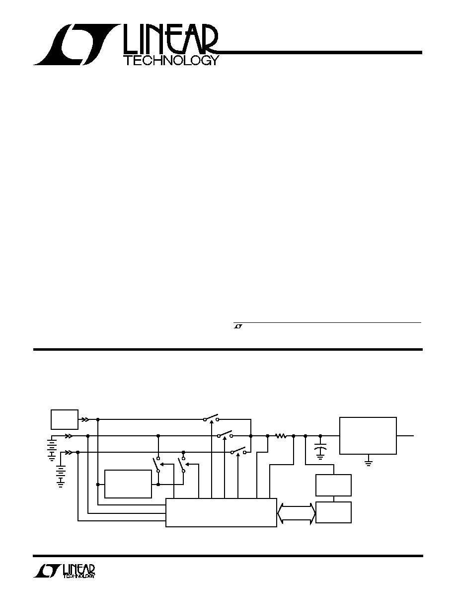
The LTC
®
1479 is the "heart" of a total power management
solution for single and dual battery notebook computers
and other portable equipment. The LTC1479 directs power
from up to two battery packs and a DC power source to the
input of the main system switching regulator. It works in
concert with related LTC power management products
(e.g. LTC1435, LT
®
1511, etc.) to create a total system
solution; starting from the batteries and the DC power
source, and ending at the input of each of the computer's
complex loads. A system-provided power management
µ
P monitors and actively directs the LTC1479.
The LTC1479 uses low loss N-channel MOSFET switches
to direct power from three main sources. An adaptive
current limiting scheme reduces capacitor and battery
inrush current by controlling the gates of the MOSFET
switches during transitions. The LTC1479 interfaces di-
rectly to the LT1510, LT1511 and LT1620/LTC1435 bat-
tery charging circuits.
TYPICAL APPLICATIO
N
U
Dual Battery PowerPath
TM
Controller System Block Diagram
PowerPath is a trademark of Linear Technology Corporation.
, LTC and LT are registered trademarks of Linear Technology Corporation.
s
Notebook Computer Power Management
s
Portable Instruments
s
Handheld Terminals
s
Portable Medical Equipment
s
Portable Industrial Control Equipment
APPLICATIO
N
S
U
BAT1
BAT2
BATTERY CHARGER
(LT1510/LT1511/
LT1620/LTC1435)
SW A/B
R
SENSE
SW C/D
SW E/F
SW G
SW H
+
C
IN
DCIN
1479 TA01
5V
AC
ADAPTER
POWER
MANAGEMENT
µ
P
BACKUP
REGULATOR
(LT1304)
HIGH EFFICIENCY
DC/DC SWITCHING
REGULATOR
(LTC1435/LTC1438
ETC.)
LTC1479
PowerPath CONTROLLER
STATUS &
CONTROL
2
LTC1479
ABSOLUTE
M
AXI
M
U
M
RATINGS
W
W
W
U
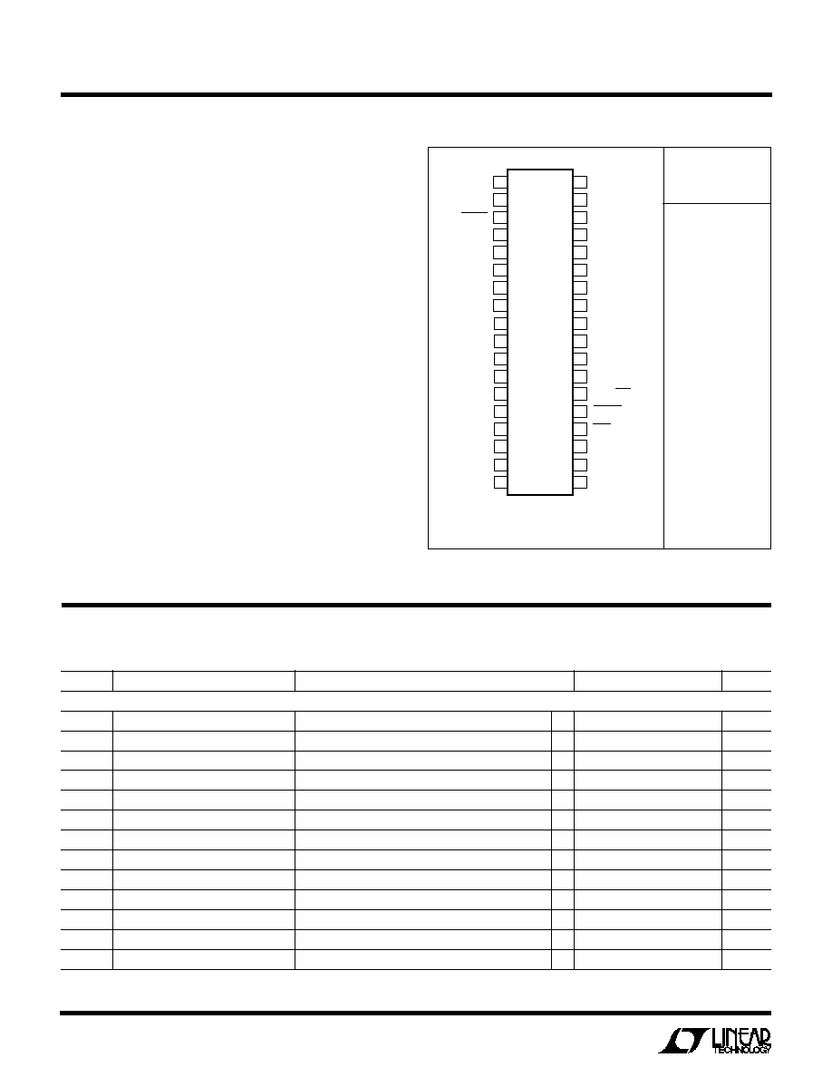
PACKAGE/ORDER I
N
FOR
M
ATIO
N
W
U
U
ORDER PART
NUMBER
T
JMAX
= 100
°
C,
JA
= 95
°
C/ W
Consult factory for Military grade parts.
1
2
3
4
5
6
7
8
9
10
11
12
13
14
15
16
17
18
TOP VIEW
G PACKAGE (209 mils)
36-LEAD PLASTIC SSOP
36
35
34
33
32
31
30
29
28
27
26
25
24
23
22
21
20
19
DCIN
DCDIV
LOBAT
GA
SAB
GB
GC
SCD
GD
GE
SEF
GF
SENSE
+
SENSE
V
CC
V
GG
V
+
SW
V
BKUP
BAT1
BAT2
BDIV
V
BAT
CHGMON
BATSEL
GG
SG
GH
SH
DCINGOOD
DCIN/BAT
BATDIS
3DM
CHGSEL
V
CCP
GND
DCIN, BAT1, BAT2 Supply Voltages .......... 0.3V to 32V
SENSE
+
, SENSE
, V
BAT
, V
+
..................... 0.3V to 32V
GA, GB, GC, GD, GE, GF, GG, GH .............. 0.3V to 42V
SAB, SCD, SEF, SG, SH ............................ 0.3V to 32V
SW, V
GG
................................................... 0.3V to 42V
DCDIV, BDIV ............................................ 0.3V to 5.5V
All Logic Inputs (Note 1).......................... 0.3V to 7.5V
All Logic Outputs (Note 1) ....................... 0.3V to 7.5V
V
CC
Regulator Output Current ................................ 1mA
V
CCP
Regulator Output Current .............................. 1mA
V
+
Output Current .................................................. 1mA
V
GG
Regulator Output Current ............................ 100
µ
A
Operating Temperature
LTC1479CG ............................................. 0
°
C to 70
°
C
LTC1479IG ........................................ 40
°
C to 85
°
C
Junction Temperature ........................................... 125
°
C
Storage Temperature Range ................. 65
°
C to 150
°
C
Lead Temperature (Soldering, 10 sec).................. 300
°
C
SYMBOL
PARAMETER
CONDITIONS
MIN
TYP
MAX
UNITS
Power Supplies
V
DCIN
DCIN Operating Range
(Mode 1) DCIN Selected
6
28
V
V
BAT1
Battery 1 Operating Range
(Mode 5) Battery 1 Selected
6
28
V
V
BAT2
Battery 2 Operating Range
(Mode 6) Battery 2 Selected
6
28
V
V
BKUP
Backup Operating Range
(Mode 8) Backup Operation
6
28
V
I
DCIN
DCIN Operating Current
(Mode 1) DCIN Selected
175
500
µ
A
I
VBAT1
Battery 1 Operating Current
(Mode 5) Battery 1 Selected
150
500
µ
A
I
VBAT2
Battery 2 Operating Current
(Mode 6) Battery 2 Selected
150
500
µ
A
I
VBKUP
Backup Operating Current
(Mode 8) Backup Operation (V
BKUP
= 6V)
40
100
µ
A
V
CCP
V
CCP
Regulator Output Voltage
(Modes 1, 5, 6) DCIN, Battery 1 or Battery 2 Selected
q
4.0
4.8
6.0
V
V
CC
V
CC
Regulator Output Voltage
(Modes 1, 5, 6) DCIN, Battery 1 or Battery 2 Selected
q
3.3
3.6
3.9
V
V
GG
V
GG
Gate Supply Voltage
(Modes 1, 5, 6) DCIN, Battery 1 or Battery 2 Selected
q
34.0
36.3
40.0
V
V
UVLO
UV Lockout Threshold
(Mode 9) No Power, V
BATX
Falling from 12V
4.0
4.5
5.0
V
V
UVLOHYS
UV Lockout Hysteresis
(Mode 9) No Power, V
BATX
Rising from 1V
0.2
0.5
1.0
V
V
DCIN
= 25V, V
BAT1
= 16V, V
BAT2
= 12V, T
A
= 25
°
C unless otherwise noted. (Note 2)
DC ELECTRICAL CHARACTERISTICS
LTC1479CG
LTC1479IG
3
LTC1479
V
DCIN
= 25V, V
BAT1
= 16V, V
BAT2
= 12V, T
A
= 25
°
C unless otherwise noted. (Note 2)
DC ELECTRICAL CHARACTERISTICS
SYMBOL
PARAMETER
CONDITIONS
MIN
TYP
MAX
UNITS
DCIN Good Monitor
V
THDCDIV
DCDIV Threshold Voltage
(Mode 1) V
DCDIV
Rising from 1V to 1.5V
q
1.190
1.215
1.240
V
V
HYSDCDIV
DCDIV Hysteresis Voltage
(Mode 1) V
DCDIV
Falling from 1.5V to 1V
10
35
50
mV
I
BIASDCDIV
DCDIV Input Bias Current
(Mode 1) V
DCDIV
= 1.5V
20
nA
V
LODCGD
DCINGOOD Output Low Voltage
(Mode 1) V
DCDIV
= 1V, I
DCINGOOD
= 100
µ
A
0
0.1
0.4
V
I
PUDCGD
DCINGOOD Pull-Up Current
(Mode 1) V
DCDIV
= 1.5V, V
DCINGOOD
= 0V
1
2
6
µ
A
I
LKGDCGD
DCINGOOD Leakage Current
(Mode 1) V
DCDIV
= 1.5V, V
DCINGOOD
= 7V
±
1
µ
A
Battery Monitor
V
THLOBAT
Low-Battery Threshold Voltage
(Modes 5, 6) V
BDIV
Falling from 1.5V to 1V
q
1.190
1.215
1.240
V
V
HYSLOBAT
Low-Battery Hysteresis Voltage
(Modes 5, 6) V
BDIV
Rising from 1V to 1.5V
10
35
50
mV
I
BIASBDIV
BDIV Input Bias Current
(Modes 5, 6) V
BDIV
= 1.5V
20
nA
V
LOLOBAT
LOBAT Output Low Voltage
(Modes 5, 6) V
BDIV
= 1V, I
LOBAT
= 100
µ
A
0
0.1
0.4
V
I
LKGLOBAT
LOBAT Output Leakage Current
(Modes 5, 6) V
BDIV
= 1.5V, V
LOBAT
= 7V
±
1
µ
A
R
ONBATSW
Battery Switch ON Resistance
(Modes 5, 6) Each Switch Tested Independently
200
400
800
I
LKGBATSW
Battery Switch OFF Leakage
(Modes 5, 6) Each Switch Tested Independently
±
1
µ
A
Gate Drivers
V
GS(ON)
Gate-to-Source ON Voltage (GA to GF) (Modes 1, 2, 4, 5, 6) I
GS
= 1
µ
A
5.0
5.5
7.0
V
Gate-to-Source ON Voltage (GG, GH)
(Modes 2, 4) I
GS
= 1
µ
A
4.5
5.2
7.0
V
V
GS(OFF)
Gate-to-Source OFF Voltage
(Modes 1, 2, 4, 5, 6) I
GS
= 100
µ
A
0
0.4
V
I
BSENSE
+
SENSE
+
Input Bias Current
(Modes 1, 5, 6)
5
15
30
µ
A
I
BSENSE
SENSE
Input Bias Current
(Modes 1, 5, 6)
5
15
30
µ
A
V
SENSE
Inrush Current Limit Sense Voltage
(Modes 1, 5, 6)
q
0.15
0.20
0.25
V
I
PDSAB
SAB Pull-Down Current
(Modes 5, 6) V
SAB
= 10V
30
100
300
µ
A
I
PDSCD
SCD Pull-Down Current
(Mode 1) V
SCD
= 10V
30
100
300
µ
A
I
PDSEF
SEF Pull-Down Current
(Mode 1) V
SEF
= 10V
30
100
300
µ
A
I
PDSG
SG Pull-Down Current
(Mode 1) V
SG
= 10V
3
mA
I
PDSH
SH Pull-Down Current
(Mode 1) V
SH
= 10V
3
mA
Charge Monitor
R
ONCMON
CHGMON Switch ON Resistance
(Modes 5, 6) Each Switch Tested Independently
50
150
250
I
LKGCMON
CHGMON Switch OFF Leakage
(Modes 5, 6) Each Switch Tested Independently
±
1
µ
A
Digital Inputs
V
HIDIGIN
Input High Voltage
(Mode 1) All Digital Inputs
q
2
V
V
LODIGIN
Input Low Voltage
(Mode 1) All Digital Inputs
q
0.8
V
I
HIDIGIN
Input Leakage Current
(Mode 1) All Digital Inputs, V
DIGINX
= 7V
±
1
µ
A
I
LODIGIN
Input Leakage Current
(Mode 1) V
DIGINX
= 0V (Note 3)
±
1
µ
A
I
PUDIGIN
Input Pull-Up Current
(Mode 1) V
DIGINX
= 0V (Note 4)
1
2
6
µ
A
4
LTC1479
AC ELECTRICAL CHARACTERISTICS
V
DCIN
= 25V, V
BAT1
= 16V, V
BAT2
= 12V, T
A
= 25
°
C unless otherwise noted. (Note 2)
SYMBOL
PARAMETER
CONDITIONS
MIN
TYP
MAX
UNITS
t
ONGA/GB
Gate A/B Turn-On Time
V
GS
> 3V (Note 5)
30
µ
s
t
ONGC/GD
Gate C/D Turn-On Time
V
GS
> 3V (Note 5)
30
µ
s
t
ONGE/GF
Gate E/F Turn-On Time
V
GS
> 3V (Note 5)
30
µ
s
t
OFFGA/GB
Gate A/B Turn-Off Time
V
GS
< 1V (Note 5)
3
µ
s
t
OFFGC/GD
Gate C/D Turn-Off Time
V
GS
< 1V (Note 5)
3
µ
s
t
OFFGE/GF
Gate E/F Turn-Off Time
V
GS
< 1V (Note 5)
3
µ
s
t
ONGG/GH
Gate G/H Turn-On Time
V
GS
> 3V (Note 5)
300
µ
s
t
OFFGG/GH
Gate G/H Turn-Off Time
V
GS
< 1V (Note 5)
5
µ
s
f
OVGG
V
GG
Reg Operating Frequency
30
kHz
t
dLOBAT
LOBAT Delay Times
V
BDIV
=
±
100mV, R
PULLUP
= 51k
5
µ
s
t
dDCINGOOD
DCINGOOD Delay Times
V
DCDIV
=
±
100mV, R
PULLUP
= 51k
5
µ
s
The
q
denotes specifications which apply over the full operating
temperature range.
Note 1: The logic inputs are high impedance CMOS gates with ESD
protection diodes to ground and therefore should not be forced below
ground. These inputs can however be driven above the V
CCP
or V
CC
supply
rails as there are no clamping diodes connected between the input pins
and the supply rails. This facilitates operation in mixed 5V/3V systems.
Note 2: The Selected Operating Mode Truth Table, which defines the
operating conditions and logical states associated with each "normal"
operating mode, should be used in conjunction with the Electrical
Characteristics table to establish test conditions. Actual production test
conditions may be more stringent.
Note 3: The following inputs are high impedance CMOS inputs:
3DM and DCIN/BAT and have no internal pull-up current.
Note 4: The following inputs have built-in 2
µ
A pull-up current sources
(passed through series diodes): BATSEL, BATDIS and CHGSEL.
Note 5: Gate turn-on and turn-off times are measured with no inrush
current limiting, i. e., V
SENSE
= 0V, using Si4936DY MOSFETs in the typical
application circuit.
TRUTH TABLE
SELECTED MODES
LOGIC INPUTS
SWITCH STATUS
OUTPUTS
SW
SW
SW
SW
SW
NO. MODE
3DM DCIN/BAT BATSEL
BATDIS
CHGSEL
A/B
C/D
E/F
G
H
CHGMON
V
BAT
LOBAT
DCINGOOD
1
DC Operation
H
H
H
L
H
On
Off
Off
Off
Off
Hi-Z
BAT1
H
H
2
DC Operation and
H
H
H
H
H
On
Off
Off
On
Off
BAT1
BAT1
H
H
BAT1 Charging
3
DC Operation and
H
H
L
L
L
On
Off
Off
Off
Off
Hi-Z
BAT2
H
H
BAT2 Disconnected
4
DC Operation and
H
H
L
H
L
On
Off
Off
Off
On
BAT2
BAT2
H
H
BAT2 Charging
5
BAT1 Operation
H
L
H
H
H
Off
On
Off
Off
Off
Hi-Z
BAT1
H
L
6
BAT2 Operation
H
L
L
H
H
Off
Off
On
Off
Off
Hi-Z
BAT2
H
L
7
BAT1 Low and
H
L
H
L
H
Off
Off
Off
Off
Off
Hi-Z
BAT1
L
L
Disconnected
8
Backup Operation
H
L
H
L
H
Off
Off
Off
Off
Off
Hi-Z
BAT1
L
L
9
No Power
L
L
L
L
L
Off
Off
Off
Off
Off
Hi-Z
BAT2
L
L
(No Backup)
10 DC Reconnected
L
L
H
L
H
3DM* 3DM* 3DM* Off
Off
Hi-Z
BAT1
L
H
11 DC Connected
H
H
H
L
H
On
Off
Off
Off
Off
Hi-Z
BAT1
L
H
and Reset
(Selected Operating Modes)
* 3DM = Three Diode Mode. When this mode is invoked, only the first
MOSFET switch in each back-to-back switch pair, i. e., SW A, SW C and
SW E is turned on. Current may still pass through the inherent body
diode of the idled switches, i.e., SW B, SW D and SW F to help restart
the system after abnormal operating conditions have been encountered.
See the Timing Diagram and Applications Information sections for
further details.
5
LTC1479
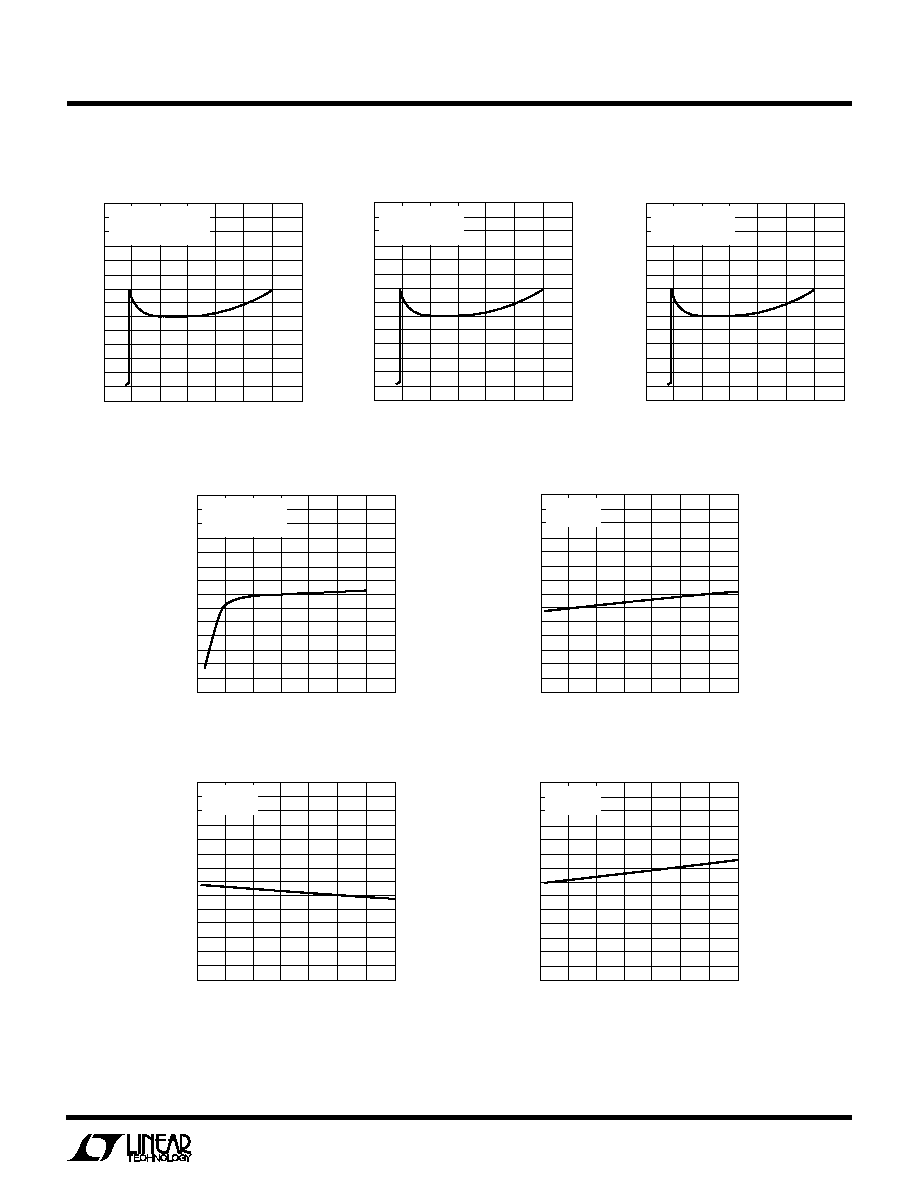
TYPICAL PERFOR
M
A
N
CE CHARACTERISTICS
U
W
DCIN Supply Current
BAT1 Supply Current
BAT2 Supply Current
V
GG
Supply Voltage
JUNCTION TEMPERATURE (
°
C)
50
38
40
44
25
75
1479 G05
36
34
25
0
50
100
125
32
30
42
V
GG
SUPPLY VOLTAGE (V)
MODE 1
V
DCIN
= 24V
V
BKUP
Supply Current
V
BKUP
SUPPLY VOLTAGE (V)
0
40
50
70
15
25
1479 G04
30
20
5
10
20
30
35
10
0
60
V
BKUP
SUPPLY CURRENT (
µ
A)
MODE 8
NO OTHER POWER
T
J
= 25
°
C
V
CC
Supply Voltage
JUNCTION TEMPERATURE (
°
C)
50
3.7
3.8
4.0
25
75
1479 G06
3.6
3.5
25
0
50
100
125
3.4
3.3
3.9
V
CC
SUPPLY VOLTAGE (V)
MODE 1
V
DCIN
= 24V
V
CCP
Supply Voltage
JUNCTION TEMPERATURE (
°
C)
50
5.0
5.5
6.5
25
75
1479 G07
4.5
4.0
25
0
50
100
125
3.5
3.0
6.0
V
CCP
SUPPLY VOLTAGE (V)
MODE 1
V
DCIN
= 24V
DCIN SUPPLY VOLTAGE (V)
0
200
250
350
15
25
1479 G01
150
100
5
10
20
30
35
50
0
300
DCIN SUPPLY CURRENT (
µ
A)
MODE 1, DCDIV = 1.5V
NO OTHER POWER
T
J
= 25
°
C
BAT1 SUPPLY VOLTAGE (V)
0
200
250
350
15
25
1479 G02
150
100
5
10
20
30
35
50
0
300
BAT1 SUPPLY CURRENT (
µ
A)
MODE 5
NO OTHER POWER
T
J
= 25
°
C
BAT2 SUPPLY VOLTAGE (V)
0
200
250
350
15
25
1479 G03
150
100
5
10
20
30
35
50
0
300
BAT2 SUPPLY CURRENT (
µ
A)
MODE 6
NO OTHER POWER
T
J
= 25
°
C