Äîêóìåíòàöèÿ è îïèñàíèÿ www.docs.chipfind.ru
1
LTC1502-3.3
Single Cell to 3.3V
Regulated Charge Pump
DC/DC Converter
s
Input Voltage Range: 0.9V to 1.8V
s
0.9V Guaranteed Start-Up Voltage
s
Regulated Output Voltage: 3.3V
±
4%
s
Output Current: 10mA (V
IN
1V)
s
No Inductors
s
Shutdown Disconnects Load from V
IN
s
Low Operating Current: 40
µ
A
s
Low Shutdown Current: 5
µ
A
s
Short-Circuit and Overtemperature Protected
s
Application Circuit Fits in < 0.125in
2
PCB Area
s
Available in 8-Pin MSOP and SO Packages
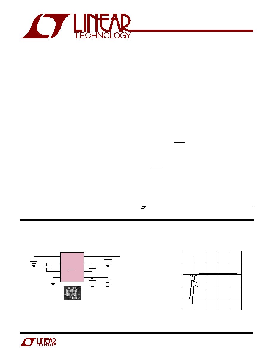
The LTC
®
1502-3.3 is a quadrupler charge pump DC/DC
converter that produces a regulated 3.3V output from a
single alkaline cell input. It requires only five small external
capacitors--no inductors are required. Low supply cur-
rent (40
µ
A typical, 5
µ
A in shutdown) and minimal external
components make the LTC1502-3.3 ideal for space and
power conscious single-cell applications. The total printed
circuit board area of the circuit shown below is less than
0.125in
2
.
Forcing the C1
/SHDN pin low through an external resis-
tive pull-down puts the part into shutdown mode. During
shutdown, the internal oscillator is stopped and the load is
disconnected from V
IN
. An internal pull-up current on the
C1
/SHDN pin forces the part back into normal operation
once the pull-down resistance is removed.
The LTC1502-3.3 is short-circuit protected and survives
an indefinite V
OUT
short to ground. The LTC1502-3.3 is
available in 8-pin MSOP and SO packages.
, LTC and LT are registered trademarks of Linear Technology Corporation.
Output Voltage vs Input Voltage
1
2
3
1502-3.3 TA01
4
8
7
1
µ
F
6
5
V
IN
GND
1
µ
F
V
IN
SINGLE CELL
NiCd or
ALKALINE
10
µ
F
10
µ
F
10
µ
F
V
OUT
= 3.3V
I
OUT
= 10mA
LTC1502-3.3
C2
C1
+
C1
/SHDN
V
OUT
C3
+
C3
Single Cell to 3.3V DC/DC Converter
s
Pagers
s
Battery Backup Supplies
s
Portable Electronic Equipment
s
Handheld Medical Instruments
s
Glucose Meters
INPUT VOLTAGE (V)
0.8
OUTPUT VOLTAGE (V)
3.3
3.4
3.5
1.6
1502-3.3 TA02
3.2
3.1
3.0
1.0
1.2
1.4
1.8
T
A
= 25
°
C
I
OUT
= 10mA
I
OUT
= 15mA
FEATURES
DESCRIPTIO
U
APPLICATIO S
U
TYPICAL APPLICATIO
U
PCB LAYOUT FITS IN < 0.125IN
2
2
LTC1502-3.3
ABSOLUTE
M
AXI
M
U
M
RATINGS
W
W
W
U
Operating Temperature Range
Commercial ............................................ 0
°
C to 70
°
C
Extended Commercial (Note 4) .......... 40
°
C to 85
°
C
Industrial ........................................... 40
°
C to 85
°
C
Lead Temperature (Soldering, 10 sec)................. 300
°
C
V
IN
to GND .................................................. 0.3V to 2V
V
OUT
to GND ............................................... 0.3V to 5V
All Other Pins to GND ................................. 0.3V to 5V
V
OUT
Short-Circuit Duration ............................ Indefinite
Storage Temperature Range ................ 65
°
C to 150
°
C
(Note 1)
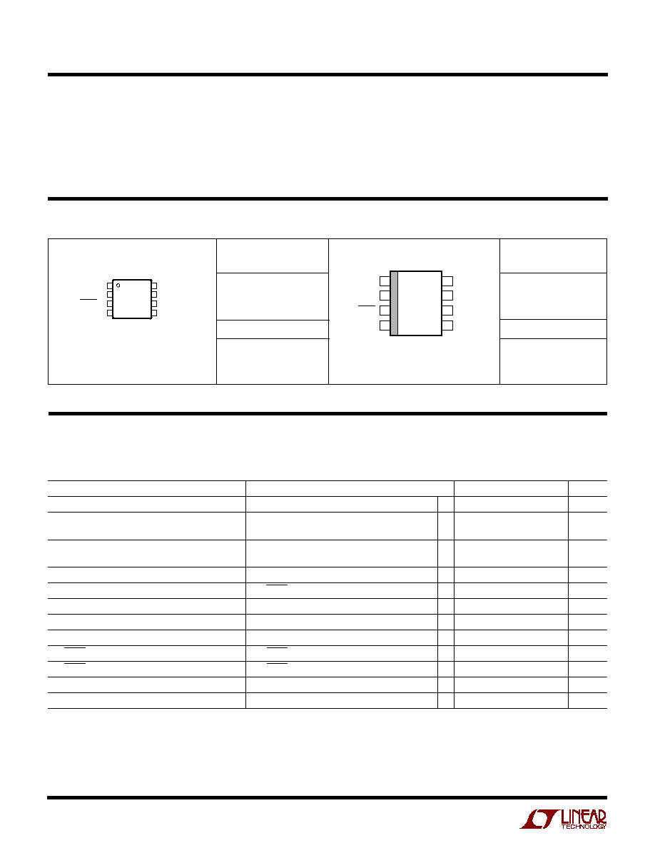
PACKAGE/ORDER I
N
FOR
M
ATIO
N
W
U
U
ORDER PART
NUMBER
ORDER PART
NUMBER
LTC1502CS8-3.3
LTC1502IS8-3.3
S8 PART MARKING
Consult factory for Military grade parts.
T
JMAX
= 125
°
C,
JA
= 150
°
C/ W
LTC1502CMS8-3.3
MS8 PART MARKING
LTEC
T
JMAX
= 125
°
C,
JA
= 250
°
C/ W
1
2
3
4
C2
C1
+
C1
/SHDN
GND
8
7
6
5
V
OUT
C3
+
C3
V
IN
TOP VIEW
MS8 PACKAGE
8-LEAD PLASTIC MSOP
1
2
3
4
8
7
6
5
TOP VIEW
V
OUT
C3
+
C3
V
IN
C2
C1
+
C1
/SHDN
GND
S8 PACKAGE
8-LEAD PLASTIC SO
150233
502I33
ELECTRICAL CHARACTERISTICS
PARAMETER
CONDITIONS
MIN
TYP
MAX
UNITS
V
IN
Operating Voltage
q
0.9
1.8
V
Minimum V
IN
Start-Up Voltage
T
A
= 0
°
C to 70
°
C (Note 2)
q
0.75
0.9
V
T
A
= 40
°
C to 85
°
C (Note 2)
q
1.1
V
V
OUT
Voltage
I
OUT
3.5mA, 0.9V
V
IN
1.8V
q
3.17
3.3
3.43
V
I
OUT
10mA, 1V
V
IN
1.8V
q
3.17
3.3
3.43
V
V
IN
Operating Current
I
OUT
= 0mA
q
40
90
µ
A
V
IN
Shutdown Current
C1
/SHDN = 0V
q
5
15
µ
A
Output Ripple
I
OUT
= 10mA, V
IN
= 1.25V
50
mV
P-P
Efficiency
V
IN
= 1V, I
OUT
= 10mA
77
%
Switching Frequency
Oscillator Free-Running
500
kHz
C1
/SHDN Shutdown Input Threshold
C1
/SHDN in Hi-Z Sampling State
q
0.20
0.55
0.85
V
C1
/SHDN Shutdown Input Current
C1
/SHDN = 0V (Note 3)
q
0.5
2.5
8
µ
A
V
OUT
Turn-On Time
V
IN
= 1V, I
OUT
= 0mA
5
ms
V
OUT
Short-Circuit Current
V
IN
= 1.5V, V
OUT
Forced to 0V
20
mA
The
q
denotes the specifications which apply over the full operating temperature range, otherwise specifications are at T
A
= 25
°
C.
V
IN
= 0.9V to 1.8V, C1 = C3 = 1
µ
F, C
IN
= C2 = C
OUT
= 10
µ
F unless otherwise specified.
Note 1: Absolute Maximum Ratings are those values beyond which the life
of the device may be impaired.
Note 2: Start-up testing is done with a 100k
equivalent load on V
OUT
.
Note 3: Currents flowing into the device are positive polarity. Currents
flowing out of the device are negative polarity.
Note 4: Commercial grade specifications are guaranteed over the 0
°
C to
70
°
C operating temperature range. In addition, commercial grade
specifications are assured over the 40
°
C to 85
°
C operating temperature
range by design, characterization and correlation with statistical process
controls. Industrial grade specifications are guaranteed and tested over the
40
°
C to 85
°
C operating temperature range.
3
LTC1502-3.3
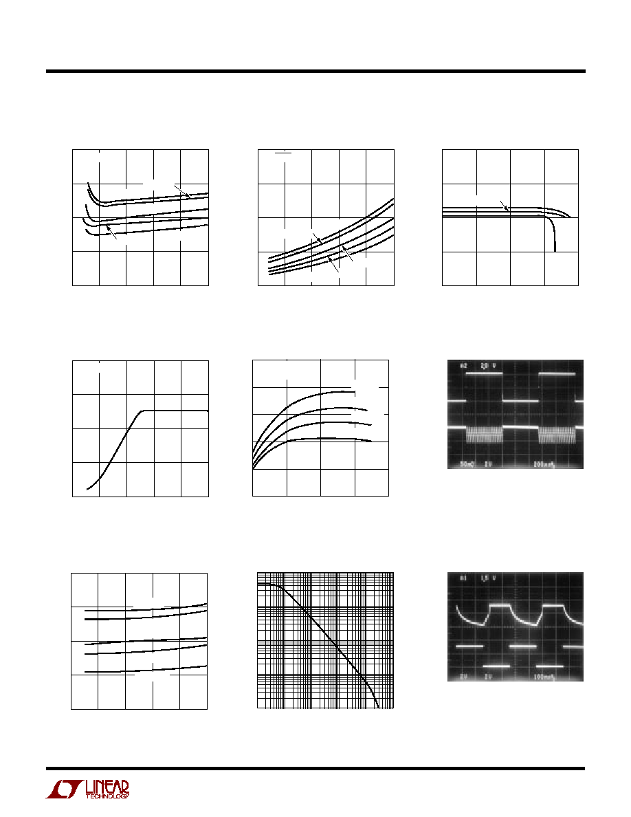
TYPICAL PERFOR A CE CHARACTERISTICS
U
W
INPUT VOLTAGE (V)
0.8
INPUT CURRENT (
µ
A)
40
60
1.6
1502-3.3 G01
20
0
1.0
1.2
1.4
1.8
80
T
A
= 25
°
C
T
A
= 0
°
C
T
A
= 40
°
C
I
OUT
= 0mA
T
A
= 70
°
C
T
A
= 85
°
C
No Load Input Current
vs Input Voltage
OUTPUT CURRENT (mA)
0.01
OUTPUT VOLTAGE (V)
3.30
3.35
T
A
= 25
°
C
V
IN
= 1V
100
1502-3.3 G03
3.25
3.20
0.1
1
10
3.40
V
IN
= 1.5V
V
IN
= 1.8V
Output Voltage vs Output Current
Shutdown Input Current
vs Input Voltage
INPUT VOLTAGE (V)
0.8
INPUT CURRENT (
µ
A)
8
12
1.6
1502-3.3 G02
4
0
1.0
1.2
1.4
1.8
16
T
A
= 70
°
C
T
A
= 85
°
C
T
A
= 25
°
C
T
A
= 40
°
C
T
A
= 0
°
C
C1
/SHDN = 0V
Maximum Start-Up Load Current
vs Input Voltage
INPUT VOLTAGE (V)
0.8
LOAD CURRENT (mA)
8
12
1.6
1502-3.3 G04
4
0
1.0
1.2
1.4
1.8
16
T
A
= 25
°
C
Load Transient Response
200
µ
s/DIV
I
OUT
0mA to 10mA
5mA/DIV
V
OUT
AC COUPLED
50mV/DIV
Efficiency vs Output Current
OUTPUT CURRENT (mA)
0.01
EFFICIENCY (%)
40
60
100
1502-3.3 G05
20
0
0.1
1
10
100
80
T
A
= 25
°
C
V
OUT
= 3.3V
V
IN
= 1V
V
IN
= 1.25V
V
IN
= 1.5V
V
IN
= 1.8V
1502-3.3 G06
Oscillator Frequency
vs Input Voltage
Shutdown Waveforms
(See Figure 1)
Calculated Battery Life,
Battery = 2400mA · Hr AA Cell
INPUT VOLTAGE (V)
0.8
OSCILLATOR FREQUENCY (kHz)
500
600
1.6
1502-3.3 G07
400
300
1.0
1.2
1.4
1.8
700
T
A
= 70
°
C
T
A
= 40
°
C
T
A
= 25
°
C
T
A
= 85
°
C
T
A
= 0
°
C
AVERAGE LOAD CURRENT (mA)
0.001
10
BATTERY LIFE (HOURS)
1k
100k
0.1
1
10
0.01
100
1502-3.3 G08
100
10k
100
µ
s/DIV
V
OUT
2V/DIV
OFF
1502-3.3 G09
ON
V
IN
= 1.25V
R
LOAD
= 10k
T
A
= 25
°
C
V
CTRL
V
IN
= 1.25V
T
A
= 25
°
C
4
LTC1502-3.3
GND (Pin 4): Ground. Connect to a ground plane for best
performance.
V
IN
(Pin 5): Input Supply Voltage. Bypass V
IN
with a
10
µ
F
low ESR capacitor to ground.
C3
(Pin 6): Charge Pump 2 (CP2) Flying Capacitor
Negative Terminal.
C3
+
(Pin 7): Charge Pump 2 Flying Capacitor Positive
Terminal.
V
OUT
(Pin 8): 3.3V Regulated Output Voltage. V
OUT
is
disconnected from V
IN
during shutdown. Bypass V
OUT
with a
10
µ
F low ESR capacitor to ground.
PI
N
FU
N
CTIO
N
S
U
U
U
C2 (Pin 1): Charge Pump 1 (CP1) Output. This pin also
serves as the input supply for charge pump 2 (CP2). To
ensure proper start-up, the C2 pin must not be externally
loaded. Bypass the C2 pin with a
10
µ
F low ESR capacitor
to ground.
C1
+
(Pin 2): Charge Pump 1 Flying Capacitor Positive
Terminal.
C1
/SHDN (Pin 3): Charge Pump 1 Flying Capacitor Nega-
tive Terminal and Shutdown Input. Pulling this pin to
ground through a
100
resistor will put the part into
shutdown mode. With a high resistance pull-down FET,
the series resistor may be eliminated. The external pull-
down device must be high impedance for normal opera-
tion (see Applications Information). Peak voltage present
on this pin is approximately equal to V
IN
.
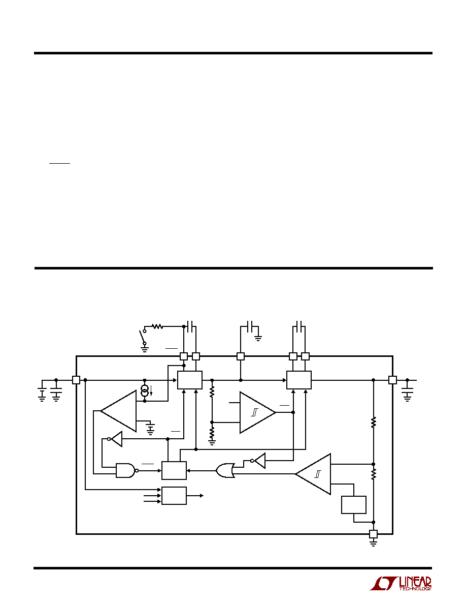
BLOCK DIAGRA
M
W
+
+
+
TIMING
CONTROL
BIAS
CONTROL
1.2V
REF
CP2
C3
C1
CP1
SHDN
OSCEN
INTERNAL
V
CC
CLK1/CLK2
U3
U4
U2
C2
V
OUT
HIZ2
HIZ1
1M
1.2M
2.1M
C
OUT
C2
COMP2
COMP3
COMP1
400k
0.55V
+
2.5
µ
A
C1
/SHDN
SHUTDOWN
C1
+
C3
C3
+
V
IN
3
2
C2
1
6
7
V
OUT
8
V
IN
5
GND
1502-3.3 BD
4
C
IN
5
LTC1502-3.3
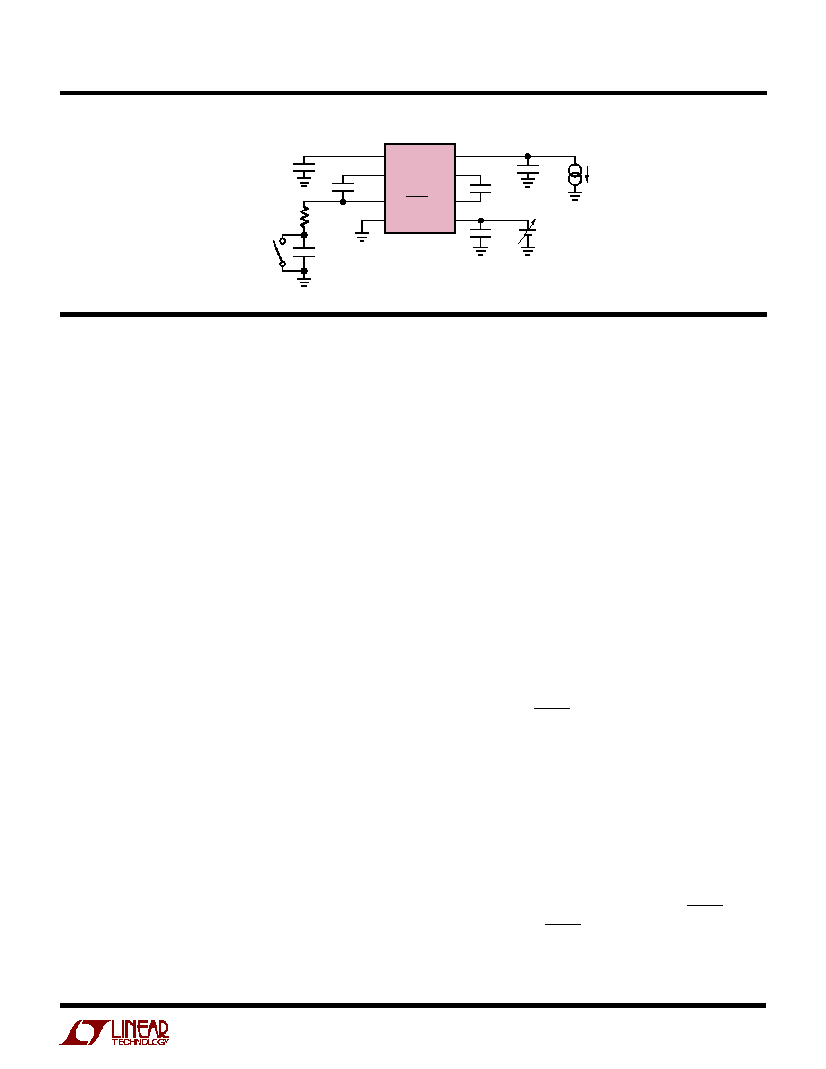
TEST CIRCUIT
APPLICATIO
N
S I
N
FOR
M
ATIO
N
W
U
U
U
Regulator Operation
The LTC1502-3.3 uses a quadrupler charge pump DC/DC
converter to produce a boosted output voltage. The
quadrupler charge pump consists of two voltage doubler
charge pumps (CP1 and CP2 on the Block Diagram)
cascaded in series. CP1 doubles the input voltage V
IN
and
the CP1 output voltage is stored on external capacitor C2.
The C2 pin also serves as the input for doubler CP2 whose
output is stored on the output capacitor C
OUT
. Each
doubler is controlled by a two-phase clock which is
generated in the Timing Control circuit. On phase one of
the clock, the flying capacitors C1 and C3 are charged to
their respective input voltages. On phase two each charged
flying capacitor is stacked on top of the input voltage and
discharged through an internal switch onto its respective
output. This sequence of charging and discharging the
CP1 and CP2 flying capacitors continues at the free
running oscillator frequency (500kHz typ) until the output
is in regulation.
Regulation is achieved by comparing the divided down
output voltage to a fixed voltage reference. The charge
pump clocks are disabled when the output voltage is
above the desired regulation point set by COMP1. When
the output has dropped below the lower trip point of
COMP1, the charge pump clocks are turned back on until
V
OUT
is boosted back into regulation.
Enhanced Start-Up
Enhanced start-up capability is provided by the COMP2
circuitry. COMP2 compares the divided down C2 voltage
to the input voltage V
IN
. The COMP2 output disables the
output charge pump CP2 whenever the divided C2 voltage
is lower than V
IN
. The CP2 output is thereby forced into a
high impedance state until the voltage on C2 has been
raised above V
IN
(the C2 pin should not be loaded for
proper start-up). This allows a higher internal gate drive
voltage to be generated (from the C2 pin) before the output
(V
OUT
) is connected to a load. Hysteresis in COMP2 forces
CP2 to be turned ON and OFF while C
OUT
is charging up to
prevent a lockup condition if C2 droops too low during
start-up. By the time the output nears the regulation point,
the C2 voltage is well above the lower trip point of COMP2
and CP2 will remain enabled. This method of disabling the
output charge pump while an internal boosted gate drive
supply is developed allows the part to start up at low
voltages with a larger output current load than would
otherwise be possible.
Shutdown
Shutdown is implemented using an external pull-down
device on the C1
/SHDN pin. The recommended external
pull-down device is an open-drain FET with resistive cur-
rent limiting (see Figure 1). The pull-down device must sink
up to 300
µ
A and pull down below 0.2V to ensure proper
shutdown operation, however, the actual series resistance
is not critical. The pull-down device must also go into a Hi-
Z state for the LTC1502-3.3 to become active.
The timing control circuitry forces the CP1 switches into
a high impedance state every 16 clock cycles. The Hi-Z
duration is equal to one clock cycle. At the end of the
Hi-Z time interval, the voltage on the C1
/SHDN pin is
sampled. If the C1
/SHDN pin has been pulled to a logic
low state, the part will go into shutdown mode. When the
pull-down device is disabled, an internal pull-up current
1
2
3
1502-3.3 TC
4
8
7
1
µ
F
100
6
5
V
IN
GND
100pF
SWITCH
CLOSED FOR
SHUTDOWN
1
µ
F
10
µ
F
10
µ
F
10
µ
F
I
OUT
V
IN
LTC1502-3.3
C2
C1
+
C1
/SHDN
V
OUT
C3
+
C3