Äîêóìåíòàöèÿ è îïèñàíèÿ www.docs.chipfind.ru
1
LTC1504
500mA Low Voltage
Step-Down Synchronous
Switching Regulator
Final Electrical Specifications
Information furnished by Linear Technology Corporation is believed to be accurate and reliable.
However, no responsibility is assumed for its use. Linear Technology Corporation makes no represen-
tation that the interconnection of its circuits as described herein will not infringe on existing patent rights.
Daisy-Chained Control Outputs
FEATURES
The LTC
®
1504 is a self-contained, high efficiency syn-
chronous buck switching regulator. It includes a pair of
on-chip 1.5
power switches, enabling it to supply up to
500mA of load current. Efficiency peaks at 92%, minimiz-
ing heat and wasted power. The synchronous buck archi-
tecture allows the output to source or sink current as
required to keep the output voltage in regulation.
The LTC1504 is available in adjustable and fixed 3.3V
output versions. An adjustable current limit circuit pro-
vides protection from overloads. The internal 1% refer-
ence combined with a sophisticated voltage feedback loop
provides optimum output voltage accuracy and fast load
transient response. The LTC1504 is specified to operate
with input voltages between 4V and 10V. Contact the LTC
factory for guaranteed specifications at 2.7V supply.
The LTC1504 is available in a plastic SO-8 package.
DESCRIPTIO
N
U
s
500mA Output Current at 3.3V Output
s
Up to 92% Peak Efficiency
s
Internal Reference Trimmed to 1%
s
Output Can Source or Sink Current
s
Requires as Few as Four External Components
s
Input Voltage Range: 4V to 10V
s
Adjustable Current Limit
s
Small SO-8 Package
s
200kHz Switching Frequency Can be
Synchronized Up to 500kHz
TYPICAL APPLICATIO
N
U
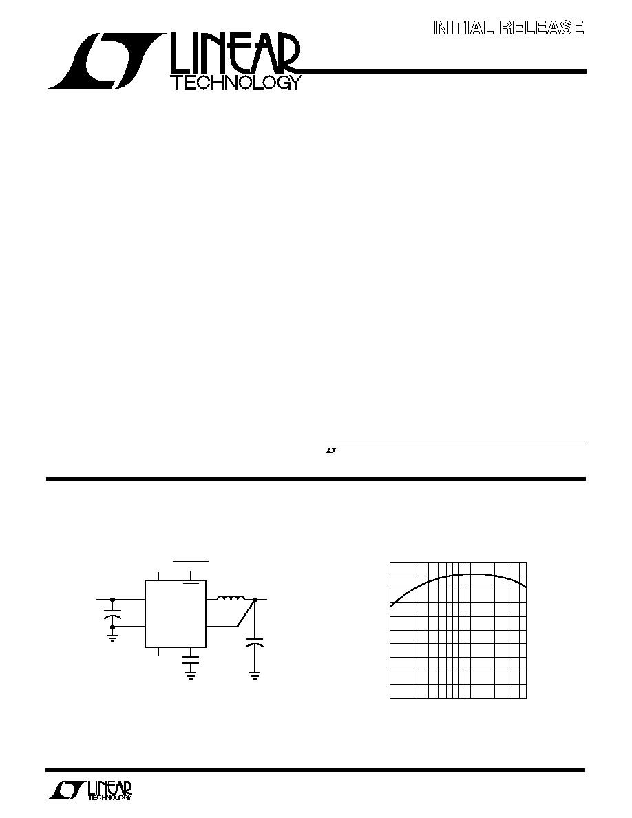
Minimum Part Count 5V to 3.3V Regulator
5V to 3.3V Efficiency
LOAD CURRENT (mA)
10
EFFICIENCY (%)
100
90
80
70
60
50
40
30
20
10
0
100
500
1504 · TA02
I
MAX
SHDN
SS
COMP
V
CC
GND
SW
SENSE
+
C
IN
5V
SHUTDOWN
NC
NC
1000pF
+
C
OUT
3.3V AT 500mA
L
EXT
C
IN
: AVX TPSC226M016R0375
C
OUT
: AVX TAJC476M010
L
EXT
: COILTRONICS CTX50-1P
1504 · TA01
LTC1504-3.3
, LTC and LT are registered trademarks of Linear Technology Corporation.
APPLICATIO
N
S
U
s
Small Portable Digital Systems
s
Active Termination
s
Auxiliary Output Voltage Supplies
s
Minimum Part Count/Size Switchers
2
LTC1504
ABSOLUTE
M
AXI
M
U
M
RATINGS
W
W
W
U
(Note 1)
Supply Voltage (V
CC
to GND) ................................... 10V
Peak Output Current (SW) .......................................
±
1A
Input Voltage (All Other Pins) ......... 0.3V to V
CC
+ 0.3V
Operating Temperature Range ..................... 0
°
C to 70
°
C
Storage Temperature Range ................. 65
°
C to 150
°
C
Lead Temperature (Soldering, 10 sec).................. 300
°
C
W
U
U
PACKAGE/ORDER I FOR ATIO
ORDER PART
NUMBER
1
2
3
4
8
7
6
5
TOP VIEW
COMP
SS
SHDN
FB/SENSE*
I
MAX
V
CC
SW
GND
S8 PACKAGE
8-LEAD PLASTIC SO
*FB FOR LTC1504CS8, SENSE FOR LTC1504CS8-3.3
LTC1504CS8
LTC1504CS8-3.3
T
JMAX
= 115
°
C,
JA
= 90
°
C/W
S8 PART MARKING
1504
15043
Consult factory for Industrial and Military grade parts.
ELECTRICAL CHARACTERISTICS
V
CC
= 5V, T
A
= 25
°
C unless otherwise specified. (Note 2)
SYMBOL
PARAMETER
CONDITIONS
MIN
TYP
MAX
UNITS
V
CC
Minimum Supply Voltage
(Note 7)
q
4
V
V
FB
Feedback Voltage
LTC1504CS8
q
1.25
1.265
1.28
V
V
FB
Feedback Voltage PSRR
Figure 1, 4V
V
CC
10V, LTC1504CS8
q
1.1
1.6
%
V
SENSE
Sense Pin Voltage
LTC1504CS8-3.3
q
3.20
3.30
3.40
V
V
SENSE
Sense Voltage PSRR
Figure 1, 4V
V
CC
10V, LTC1504CS8-3.3
q
1.2
1.8
%
I
CC
Supply Current
Figure 1, V
SHDN
= V
CC
, I
OUT
= 0 (Note 4)
3
mA
Figure 1, V
SHDN
= V
CC
, I
OUT
= 0, V
FB
/V
SENSE
= V
CC
(Note 4)
q
0.3
0.6
mA
V
SHDN
= 0V
q
1.0
20
µ
A
f
OSC
Internal Oscillator Frequency
q
150
200
250
kHz
R
SW
Internal Switch Resistance
q
1.3
2.0
V
IH
SHDN Input High Voltage
q
2.4
V
V
IL
SHDN Input Low Voltage
q
0.8
V
I
IN
SHDN Input Current
q
±
0.1
±
1
µ
A
V
OH
Error Amplifier Positive Swing
Figure 2
q
4.5
4.95
V
V
OL
Error Amplifier Negative Swing
Figure 2
q
0.05
0.5
V
I
OH
, I
OL
Error Amplifier Output Current
Figure 2
q
±
50
±
100
±
200
µ
A
g
mV
Error Amplifier Transconductance
(Note 5)
q
350
600
1100
µ
mho
A
V
Error Amplifier DC Gain
(Note 5)
q
40
48
dB
g
mI
I
LIM
Amplifier Transconductance
(Note 6)
1000
2000
3000
µ
mho
I
MAX
I
MAX
Sink Current
V
IMAX
= V
CC
q
8
12
16
µ
A
I
SS
Soft Start Source Current
V
SS
= 0V
q
8
12
16
µ
A
t
r
, t
f
Output Switch Rise/Fall Time
q
5
50
ns
DC
MAX
Maximum Duty Cycle
V
COMP
= V
CC
q
84
90
%
3
LTC1504
ELECTRICAL CHARACTERISTICS
The
q
denotes specifications which apply over the full operating
temperature range.
Note 1: Absolute Maximum Ratings are those values beyond which the life
of the device may be impaired.
Note 2: All currents into device pins are positive; all currents out of device
pins are negative. All voltages are referenced to ground unless otherwise
specified.
Note 3: This parameter is guaranteed by correlation and is not tested
directly.
Note 4: LTC1504 quiescent current is dominated by the gate drive current
drawn by the onboard power switches. With FB or SENSE pulled to V
CC
the output stage will stop switching and the static quiescent current can be
observed. With FB or SENSE hooked up normally, the output stage will be
switching and total dynamic supply current can be measured.
Note 5: Fixed output parts will appear to have g
mV
and A
V
values 2.6 times
lower than the specified values, due to the internal divider resistors.
Note 6: The I
LIM
amplifier can sink but not source current. Under normal
(not current limited) operation, the I
LIM
output current will be zero.
Note 7: Contact factory for guaranteed specifications at 2.7V supply.
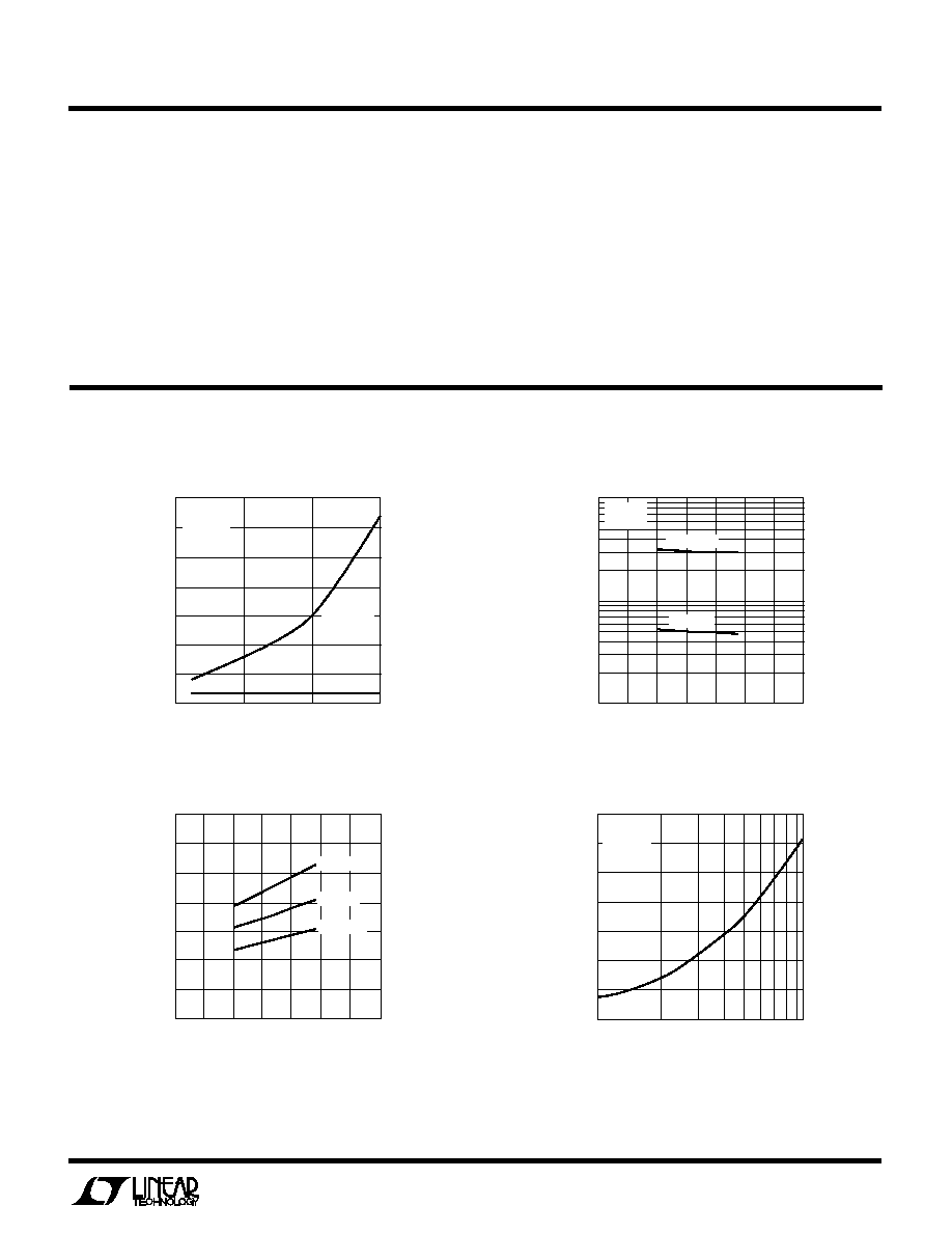
TYPICAL PERFOR
M
A
N
CE CHARACTERISTICS
U
W
TEMPERATURE (
°
C)
50
3.5
3.0
2.5
2.0
1.5
1.0
0.5
0
25
75
1504 · TPC03
25
0
50
100
125
SWITCH ON-RESISTANCE (
)
V
CC
= 10V
V
CC
= 5V
V
CC
= 3.3V
Switch On-Resistance vs
Temperature
Supply Current vs Supply Voltage
SUPPLY VOLTAGE (V)
2.5
1504 · TPC01
5
7.5
10
SUPPLY CURRENT (mA)
14
12
10
8
6
4
2
0
V
FB
= V
OUT
V
FB
= V
CC
T
A
= 25
°
C
I
OUT
= 0
Current Limit Threshold vs R
IMAX
R
IMAX
(
)
10k
CURRENT LIMIT THRESHOLD (mA)
700
600
500
400
300
200
100
0
100k
1504 · TPC04
T
A
= 25
°
C
V
CC
= 5V
TEMPERATURE (
°
C)
50
25
0
25
50
75
100
125
SUPPLY CURRENT (mA)
10
1
0.1
1504 · TPC02
V
FB
= V
OUT
V
FB
= V
CC
V
CC
= 5V
I
OUT
= 0
Supply Current vs Temperature
4
LTC1504
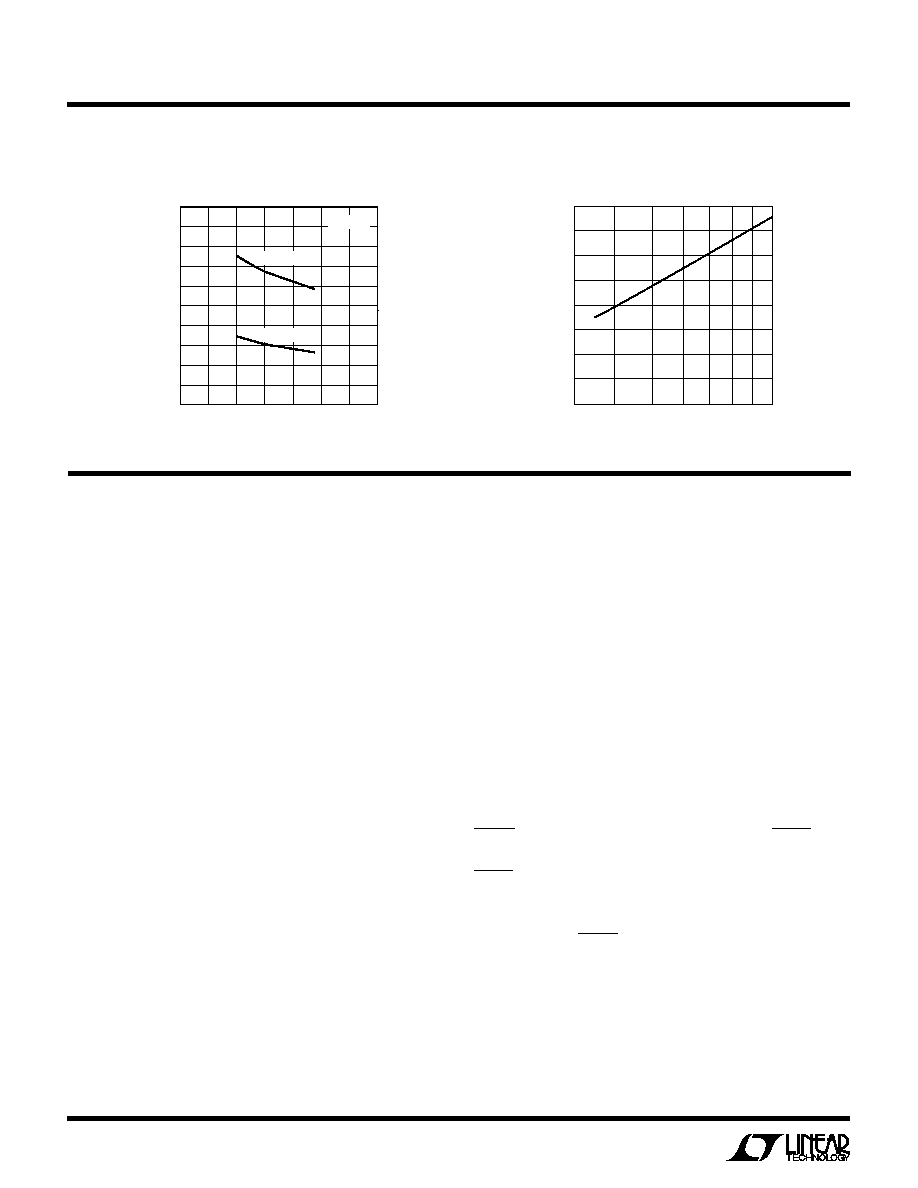
TYPICAL PERFOR
M
A
N
CE CHARACTERISTICS
U
W
Shutdown Threshold vs
Supply Voltage
SUPPLY VOLTAGE (V)
3
5
7
SHUTDOWN PIN THRESHOLD (V)
4.0
3.5
3.0
2.5
2.0
1.5
1.0
0.5
0
10
1504 · TPC07
PI
N
FU
N
CTIO
N
S
U
U
U
as large a copper area as possible to improve thermal
dissipation. See the Thermal Considerations section for
more information.
FB (LTC1504CS8) (Pin 5): Feedback. Connect FB to a
resistor divider from V
OUT
to GND to set the regulated
output voltage. The LTC1504CS8 feedback loop will servo
the FB pin to 1.265V.
SENSE (LTC1504CS8-3.3) (Pin 5): Output Voltage Sense.
Connect directly to the output voltage node. The
LTC1504CS8-3.3 feedback loop will servo SENSE to 3.3V.
SENSE is connected to an internal resistor divider which
will load any external dividers. For output voltages other
than 3.3V, use the LTC1504CS8.
SHDN (Pin 6): Shutdown, Active Low. When SHDN is at a
logic High, the LTC1504 will operate normally. When
SHDN is Low, the LTC1504 ceases all internal operation
and supply current drops below 1
µ
A. In shutdown, the SW
pin is pulled low. This ensures that the output is actively
shut off when SHDN is asserted, but it prevents other
supplies from providing power to the output when the
LTC1504 is inactive. See the Applications Information
section for more details.
SS (Pin 7): Soft Start. Connect an external capacitor
(usually 0.1
µ
F) from SS to GND to limit the output rise time
I
MAX
(Pin 1): Current Limit Set. Connect a resistor from
V
CC
to I
MAX
to set the current limit threshold. An internal
12
µ
A current source from I
MAX
to GND sets the voltage
drop across this resistor. This voltage is compared to the
voltage drop across the internal high-side switch (Q1)
while it is turned on. See the Applications Information
section for more information. To disable current limit,
leave I
MAX
floating.
V
CC
(Pin 2): Power Supply Input. Connect to a power
supply voltage between 4V and 10V. V
CC
requires a low
impedance bypass capacitor to ground, located as close
as possible to the LTC1504. See the Applications Informa-
tion section for details on capacitor selection and
placement.
SW (Pin 3): Power Switch Output. This is the switched
node of the buck circuit. Connect SW to one end of the
external inductor. The other end of the inductor should be
connected to C
OUT
and becomes the regulated output
voltage. Avoid shorting SW to GND or V
CC
.
GND (Pin 4): Ground. Connect to a low impedance ground.
The input and output bypass capacitors and the feedback
resistor divider (adjustable parts only) should be grounded
as close to this pin as possible. Pin 4 acts as a heat sink
in the LTC1504 S0-8 package and should be connected to
Current Limit Threshold vs
Temperature
TEMPERATURE (
°
C)
50
CURRENT LIMIT THRESHOLD (mA)
25
0
25
50
75
1504 · TPC05
125
500
450
400
350
300
250
200
150
100
50
0
100
V
CC
= 5V
R
IMAX
= 47k
R
IMAX
= 22k
5
LTC1504
PI
N
FU
N
CTIO
N
S
U
U
U
during power-up. C
SS
also compensates the current limit
loop, allowing the LTC1504 to enter and exit current limit
cleanly. See the Applications Information section for more
details.
COMP (Pin 8): External Compensation. An external RC
network should be connected to COMP to compensate the
feedback loop. COMP is connected to the output of the
internal error amplifier.
TEST CIRCUITS
I
MAX
SHDN
SS
COMP
V
CC
GND
SW
FB/SENSE
+
C
IN
V
CC
NC
0.01
µ
F
+
C
OUT
V
OUT
L
EXT
C
IN
: AVX TPSE107M016R0125
C
OUT
: SANYO 16CV220GX
L
EXT
: COILCRAFT D03316-473
1504 · TC01
LTC1504
1
µ
F
0.1
µ
F
220pF
7.5k
Figure 1
+
V
REF
LTC1504
COMP
FB/SENSE
A
B
A: TEST V
OL
, I
OL
B: TEST V
OH
, I
OH
1504 · TC02
Figure 2
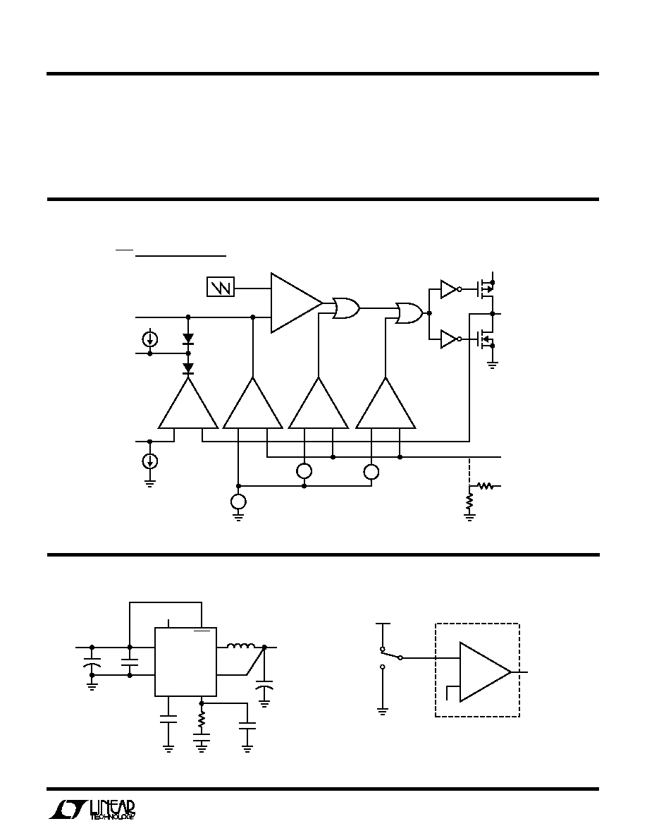
BLOCK DIAGRA
M
W
Figure 3. Block Diagram
+
+
+
MIN
+
MAX
+
FB
+
I
LIM
+
40mV
1.265V
12V
12V
PWM
12.6k
20.4k
Q1
Q2
SW
FB
(ADJ ONLY)
SENSE
(3.3V ONLY)
SAW
I
MAX
SS
COMP
SHDN
1504 · BD
+
40mV
V
REF
V
CC
TO INTERNAL BLOCKS