 | ÐлекÑÑоннÑй компоненÑ: LTC1515 | СкаÑаÑÑ:  PDF PDF  ZIP ZIP |
/home/web/doc/html/liner/177758

1
LTC1515 Series
Step-Up/Step-Down
Switched Capacitor DC/DC
Converters with Reset
Daisy-Chained Control Outputs
FEATURES
The LTC
®
1515, LTC1515-3/5 and LTC1515-3.3/5 are
micropower switched capacitor DC/DC converters that
produce a regulated output voltage by either stepping up
or stepping down the input voltage. Output voltage is
adjustable using an external resistor divider (LTC1515) or
programmable to either 3V/5V (LTC1515-3/5) or 3.3V/5V
(LTC1515-3.3/5) using a logic pin.
A unique architecture allows the parts to accommodate a
wide input voltage range (2V to 10V) while maintaining
±
4% regulation. Additional circuitry prevents excessive
inrush current and output voltage ripple when large V
IN
to
V
OUT
differentials are present.
An internal power-on reset circuit forces the POR pin low
on initial power-up. The POR output remains low until
200ms (typ) after V
OUT
is in regulation.
The parts are short-circuit and overtemperature protected.
Battery life is maximized by very low operating currents
(I
CC
= 60
µ
A typ, I
CC
< 1
µ
A in shutdown). All three parts are
available in an SO-8 package.
DESCRIPTIO
N
U
s
Adjustable/Selectable 3V, 3.3V or 5V
Output Voltages
s
2V to 10V Input Voltage Range
s
Up to 50mA Output Current
s
Only Three External Capacitors Required
s
Soft Start Limits Inrush Current at Turn-On
s
Low Operating Current: 60
µ
A
s
Very Low Shutdown Current: < 1
µ
A
s
Shutdown Disconnects Load from V
IN
s
V
OUT
Programmable to 3V/5V or 3.3V/5V
s
Short-Circuit and Overtemperature Protected
s
650kHz Switching Frequency
s
Open-Drain Power-On Reset Output
s
Available in SO-8 Package
TYPICAL APPLICATIO
N
U
APPLICATIO
N
S
U
s
SIM Interface in GSM Cellular Telephones
s
Smart Card Readers
s
Local Power Supplies
s
Portable Equipment
, LTC and LT are registered trademarks of Linear Technology Corporation.
Programmable 3.3V/5V Power Supply with Power-On Reset
SHDN
POR
GND
5/3
V
OUT
V
IN
C1
C1
+
LTC1515-3.3/5
1
2
3
4
8
7
6
5
0.22
µ
F
10
µ
F
10
µ
F
V
IN
4-CELL
NiCd
100k
V
OUT
= 3.3V OR 5V
I
OUT
= 50mA
ON OFF
RESET
5V 3.3V
LTC1515 · TA01
+
+
LTC1515-X 5V Output vs Input Voltage
INPUT VOLTAGE (V)
2
OUTPUT VOLTAGE (V)
10
LT1515 · TA02
4
6
8
3
5
7
9
5.2
5.1
5.0
4.9
4.8
I
OUT
= 10mA
5/3 = 3V
2
LTC1515 Series
ABSOLUTE
M
AXI
M
U
M
RATINGS
W
W
W
U
(Note 1)
V
IN
to GND ................................................ 0.3V to 12V
V
OUT
to GND ............................................. 0.3V to 12V
SHDN, 5/3, FB to GND .............................. 0.3V to 12V
V
OUT
Short-Circuit Duration ............................. Indefinite
Operating Temperature Range
Commercial ............................................. 0
°
C to 70
°
C
Industrial ............................................ 40
°
C to 85
°
C
Storage Temperature Range ................ 65
°
C to 150
°
C
Lead Temperature (Soldering, 10 sec)................. 300
°
C
W
U
U
PACKAGE/ORDER I FOR ATIO
ORDER PART NUMBER
ORDER PART
NUMBER
S8 PART MARKING
LTC1515CS8-3/5
LTC1515CS8-3.3/5
LTC1515IS8-3/5
LTC1515IS8-3.3/5
151535
515335
515I35
15I335
T
JMAX
= 125
°
C,
JA
= 110
°
C/W
1
2
3
4
8
7
6
5
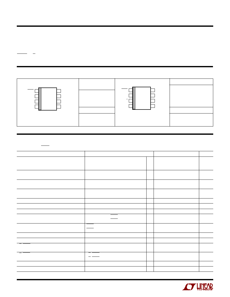
TOP VIEW
V
OUT
V
IN
C1
+
C1
SHDN
POR
5/3
GND
S8 PACKAGE
8-LEAD PLASTIC SO
LTC1515CS8
LTC1515IS8
S8 PART MARKING
1515
1515I
T
JMAX
= 125
°
C,
JA
= 110
°
C/W
1
2
3
4
8
7
6
5
TOP VIEW
V
OUT
V
IN
C1
+
C1
SHDN
POR
FB
GND
S8 PACKAGE
8-LEAD PLASTIC SO
Consult factory for Military grade parts.
ELECTRICAL CHARACTERISTICS
V
IN
= 2V to 10V, SHDN = 3V, C1 = 0.22
µ
F, C
IN
= C
OUT
= 10
µ
F unless otherwise noted (Note 2).
PARAMETER
CONDITIONS
MIN
TYP
MAX
UNITS
V
IN
Operating Voltage
V
OUT
= 5V
q
2.7
10
V
V
OUT
= 3V/3.3V
q
2.0
8
V
V
OUT
= ADJ
q
2.0
10
V
V
OUT
= 3V (LTC1515-3/5)
2V
V
IN
8V, I
OUT
15mA
q
2.88
3.0
3.12
V
3V
V
IN
8V, I
OUT
50mA
q
2.88
3.0
3.12
V
V
OUT
= 3.3V (LTC1515-3.3/5)
2V
V
IN
8V, I
OUT
15mA
q
3.17
3.3
3.43
V
3V
V
IN
8V, I
OUT
50mA
q
3.17
3.3
3.43
V
V
OUT
= 5V (LTC1515-3/5, LTC1515-3.3/5)
2.7V
V
IN
10V, I
OUT
15mA
q
4.8
5.0
5.2
V
3.3V
V
IN
10V, I
OUT
50mA
q
4.8
5.0
5.2
V
V
FB
Feedback Voltage
LTC1515, V
FB
Ramping Negative
q
1.190
1.232
1.275
V
V
FB
Feedback Hysteresis
LTC1515
1
%
Effective Output Resistance
LTC1515, V
IN
= 3V, Step-Up Mode
q
30
V
IN
Operating Current
V
IN
5V, I
OUT
= 0, SHDN = 3V
q
60
100
µ
A
V
IN
> 5V, I
OUT
= 0, SHDN = 3V
q
75
135
µ
A
V
IN
Shutdown Current
SHDN = 0V, V
IN
5V
q
1
µ
A
SHDN = 0V, V
IN
> 5V
25
µ
A
Output Ripple
Full Load (Note 2)
100
mV
P-P
Switching Frequency
Full Load
q
500
650
800
kHz
5/3, SHDN Input Threshold
V
IL
q
0.4
1.0
V
V
IH
q
1.0
1.6
V
5/3, SHDN Input Current
5/3, SHDN = V
IN
q
1
1
µ
A
5/3, SHDN = 0V
q
1
1
µ
A
FB Input Current
FB = 1.232V
q
50
50
nA
POR Output Low Voltage
I
SINK
= 100
µ
A, V
IN
= 3V
q
0.05
0.4
V
3
LTC1515 Series
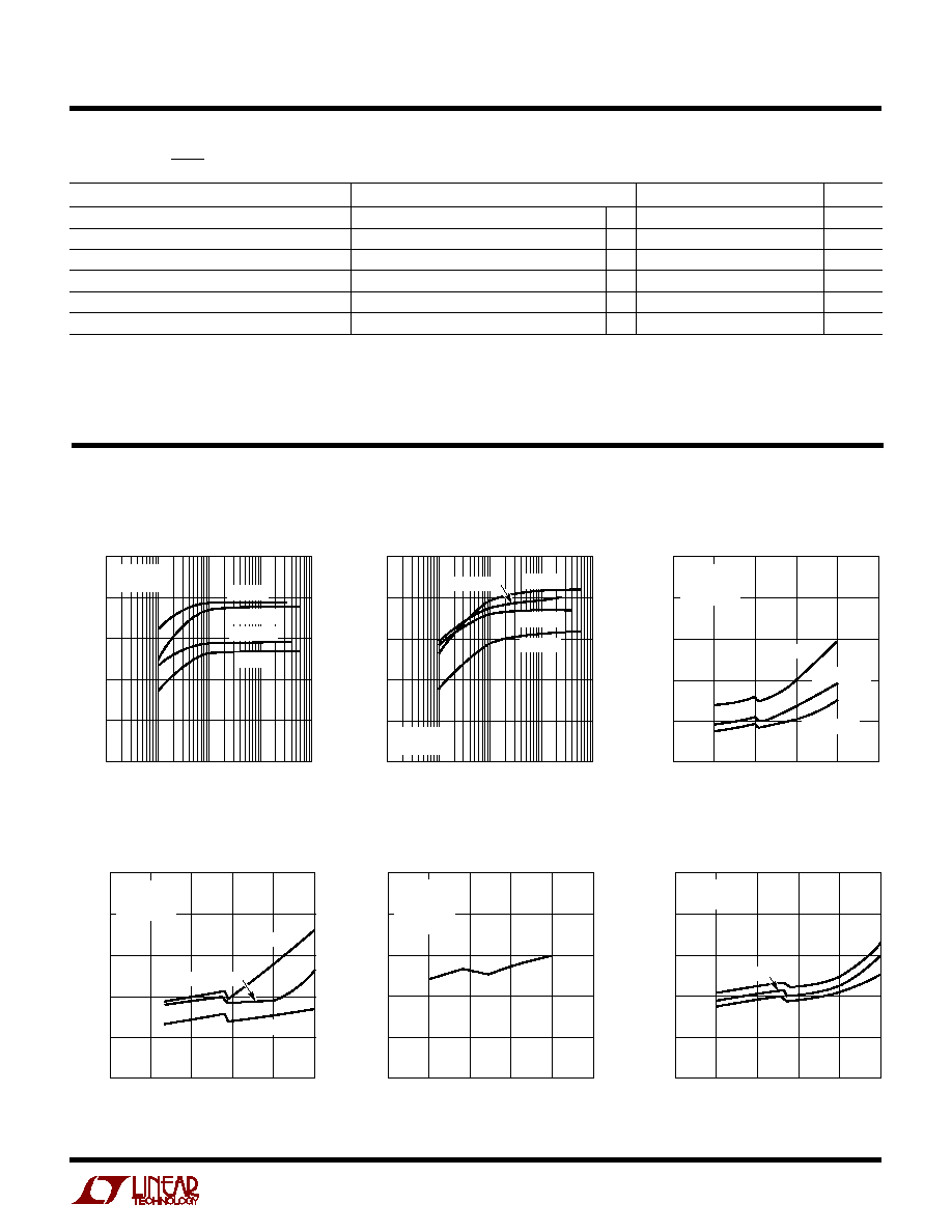
LTC1515-X 3.3V Output Voltage
vs Input Voltage
INPUT VOLTAGE (V)
0
OPERATING CURRENT (
µ
A)
120
100
80
60
40
20
8
1515 G06
2
4
6
10
85
°
C
40
°
C
25
°
C
V
OUT
= 5V
I
OUT
= 0mA
LTC1515-X Operating Current
vs Input Voltage
TYPICAL PERFOR
M
A
N
CE CHARACTERISTICS
U
W
LTC1515-X
5V Efficiency vs Output Current
OUTPUT CURRENT (mA)
EFFICIENCY (%)
0.01
1
10
1515 G02
0.1
100
100
80
60
40
20
0
V
OUT
= 5V
T
A
= 25
°
C
V
IN
= 8V
V
IN
= 3.3V
V
IN
= 6V
V
IN
= 2.7V
LTC1515-X 3.3V Output Voltage
Ripple vs Input Voltage
ELECTRICAL CHARACTERISTICS
V
IN
= 2V to 10V, SHDN = 3V, C1 = 0.22
µ
F, C
IN
= C
OUT
= 10
µ
F unless otherwise noted (Note 2).
PARAMETER
CONDITIONS
MIN
TYP
MAX
UNITS
POR Leakage Current
V
POR
= 5V
q
1
1
µ
A
POR Trip Point (With Respect to V
OUT
)
V
OUT
Ramping Negative
q
10
7.5
5
%
POR Trip Point Hysteresis
1
%
I
OUT
Short-Circuit Current
V
OUT
= 0V
q
12
40
mA
t
ON
Soft Start Turn-On Time
4
ms
POR Delay
After V
OUT
Above POR Threshold
q
140
200
280
ms
The
q
denotes specifications which apply over the full operating
temperature range.
Note 1: Absolute Maximum Ratings are those values beyond which the life
of the device may be impaired.
Note 2: For V
IN
8V, C
OUT
= 22
µ
F.
INPUT VOLTAGE (V)
0
OUTPUT VOLTAGE RIPPLE (mV
P-P
)
250
200
150
100
50
0
8
1515 G03
2
4
6
10
V
OUT
= 3.3V
I
OUT
= 10mA
T
A
= 25
°
C
C
OUT
= 10
µ
F
C
OUT
= 22
µ
F
C
OUT
= 47
µ
F
INPUT VOLTAGE (V)
0
OUTPUT VOLTAGE RIPPLE (mV
P-P
)
250
200
150
100
50
0
8
1515 G04
2
4
6
10
V
OUT
= 5V
I
OUT
= 10mA
T
A
= 25
°
C
C
OUT
= 10
µ
F
C
OUT
= 47
µ
F
C
OUT
= 22
µ
F
LTC1515-X 5V Output Voltage
Ripple vs Input Voltage
LTC1515-X
3.3V Efficiency vs Output Current
OUTPUT CURRENT (mA)
EFFICIENCY (%)
0.01
1
10
1515 G01
0.1
100
100
80
60
40
20
0
V
OUT
= 3.3V
T
A
= 25
°
C
V
IN
= 2V
V
IN
= 4.4V
V
IN
= 2.7V
V
IN
= 6V
INPUT VOLTAGE (V)
0
OUTPUT VOLTAGE (V)
3.45
3.40
3.35
3.30
3.25
3.20
8
1515 G05
2
4
6
10
V
OUT
= 3.3V
I
OUT
= 10mA
C
OUT
= 10
µ
F
T
A
= 25
°
C
4
LTC1515 Series
TYPICAL PERFOR
M
A
N
CE CHARACTERISTICS
U
W
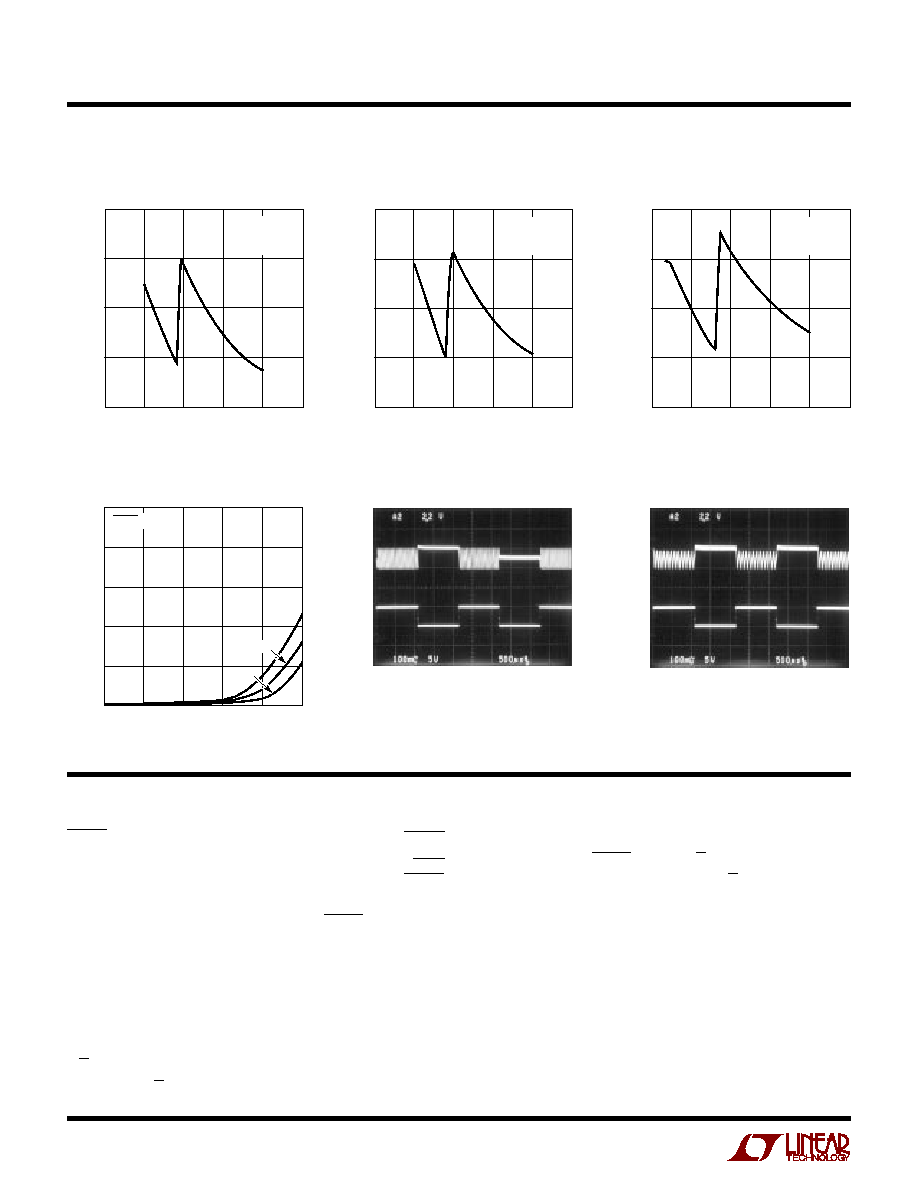
LTC1515-X Shutdown Supply
Current vs Input Voltage
LTC1515-X Step-Down Mode
5V Load Transient Response
INPUT VOLTAGE (V)
0
POSITIVE SUPPLY CURRENT (
µ
A)
25
20
15
10
5
0
8
1515 G12
2
4
6
10
85
°
C
SHDN = 0V
40
°
C
25
°
C
V
OUT
AC COUPLED
100mV/DIV
I
OUT
50mA/DIV
V
IN
= 8V, V
OUT
= 5V, C
OUT
= 10
µ
F, T
A
= 25
°
C
1515 G10
50mA
0mA
V
OUT
AC COUPLED
100mV/DIV
I
OUT
50mA/DIV
LTC1515-X Step-Up Mode
5V Load Transient Response
V
IN
= 3.3V, V
OUT
= 5V, C
OUT
= 10
µ
F, T
A
= 25
°
C
1515 G11
low will force V
OUT
to 3V (LTC1515-3/5) or 3.3V (LTC1515-
3.3/5). As with the SHDN pin, the 5/3 pin may be driven with
3V logic over the entire V
IN
range. The 5/3 pin may not float.
FB (LTC1515) (Pin 3): Feedback Input. The voltage on this
pin is compared to the internal reference voltage (1.232V)
to keep the output in regulation. An external resistor divider
is required between V
OUT
and FB to adjust the output
voltage. Total divider resistance should not exceed 2M.
GND (Pin 4): Ground. Should be tied to a ground plane for
best performance.
C1
(Pin 5): Charge Pump Flying Capacitor, Negative
Terminal.
SHDN (Pin 1): Shutdown Input. A logic low on the SHDN
pin puts the part into shutdown mode. A logic high (V
SHDN
1.6V) enables the part. At high V
IN
voltages, the SHDN
pin may still be controlled with 3V logic without causing a
large rise in V
IN
quiescent current. The SHDN pin may not
float; connect to V
IN
if unused.
POR (Pin 2): Open-Drain Power-On Reset Output. This pin
will pull low upon initial power-up, during shutdown or
until V
OUT
has been within 6.5% of its regulated value for
more than 200ms typ.
5/3 (LTC1515-X) (Pin 3): Output Voltage Select. A logic
high on the 5/3 pin will force V
OUT
to regulate to 5V. A logic
PI
N
FU
N
CTIO
N
S
U
U
U
INPUT VOLTAGE (V)
0
EFFICIENCY (%)
100
80
60
40
20
8
1515 G09
2
4
6
10
V
OUT
= 3V
I
OUT
= 10mA
T
A
= 25
°
C
LTC1515-X
3V Efficiency vs Input Voltage
LTC1515-X
5V Efficiency vs Input Voltage
INPUT VOLTAGE (V)
2
EFFICIENCY (%)
100
80
60
40
20
10
1515 G08
4
6
8
12
V
OUT
= 5V
I
OUT
= 10mA
TA = 25
°
C
INPUT VOLTAGE (V)
0
EFFICIENCY (%)
100
80
60
40
20
8
1515 G07
2
4
6
10
V
OUT
= 3.3V
I
OUT
= 10mA
TA = 25
°
C
LTC1515-X
3.3V Efficiency vs Input Voltage
5
LTC1515 Series
PI
N
FU
N
CTIO
N
S
U
U
U
C1
+
(Pin 6): Charge Pump Flying Capacitor, Positive
Terminal.
V
IN
(Pin 7): Charge Pump Input Voltage. May be between
2V and 10V. V
IN
should be bypassed with a
10
µ
F low
ESR capacitor as close as possible to the pin for best
performance.
V
OUT
(Pin 8): Regulated Output Voltage. Pin selectable to
either 3V/5V, 3.3V/5V or adjustable using an external
resistor divider (LTC1515). V
OUT
should be bypassed with
a
10
µ
F low ESR capacitor as close as possible to the pin
for best performance.
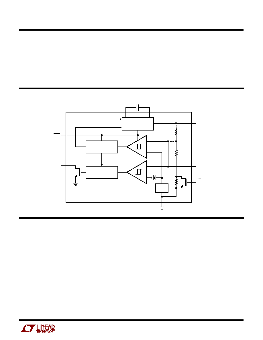
BLOCK DIGRA
M
W
W
SI PLIFIED
APPLICATIO
N
S I
N
FOR
M
ATIO
N
W
U
U
U
Regulator Operation
The regulator section of the LTC1515, LTC1515-3/5 and
LTC1515-3.3/5 consists of a charge pump, reference,
comparator and some logic. The divided down output
voltage is compared to the internal reference voltage.
When the divided output drops below the reference volt-
age, the charge pump is enabled, which boosts the output
back into regulation. Hysteresis in the comparator forces
the regulator to burst on and off and causes approximately
100mV of peak-to-peak ripple to appear at the output. By
enabling the charge pump only when needed, the parts
achieve high efficiencies with low output load currents.
Each part's charge pump has a unique architecture that
allows the input voltage to be either stepped up or stepped
down to produce a regulated output. Internal circuitry
senses the V
IN
to V
OUT
differential voltage and controls the
charge pump operating mode. In addition, the effective
output impedance of the charge pump is internally
adjusted to prevent large inrush currents and allow for a
wide input voltage range. When the input voltage is lower
than the output voltage, the charge pump operates as a
step-up voltage doubler. When the input voltage is greater
than the output, the charge pump operates as a step-down
gated switch.
+
+
V
OS
1.232V
V
REF
650kHz
OSCILLATOR
RESET
COUNTER
STEP-UP/STEP-DOWN
CHARGE PUMP
V
IN
SHDN
POR
GND
C1
C1
+
V
OUT
(LTC1515-X)
(LTC1515-X)
LTC1515 · BD
FB
(LTC1515)
5/3
(LTC1515-X)
EN
EN