 | –≠–ª–µ–∫—Ç—Ä–æ–Ω–Ω—ã–π –∫–æ–º–ø–æ–Ω–µ–Ω—Ç: LTC1604C | –°–∫–∞—á–∞—Ç—å:  PDF PDF  ZIP ZIP |
1
LTC1604
High Speed, 16-Bit, 333ksps
Sampling A/D Converter
with Shutdown
APPLICATIO
N
S
U
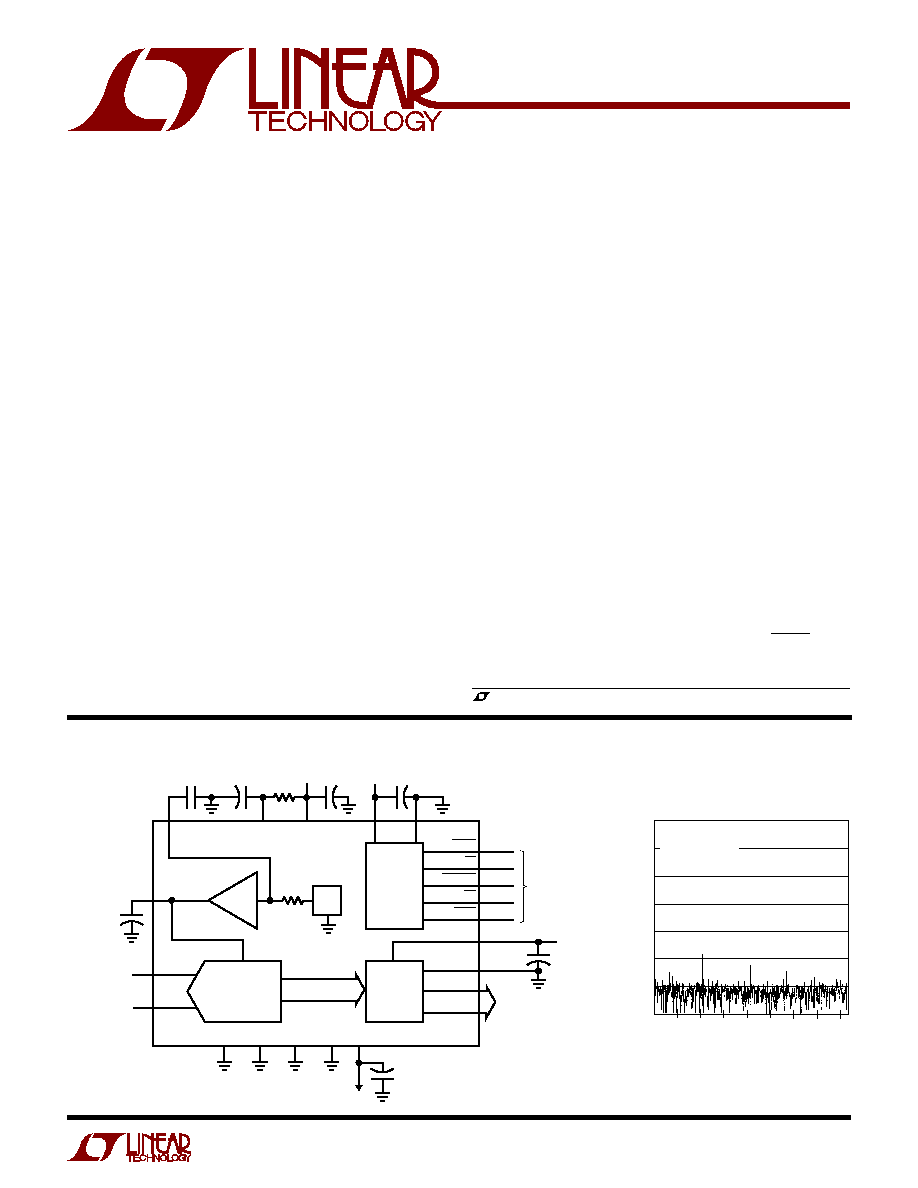
The LTC
Æ
1604 is a 333ksps, 16-bit sampling A/D con-
verter that draws only 220mW from
±
5V supplies. This
high performance device includes a high dynamic range
sample-and-hold, a precision reference and a high speed
parallel output. Two digitally selectable power shutdown
modes provide power savings for low power systems.
The LTC1604's full-scale input range is
±
2.5V. Outstand-
ing AC performance includes 90dB S/(N+D) and ≠ 100dB
THD at a sample rate of 333ksps.
The unique differential input sample-and-hold can acquire
single-ended or differential input signals up to its 15MHz
bandwidth. The 68dB common mode rejection allows
users to eliminate ground loops and common mode noise
by measuring signals differentially from the source.
The ADC has
µ
P compatible,16-bit parallel output port.
There is no pipeline delay in conversion results. A separate
convert start input and a data ready signal (BUSY) ease
connections to FlFOs, DSPs and microprocessors.
FEATURES
s
A Complete, 333ksps 16-Bit ADC
s
90dB S/(N+D) and ≠100dB THD (Typ)
s
Power Dissipation: 220mW (Typ)
s
No Pipeline Delay
s
No Missing Codes over Temperature
s
Nap (7mW) and Sleep (10
µ
W) Shutdown Modes
s
Operates with Internal 15ppm/
∞
C Reference
or External Reference
s
True Differential Inputs Reject Common Mode Noise
s
5MHz Full Power Bandwidth
s
±
2.5V Bipolar Input Range
s
36-Pin SSOP Package
DESCRIPTIO
N
U
, LTC and LT are registered trademarks of Linear Technology Corporation.
TYPICAL APPLICATIO
N
U
FREQUENCY (kHz)
0
AMPLITUDE (dB)
120
1604 TA02
40
80
160
0
≠20
≠40
≠60
≠80
≠100
≠120
≠140
20
60
100
140
f
SAMPLE
= 333kHz
f
IN
= 100kHz
SINAD = 89dB
THD = ≠96dB
LTC1604 4096 Point FFT
s
Telecommunications
s
Digital Signal Processing
s
Multiplexed Data Acquisition Systems
s
High Speed Data Acquisition
s
Spectrum Analysis
s
Imaging Systems
2.2
µ
F
10
µ
F
10
µ
F
10
47
µ
F
4
6
DIFFERENTIAL
ANALOG INPUT
±
2.5V
REFCOMP
4.375V
CONTROL
LOGIC
AND
TIMING
B15 TO B0
16-BIT
SAMPLING
ADC
≠
+
10
µ
F
5V OR
3V
µ
P
CONTROL
LINES
D15 TO D0
OUTPUT
BUFFERS
16-BIT
PARALLEL
BUS
11 TO 26
1604 TA01
OGND
OV
DD
28
29
1
2
A
IN
+
A
IN
≠
SHDN
CS
CONVST
RD
BUSY
33
32
31
30
27
7.5k
3
36
35
10
9
5V
5V
AV
DD
AV
DD
DV
DD
DGND
V
REF
8
AGND
AGND
7
AGND
5
AGND
34
≠5V
V
SS
10
µ
F
2.5V
REF
10
µ
F
1.75X
+
+
+
+
+
+
2
LTC1604
ABSOLUTE
M
AXI
M
U
M
RATINGS
W
W
W
U
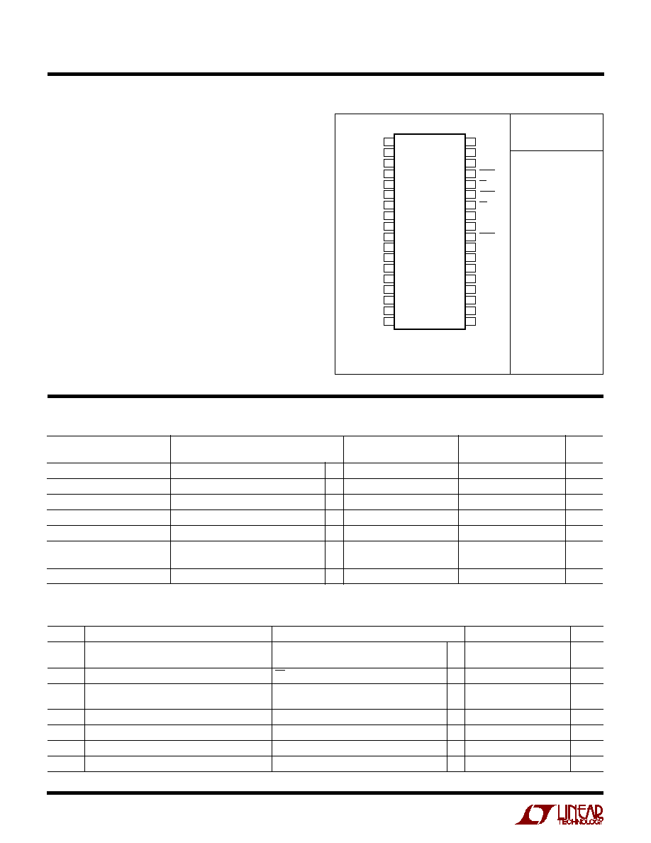
PACKAGE/ORDER I
N
FOR
M
ATIO
N
W
U
U
ORDER
PART NUMBER
AV
DD
= DV
DD
= OV
DD
= V
DD
(Notes 1, 2)
Supply Voltage (V
DD
) ................................................ 6V
Negative Supply Voltage (V
SS
)................................ ≠ 6V
Total Supply Voltage (V
DD
to V
SS
) .......................... 12V
Analog Input Voltage
(Note 3) ......................... (V
SS
≠ 0.3V) to (V
DD
+ 0.3V)
V
REF
Voltage (Note 4) ................. ≠ 0.3V to (V
DD
+ 0.3V)
REFCOMP Voltage (Note 4) ......... ≠ 0.3V to (V
DD
+ 0.3V)
Digital Input Voltage (Note 4) ....................≠ 0.3V to 10V
Digital Output Voltage .................. ≠ 0.3V to (V
DD
+ 0.3V)
Power Dissipation ............................................. 500mW
Operating Temperature Range
LTC1604C............................................... 0
∞
C to 70
∞
C
LTC1604I ............................................ ≠ 40
∞
C to 85
∞
C
Storage Temperature Range ................ ≠ 65
∞
C to 150
∞
C
Lead Temperature (Soldering, 10 sec)................. 300
∞
C
T
JMAX
= 125
∞
C,
JA
= 95
∞
C/W
Consult factory for Military grade parts.
C
C
HARA TERISTICS
CO
U
VERTER
With Internal Reference (Notes 5, 6)
LTC1604
LTC1604A
PARAMETER
CONDITIONS
MIN
TYP
MAX
MIN
TYP
MAX
UNITS
Resolution (No Missing Codes)
q
15
16
16
16
Bits
Integral Linearity Error
(Note 7)
q
±
1
±
4
±
0.5
±
2
LSB
Transition Noise
(Note 8)
0.7
0.7
LSB
Offset Error
(Note 9)
q
±
0.05
±
0.125
±
0.05
±
0.125
%
Offset Tempco
(Note 9)
0.5
0.5
ppm/
∞
C
Full-Scale Error
Internal Reference
±
0.125
±
0.25
±
0.125
±
0.25
%
External Reference
±
0.25
±
0.25
%
Full-Scale Tempco
I
OUT
(Reference) = 0, Internal Reference
±
15
±
15
ppm/
∞
C
LTC1604CG
LTC1604IG
LTC1604ACG
LTC1604AIG
SYMBOL
PARAMETER
CONDITIONS
MIN
TYP
MAX
UNITS
V
IN
Analog Input Range (Note 2)
4.75
V
DD
5.25V, ≠ 5.25
V
SS
≠ 4.75V,
±
2.5
V
V
SS
(A
IN
≠
, A
IN
+
)
AV
DD
I
IN
Analog Input Leakage Current
CS = High
q
±
1
µ
A
C
IN
Analog Input Capacitance
Between Conversions
43
pF
During Conversions
5
pF
t
ACQ
Sample-and-Hold Acquisition Time
380
ns
t
AP
Sample-and-Hold Acquisition Delay Time
≠ 1.5
ns
t
jitter
Sample-and-Hold Acquisition Delay Time Jitter
5
ps
RMS
CMRR
Analog Input Common Mode Rejection Ratio
≠ 2.5V < (A
IN
≠
= A
IN
+
) < 2.5V
68
dB
PUT
U
I
A
A
U
LOG
1
2
3
4
5
6
7
8
9
10
11
12
13
14
15
16
17
18
TOP VIEW
G PACKAGE
36-LEAD PLASTIC SSOP
36
35
34
33
32
31
30
29
28
27
26
25
24
23
22
21
20
19
AV
DD
AV
DD
V
SS
SHDN
CS
CONV
RD
OV
DD
OGND
BUSY
D0
D1
D2
D3
D4
D5
D6
D7
A
IN
+
A
IN
≠
V
REF
REFCOMP
AGND
AGND
AGND
AGND
DV
DD
DGND
D15 (MSB)
D14
D13
D12
D11
D10
D9
D8
3
LTC1604
DY
A
IC ACCURACY
U
W
(Note 5)
LTC1604
LTC1604A
SYMBOL
PARAMETER
CONDITIONS
MIN
TYP
MAX
MIN
TYP
MAX
UNITS
S/N
Signal-to-Noise Ratio
5kHz Input Signal
q
90
87
90
dB
100kHz Input Signal
90
90
dB
S/(N + D) Signal-to-(Noise + Distortion) Ratio
5kHz Input Signal
90
90
dB
100kHz Input Signal (Note 10)
q
89
84
89
dB
THD
Total Harmonic Distortion
5kHz Input Signal
≠100
≠ 100
dB
Up to 5th Harmonic
100kHz Input Signal
q
≠ 94
≠ 94
≠ 88
dB
SFDR
Spurious Free Dynamic Range
100kHz Input Signal
96
96
dB
IMD
Intermodulation Distortion
f
IN1
= 29.37kHz, f
IN2
= 32.446kHz
≠ 88
≠ 88
dB
Full Power Bandwidth
5
5
MHz
Full Linear Bandwidth (S/(N + D)
84dB
350
350
kHz
(Note 5)
PARAMETER
CONDITIONS
MIN
TYP
MAX
UNITS
V
REF
Output Voltage
I
OUT
= 0
2.475
2.500
2.515
V
V
REF
Output Tempco
I
OUT
= 0
±
15
ppm/
∞
C
V
REF
Line Regulation
4.75
V
DD
5.25V
0.01
LSB/V
≠ 5.25V
V
SS
≠ 4.75V
0.01
LSB/V
V
REF
Output Resistance
0
I
OUT
1mA
7.5
k
REFCOMP Output Voltage
I
OUT
= 0
4.375
V
I TER AL REFERE CE CHARACTERISTICS
U
U
U
SYMBOL
PARAMETER
CONDITIONS
MIN
TYP
MAX
UNITS
V
IH
High Level Input Voltage
V
DD
= 5.25V
q
2.4
V
V
IL
Low Level Input Voltage
V
DD
= 4.75V
q
0.8
V
I
IN
Digital Input Current
V
IN
= 0V to V
DD
q
±
1 0
µ
A
C
IN
Digital Input Capacitance
5
pF
V
OH
High Level Output Voltage
V
DD
= 4.75V, I
OUT
= ≠ 10
µ
A
4.5
V
V
DD
= 4.75V, I
OUT
= ≠ 400
µ
A
q
4.0
V
V
OL
Low Level Output Voltage
V
DD
= 4.75V, I
OUT
= 160
µ
A
0.05
V
V
DD
= 4.75V, I
OUT
= 1.6mA
q
0.10
0.4
V
I
OZ
Hi-Z Output Leakage D15 to D0
V
OUT
= 0V to V
DD
, CS High
q
±
10
µ
A
C
OZ
Hi-Z Output Capacitance D15 to D0
CS High (Note 11)
q
15
pF
I
SOURCE
Output Source Current
V
OUT
= 0V
≠ 1 0
mA
I
SINK
Output Sink Current
V
OUT
= V
DD
10
mA
(Note 5)
DIGITAL I PUTS A D DIGITAL OUTPUTS
U
U
4
LTC1604
SYMBOL
PARAMETER
CONDITIONS
MIN
TYP
MAX
UNITS
V
DD
Positive Supply Voltage
(Notes 12, 13)
4.75
5.25
V
V
SS
Negative Supply Voltage
(Note 12)
≠ 4.75
≠ 5.25
V
I
DD
Positive Supply Current
CS = RD = 0V
q
18
30
mA
Nap Mode
CS = 0V, SHDN = 0V
1.5
2.4
mA
Sleep Mode
CS = 5V, SHDN = 0V
1
100
µ
A
I
SS
Negative Supply Current
CS = RD = 0V
q
26
40
mA
Nap Mode
CS = 0V, SHDN = 0V
1
100
µ
A
Sleep Mode
CS = 5V, SHDN = 0V
1
100
µ
A
P
D
Power Dissipation
CS = RD = 0V
q
220
350
mW
Nap Mode
CS = 0V, SHDN = 0V
7.5
12
mW
Sleep Mode
CS = 5V, SHDN = 0V
0.01
1
mW
POWER REQUIRE E TS
W
U
TI I G CHARACTERISTICS
U
W
(Note 5)
SYMBOL
PARAMETER
CONDITIONS
MIN
TYP
MAX
UNITS
f
SMPL(MAX)
Maximum Sampling Frequency
q
333
kHz
t
CONV
Conversion Time
q
1.5
2.45
2.8
µ
s
t
ACQ
Acquisition Time
(Note 11)
q
480
ns
t
ACQ+CONV
Throughput Time (Acquisition + Conversion)
q
3
µ
s
t
1
CS to RD Setup Time
(Notes 11, 12)
q
0
ns
t
2
CS
to CONVST
Setup Time
(Notes 11, 12)
q
10
ns
t
3
SHDN
to CS
Setup Time
(Notes 11, 12)
q
10
ns
t
4
SHDN
to CONVST
Wake-Up Time
CS = Low (Note 12)
400
ns
t
5
CONVST Low Time
(Note 12)
q
40
ns
t
6
CONVST to BUSY Delay
C
L
= 25pF
36
ns
q
80
ns
t
7
Data Ready Before BUSY
60
ns
q
32
ns
t
8
Delay Between Conversions
(Note 12)
q
200
ns
t
9
Wait Time RD
After BUSY
(Note 12)
q
≠ 5
ns
t
10
Data Access Time After RD
C
L
= 25pF
40
50
ns
q
60
ns
C
L
= 100pF
45
60
ns
q
75
ns
t
11
Bus Relinquish Time
50
60
ns
LTC1604C
q
70
ns
LTC1604I
q
75
ns
t
12
RD Low Time
(Note 12)
q
t
10
ns
t
13
CONVST High Time
(Note 12)
q
40
ns
t
14
Aperture Delay of Sample-and-Hold
2
ns
(Note 5)
5
LTC1604
The
q
denotes specifications that apply over the full operating temperature
range.
Note 1: Absolute Maximum Ratings are those values beyond which the life
of a device may be impaired.
Note 2: All voltage values are with respect to ground with DGND, OGND
and AGND wired together unless otherwise noted.
Note 3: When these pin voltages are taken below V
SS
or above V
DD
, they
will be clamped by internal diodes. This product can handle input currents
greater than 100mA below V
SS
or above V
DD
without latchup.
Note 4: When these pin voltages are taken below V
SS
, they will be clamped
by internal diodes. This product can handle input currents greater than
100mA below V
SS
without latchup. These pins are not clamped to V
DD
.
Note 5: V
DD
= 5V, V
SS
= ≠ 5V, f
SMPL
= 333kHz, and t
r
= t
f
= 5ns unless
otherwise specified.
Note 6: Linearity, offset and full-scale specification apply for a single-
ended A
IN
+
input with A
IN
≠
grounded.
TI I G CHARACTERISTICS
U
W
(Note 5)
Note 7: Integral nonlinearity is defined as the deviation of a code from a
straight line passing through the actual endpoints of the transfer curve.
The deviation is measured from the center of the quantization band.
Note 8: Typical RMS noise at the code transitions. See Figure 17 for
histogram.
Note 9: Bipolar offset is the offset voltage measured from ≠ 0.5LSB when
the output code flickers between 0000 0000 0000 0000 and 1111 1111
1111 1111.
Note 10: Signal-to-Noise Ratio (SNR) is measured at 5kHz and distortion
is measured at 100kHz. These results are used to calculate Signal-to-Nosie
Plus Distortion (SINAD).
Note 11: Guaranteed by design, not subject to test.
Note 12: Recommended operating conditions.
Note 13: The falling CONVST edge starts a conversion. If CONVST returns
high at a critical point during the conversion it can create small errors. For
best performance ensure that CONVST returns high either within 250ns
after conversion start or after BUSY rises.
TYPICAL PERFOR
M
A
N
CE CHARACTERISTICS
U
W
Spurious-Free Dynamic Range
vs Input Frequency
INPUT FREQUENCY (Hz)
0
≠10
≠20
≠30
≠40
≠50
≠60
≠70
≠80
≠90
≠100
≠110
SPURIOUS-FREE DYNAMIC RANGE (dB)
1604 G05
1k
10k
100k
1M
INPUT FREQUENCY (Hz)
0
≠10
≠20
≠30
≠40
≠50
≠60
≠70
≠80
≠90
≠100
≠110
AMPLITUDE (dB BELOW THE FUNDAMENTAL)
1604 G04
1k
10k
100k
1M
THD
3RD
2ND
Distortion vs Input Frequency
FREQUENCY (Hz)
100
90
80
70
60
50
40
30
20
10
0
SIGNAL-TO-NOISE RATIO (dB)
1604 G03
1k
10k
100k
1M
Signal-to-Noise Ratio vs
Input Frequency
CODE
INL (LSB)
≠32768
≠16384
0
16384
32767
1604 G11
2.0
1.5
1.0
0.5
0.0
≠0.5
≠1.0
≠1.5
≠2.0
Integral Nonlinearity vs
Output Code
CODE
≠32768
≠16384
16384
32767
DNL (LSB)
1604 G10
1.0
0.8
0.6
0.4
0.2
0.0
≠0.2
≠0.4
≠0.6
≠0.8
≠1.0
0
Differential Nonlinearity vs
Output Code
FREQUENCY (Hz)
1k
SINAD (dB)
100
90
80
70
60
50
40
30
20
10
0
10k
100k
1M
1604 G01
V
IN
= 0dB
V
IN
= ≠20dB
V
IN
= ≠40dB
S/(N + D) vs Input Frequency
and Amplitude
6
LTC1604
TYPICAL PERFOR
M
A
N
CE CHARACTERISTICS
U
W
INPUT FREQUENCY (Hz)
1k
COMMON MODE REJECTION (dB)
80
70
60
50
40
30
20
10
0
10k
100k
1604G09
1M
Input Common Mode Rejection
vs Input Frequency
INPUT FREQUENCY (Hz)
1k
AMPLITUDE OF POWER SUPPLY
FEEDTHROUGH (dB)
0
≠20
≠40
≠60
≠80
≠100
≠120
10k
100k
1M
1604 G07
f
SAMPLE
= 333kHz
V
RIPPLE
= 10mV
V
SS
A
VDD
Power Supply Feedthrough vs
Ripple Frequency
PI
N
FU
N
CTIO
N
S
U
U
U
A
IN
+
(Pin 1): Positive Analog Input. The ADC converts the
difference voltage between A
IN
+
and A
IN
≠
with a differen-
tial range of
±
2.5V. A
IN
+
has a
±
2.5V input range when
A
IN
≠
is grounded.
A
IN
≠
(Pin 2): Negative Analog Input. Can be grounded, tied
to a DC voltage or driven differentially with A
IN
+
.
V
REF
(Pin 3): 2.5V Reference Output. Bypass to AGND with
2.2
µ
F tantalum in parallel with 0.1
µ
F ceramic.
REFCOMP (Pin 4): 4.375 Reference Compensation Pin.
Bypass to AGND with 47
µ
F tantalum in parallel with 0.1
µ
F
ceramic.
AGND (Pins 5 to 8): Analog Grounds. Tie to analog ground
plane.
DV
DD
(Pin 9): 5V Digital Power Supply. Bypass to DGND
with 10
µ
F tantalum in parallel with 0.1
µ
F ceramic.
DGND (Pin 10): Digital Ground for Internal Logic. Tie to
analog ground plane.
D15 to D0 (Pins 11 to 26): Three-State Data Outputs. D15
is the Most Significant Bit.
BUSY (Pin 27): The BUSY output shows the converter
status. It is low when a conversion is in progress. Data is
valid on the rising edge of BUSY.
OGND (Pin 28): Digital Ground for Output Drivers.
OV
DD
(Pin 29): Digital Power Supply for Output Drivers.
Bypass to OGND with 10
µ
F tantalum in parallel with 0.1
µ
F
ceramic.
RD (Pin 30): Read Input. A logic low enables the output
drivers when CS is low.
CONVST (Pin 31): Conversion Start Signal. This active
low signal starts a conversion on its falling edge when CS
is low.
CS (Pin 32): The Chip Select Input. Must be low for the
ADC to recognize CONVST and RD inputs.
SHDN (Pin 33): Power Shutdown. Drive this pin low with
CS low for nap mode. Drive this pin low with CS high for
sleep mode.
V
SS
(Pin 34): ≠ 5V Negative Supply. Bypass to AGND with
10
µ
F tantalum in parallel with 0.1
µ
F ceramic.
AV
DD
(Pin 35): 5V Analog Power Supply. Bypass to AGND
with 10
µ
F tantalum in parallel with 0.1
µ
F ceramic.
AV
DD
(Pin 36): 5V Analog Power Supply. Bypass to AGND
with 10
µ
F tantalum in parallel with 0.1
µ
F ceramic and
connect this pin to Pin 35 with a 10
resistor.
Intermodulaton Distortion
FREQUENCY (kHz)
0
20
AMPLITUDE (dB)
80
100
0
≠20
≠40
≠60
≠80
≠100
≠120
≠140
1604 G06
40
60
160
120 140
f
SAMPLE
= 333kHz
f
IN1
= 29.3kHz
f
IN2
= 32.4kHz
7
LTC1604
U
U
W
FU CTIO AL BLOCK DIAGRA
TEST CIRCUITS
Load Circuits for Access Timing
Load Circuits for Output Float Delay
1k
(A) Hi-Z TO VOH AND VOL TO VOH
C
L
1k
5V
DN
DN
(B) Hi-Z TO VOL AND VOH TO VOL
C
L
1604 TC01
1k
(A) VOH TO Hi-Z
C
L
1k
5V
DN
DN
(B) VOL TO Hi-Z
C
L
1604 TC02
2.2
µ
F
10
µ
F
10
µ
F
10
47
µ
F
4
6
DIFFERENTIAL
ANALOG INPUT
±
2.5V
REFCOMP
4.375V
CONTROL
LOGIC
AND
TIMING
B15 TO B0
16-BIT
SAMPLING
ADC
≠
+
10
µ
F
5V OR
3V
µ
P
CONTROL
LINES
D15 TO D0
OUTPUT
BUFFERS
16-BIT
PARALLEL
BUS
11 TO 26
1604 TA01
OGND
OV
DD
28
29
1
2
A
IN
+
A
IN
≠
SHDN
CS
CONVST
RD
BUSY
33
32
31
30
27
7.5k
3
36
35
10
9
5V
5V
AV
DD
AV
DD
DV
DD
DGND
V
REF
8
AGND
AGND
7
AGND
5
AGND
34
≠5V
V
SS
10
µ
F
2.5V
REF
10
µ
F
1.75X
+
+
+
+
+
+
8
LTC1604
APPLICATIO
N
S I
N
FOR
M
ATIO
N
W
U
U
U
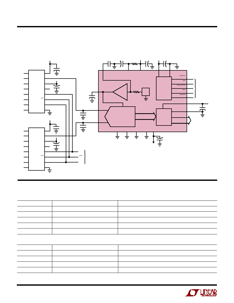
CONVERSION DETAILS
The LTC1604 uses a successive approximation algorithm
and internal sample-and-hold circuit to convert an analog
signal to a 16-bit parallel output. The ADC is complete with
a sample-and-hold, a precision reference and an internal
clock. The control logic provides easy interface to micro-
processors and DSPs. (Please refer to the Digital Interface
section for the data format.)
Conversion start is controlled by the CS and CONVST
inputs. At the start of the conversion the successive
approximation register (SAR) resets. Once a conversion
cycle has begun it cannot be restarted.
During the conversion, the internal differential 16-bit
capacitive DAC output is sequenced by the SAR from the
Most Significant Bit (MSB) to the Least Significant Bit
(LSB). Referring to Figure 1, the A
IN
+
and A
IN
≠
inputs are
acquired during the acquire phase and the comparator
offset is nulled by the zeroing switches. In this acquire
phase, a duration of 480ns will provide enough time for the
sample-and-hold capacitors to acquire the analog signal.
During the convert phase the comparator zeroing switches
open, putting the comparator into compare mode. The
input switches connect the C
SMPL
capacitors to ground,
transferring the differential analog input charge onto the
≠
+
COMP
A
IN
+
C
SMPL
HOLD
SAMPLE
A
IN
≠
C
SMPL
+C
DAC
+V
DAC
≠C
DAC
≠V
DAC
HOLD
HOLD
SAMPLE
HOLD
SAR
OUTPUT
LATCHES
16
D15
D0
1604 F01
∑
∑
∑
ZEROING SWITCHES
Figure 1. Simplified Block Diagram
summing junctions. This input charge is successively
compared with the binary-weighted charges supplied by
the differential capacitive DAC. Bit decisions are made by
the high speed comparator. At the end of a conversion, the
differential DAC output balances the A
IN
+
and A
IN
≠
input
charges. The SAR contents (a 16-bit data word) which
represent the difference of A
IN
+
and A
IN
≠
are loaded into
the 16-bit output latches.
DIGITAL INTERFACE
The A/D converter is designed to interface with micropro-
cessors as a memory mapped device. The CS and RD
control inputs are common to all peripheral memory
interfacing. A separate CONVST is used to initiate a con-
version.
Internal Clock
The A/D converter has an internal clock that runs the A/D
conversion. The internal clock is factory trimmed to achieve
a typical conversion time of 2.45
µ
s and a maximum
conversion time of 2.8
µ
s over the full temperature range.
No external adjustments are required. The guaranteed
maximum acquisition time is 480ns. In addition, a through-
put time (acquisition + conversion) of 3
µ
s and a minimum
sampling rate of 333ksps are guaranteed.
3V Input/Output Compatible
The LTC1604 operates on
±
5V supplies, which makes the
device easy to interface to 5V digital systems. This device
can also talk to 3V digital systems: the digital input pins
(SHDN, CS, CONVST and RD) of the LTC1604 recognize
3V or 5V inputs. The LTC1604 has a dedicated output
supply pin (OV
DD
) that controls the output swings of the
digital output pins (D0 to D15, BUSY) and allows the part
to talk to either 3V or 5V digital systems. The output is
two's complement binary.
Power Shutdown
The LTC1604 provides two power shutdown modes, Nap
and Sleep, to save power during inactive periods. The Nap
mode reduces the power by 95% and leaves only the
digital logic and reference powered up. The wake-up time
from Nap to active is 200ns. In Sleep mode all bias
9
LTC1604
APPLICATIO
N
S I
N
FOR
M
ATIO
N
W
U
U
U
currents are shut down and only leakage current remains
(about 1
µ
A). Wake-up time from Sleep mode is much
slower since the reference circuit must power up and
settle. Sleep mode wake-up time is dependent on the value
of the capacitor connected to the REFCOMP (Pin 4). The
wake-up time is 160ms with the recommended 47
µ
F
capacitor.
Shutdown is controlled by Pin 33 (SHDN). The ADC is in
shutdown when SHDN is low. The shutdown mode is
selected with Pin 32 (CS). When SHDN is low, CS low
selects nap and CS high selects sleep.
Figure 2a. Nap Mode to Sleep Mode Timing
t
3
SHDN
CS
1604 F02a
t
4
SHDN
CONVST
1604 F02b
Figure 2b. SHDN to CONVST Wake-Up Timing
t
2
t
1
CS
CONVST
RD
1604 F03
Figure 3. CS top CONVST Setup Timing
0
CHANGE IN DNL (LSB)
2800
1604 F04
400
800
1600
1200
2000
2400
4
3
2
1
0
CONVST LOW TIME, t
5
(ns)
t
CONV
t
ACQ
Figure 4. Change in DNL vs CONVST Low Time. Be Sure the
CONVST Pulse Returns High Early in the Conversion or After
the End of Conversion
Timing and Control
Conversion start and data read operations are controlled
by three digital inputs: CONVST, CS and RD. A falling edge
applied to the CONVST pin will start a conversion after the
ADC has been selected (i.e., CS is low). Once initiated, it
cannot be restarted until the conversion is complete.
Converter status is indicated by the BUSY output. BUSY is
low during a conversion.
We recommend using a narrow logic low or narrow logic
high CONVST pulse to start a conversion as shown in
Figures 5 and 6. A narrow low or high CONVST pulse
prevents the rising edge of the CONVST pulse from upset-
ting the critical bit decisions during the conversion time.
Figure 4 shows the change of the differential nonlinearity
error versus the low time of the CONVST pulse. As shown,
if CONVST returns high early in the conversion (e.g.,
CONVST low time <500ns), accuracy is unaffected. Simi-
larly, if CONVST returns high after the conversion is over
(e.g., CONVST low time >t
CONV
), accuracy is unaffected.
For best results, keep t
5
less than 500ns or greater than
t
CONV
.
Figures 5 through 9 show several different modes of
operation. In modes 1a and 1b (Figures 5 and 6), CS and
RD are both tied low. The falling edge of CONVST starts the
conversion. The data outputs are always enabled and data
can be latched with the BUSY rising edge. Mode 1a shows
operation with a narrow logic low CONVST pulse. Mode 1b
shows a narrow logic high CONVST pulse.
In mode 2 (Figure 7) CS is tied low. The falling edge of
CONVST signal starts the conversion. Data outputs are in
10
LTC1604
APPLICATIO
N
S I
N
FOR
M
ATIO
N
W
U
U
U
(CONVST = )
Figure 5. Mode 1a. CONVST Starts a Conversion. Data Outputs Always Enabled
DATA N
D15 TO D0
DATA (N + 1)
D15 TO D0
DATA (N ≠ 1)
D15 TO D0
CONVST
CS = RD = 0
BUSY
1604 F05
t
5
t
CONV
t
6
t
8
t
7
DATA
Figure 7. Mode 2. CONVST Starts a Conversion. Data is Read by RD
CONVST
CS = 0
BUSY
1604 F07
t
5
t
CONV
t
8
t
13
t
6
t
9
t
12
DATA N
D15 TO D0
t
11
t
10
RD
DATA
DATA (N ≠ 1)
D15 TO D0
CONVST
BUSY
1604 F06
t
CONV
t
6
t
13
t
7
CS = RD = 0
DATA N
D15 TO D0
DATA (N + 1)
D15 TO D0
DATA
t
5
t
6
t
8
Figure 6. Mode 1b. CONVST Starts a Conversion. Data Outputs Always Enabled
(CONVST = )
11
LTC1604
APPLICATIO
N
S I
N
FOR
M
ATIO
N
W
U
U
U
RD = CONVST
CS = 0
BUSY
1604 F08
t
CONV
t
6
DATA (N ≠ 1)
D5 TO D0
DATA
DATA N
D15 TO D0
DATA (N + 1)
D15 TO D0
DATA N
D15 TO D0
t
11
t
8
t
10
t
7
RD = CONVST
BUSY
CS = 0
1604 F09
t
CONV
t
6
DATA (N ≠ 1)
D15 TO D0
DATA
DATA N
D15 TO D0
t
10
t
11
t
8
Figure 8. Mode 2. Slow Memory Mode Timing
Figure 9. ROM Mode Timing
three-state until read by the MPU with the RD signal. Mode
2 can be used for operation with a shared data bus.
In slow memory and ROM modes (Figures 8 and 9) CS is
tied low and CONVST and RD are tied together. The MPU
starts the conversion and reads the output with the com-
bined CONVST-RD signal. Conversions are started by the
MPU or DSP (no external sample clock is needed).
In slow memory mode the processor applies a logic low to
RD (= CONVST), starting the conversion. BUSY goes low,
forcing the processor into a wait state. The previous
conversion result appears on the data outputs. When the
conversion is complete, the new conversion results
appear on the data outputs; BUSY goes high, releasing the
processor and the processor takes RD (= CONVST) back
high and reads the new conversion data.
In ROM mode, the processor takes RD (= CONVST) low,
starting a conversion and reading the previous conversion
result. After the conversion is complete, the processor can
read the new result and initiate another conversion.
DIFFERENTIAL ANALOG INPUTS
Driving the Analog Inputs
The differential analog inputs of the LTC1604 are easy to
drive. The inputs may be driven differentially or as a single-
ended input (i.e., the A
IN
≠
input is grounded). The A
IN
+
and
A
IN
≠
inputs are sampled at the same instant. Any un-
wanted signal that is common mode to both inputs will be
reduced by the common mode rejection of the sample-
and-hold circuit. The inputs draw only one small current
spike while charging the sample-and-hold capacitors at
the end of conversion. During conversion the analog
inputs draw only a small leakage current. If the source
impedance of the driving circuit is low, then the LTC1604
inputs can be driven directly. As source impedance in-
creases so will acquisition time (see Figure 10). For
minimum acquisition time with high source impedance, a
buffer amplifier should be used. The only requirement is
that the amplifier driving the analog input(s) must settle
after the small current spike before the next conversion
12
LTC1604
APPLICATIO
N
S I
N
FOR
M
ATIO
N
W
U
U
U
starts (settling time must be 200ns for full throughput
rate).
Choosing an Input Amplifier
Choosing an input amplifier is easy if a few requirements
are taken into consideration. First, to limit the magnitude
of the voltage spike seen by the amplifier from charging
the sampling capacitor, choose an amplifier that has a
low output impedance (< 100
) at the closed-loop band-
width frequency. For example, if an amplifier is used in a
gain of +1 and has a unity-gain bandwidth of 50MHz, then
the output impedance at 50MHz should be less than
100
. The second requirement is that the closed-loop
bandwidth must be greater than 15MHz to ensure
adequate small-signal settling for full throughput rate. If
slower op amps are used, more settling time can be
provided by increasing the time between conversions.
The best choice for an op amp to drive the LTC1604 will
depend on the application. Generally applications fall into
two categories: AC applications where dynamic specifi-
cations are most critical and time domain applications
where DC accuracy and settling time are most critical.
The following list is a summary of the op amps that are
suitable for driving the LTC1604. More detailed informa-
tion is available in the Linear Technology databooks, the
LinearView
TM
CD-ROM and on our web site at:
www.linear-tech. com.
Figure 10. t
ACQ
vs Source Resistance
LT
Æ
1007: Low Noise Precision Amplifier. 2.7mA supply
current,
±
5V to
±
15V supplies, gain bandwidth product
8MHz, DC applications.
LT1097: Low Cost, Low Power Precision Amplifier. 300
µ
A
supply current,
±
5V to
±
15V supplies, gain bandwidth
product 0.7MHz, DC applications.
LT1227: 140MHz Video Current Feedback Amplifier. 10mA
supply current,
±
5V to
±
15V supplies, low noise and low
distortion.
LT1360: 37MHz Voltage Feedback Amplifier. 3.8mA sup-
ply current,
±
5V to
±
15V supplies, good AC/DC specs.
LT1363: 50MHz Voltage Feedback Amplifier. 6.3mA sup-
ply current, good AC/DC specs.
LT1364/LT1365: Dual and Quad 50MHz Voltage Feedback
Amplifiers. 6.3mA supply current per amplifier, good AC/
DC specs.
Input Filtering
The noise and the distortion of the input amplifier and
other circuitry must be considered since they will add to
the LTC1604 noise and distortion. The small-signal band-
width of the sample-and-hold circuit is 15MHz. Any noise
or distortion products that are present at the analog inputs
will be summed over this entire bandwidth. Noisy input
circuitry should be filtered prior to the analog inputs to
minimize noise. A simple 1-pole RC filter is sufficient for
many applications. For example, Figure 11 shows a 3000pF
capacitor from A
IN
+
to ground and a 100
source resistor
to limit the input bandwidth to 530kHz. The 3000pF
capacitor also acts as a charge reservoir for the input
sample-and-hold and isolates the ADC input from sam-
pling glitch sensitive circuitry. High quality capacitors and
resistors should be used since these components can add
distortion. NPO and silver mica type dielectric capacitors
have excellent linearity. Carbon surface mount resistors can
also generate distortion from self heating and from damage
that may occur during soldering. Metal film surface mount
resistors are much less susceptible to both problems.
LinearView is a trademark of Linear Technology Corporation.
SOURCE RESISTANCE (
)
1
10
100
1k
10k
ACQUISITION TIME (
µ
s)
10
1
0.1
0.01
1604 F10
13
LTC1604
APPLICATIO
N
S I
N
FOR
M
ATIO
N
W
U
U
U
LTC1604
A
IN
+
A
IN
≠
V
REF
REFCOMP
AGND
1604 F11
1
2
3
4
5
47
µ
F
3000pF
100
ANALOG INPUT
Figure 11. RC Input Filter
Input Range
The
±
2.5V input range of the LTC1604 is optimized for low
noise and low distortion. Most op amps also perform well
over this same range, allowing direct coupling to the
analog inputs and eliminating the need for special transla-
tion circuitry.
Some applications may require other input ranges. The
LTC1604 differential inputs and reference circuitry can
accommodate other input ranges often with little or no
additional circuitry. The following sections describe the
reference and input circuitry and how they affect the input
range.
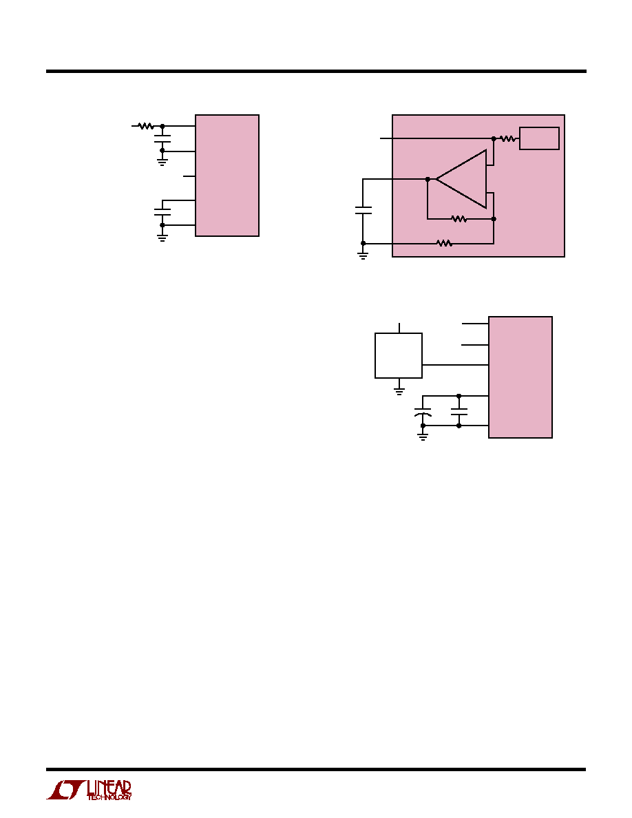
Internal Reference
The LTC1604 has an on-chip, temperature compensated,
curvature corrected, bandgap reference that is factory
trimmed to 2.500V. It is connected internally to a reference
amplifier and is available at V
REF
(Pin 3) (see Figure 12a).
A 7.5k resistor is in series with the output so that it can be
easily overdriven by an external reference or other
circuitry (see Figure 12b). The reference amplifier gains
the voltage at the V
REF
pin by 1.75 to create the required
internal reference voltage. This provides buffering
between the V
REF
pin and the high speed capacitive DAC.
The reference amplifier compensation pin (REFCOMP, Pin
4) must be bypassed with a capacitor to ground. The
reference amplifier is stable with capacitors of 22
µ
F or
greater. For the best noise performance a 47
µ
F ceramic or
47
µ
F tantalum in parallel with a 0.1
µ
F ceramic is recom-
mended.
R2
12k
R3
16k
REFERENCE
AMP
47
µ
F
REFCOMP
AGND
V
REF
R1
7.5k
3
4
5
2.500V
4.375V
LTC1604
1604 F12a
BANDGAP
REFERENCE
Figure 12a. LTC1604 Reference Circuit
1
2
3
0.1
µ
F
10
µ
F
ANALOG
INPUT
1604 F12b
LT1019A-2.5
V
OUT
V
IN
5V
A
IN
+
A
IN
≠
V
REF
LTC1604
AGND
REFCOMP
5
4
+
Figure 12b. Using the LT1019-2.5 as an External Reference
The V
REF
pin can be driven with a DAC or other means
shown in Figure 13. This is useful in applications where the
peak input signal amplitude may vary. The input span of
the ADC can then be adjusted to match the peak input
signal, maximizing the signal-to-noise ratio. The filtering
of the internal LTC1604 reference amplifier will limit
the bandwidth and settling time of this circuit. A settling
time of 20ms should be allowed for after a reference
adjustment.
Differential Inputs
The LTC1604 has a unique differential sample-and-hold
circuit that allows rail-to-rail inputs. The ADC will always
convert the difference of A
IN
+
≠ A
IN
≠
independent of the
common mode voltage (see Figure 15a). The common
mode rejection holds up to extremely high frequencies
(see Figure 14a). The only requirement is that both inputs
14
LTC1604
APPLICATIO
N
S I
N
FOR
M
ATIO
N
W
U
U
U
LTC1604
A
IN
+
ANALOG INPUT
2V TO 2.7V
DIFFERENTIAL
A
IN
≠
V
REF
REFCOMP
AGND
1604 F13
1
2
3
4
5
47
µ
F
LTC1450
2V TO 2.7V
Figure 14a. CMRR vs Input Frequency
INPUT FREQUENCY (Hz)
1k
COMMON MODE REJECTION (dB)
80
70
60
50
40
30
20
10
0
10k
100k
1604 G14a
1M
Figure 13. Driving V
REF
with a DAC
can not exceed the AV
DD
or V
SS
power supply voltages.
Integral nonlinearity errors (INL) and differential nonlin-
earity errors (DNL) are independent of the common mode
voltage, however, the bipolar zero error (BZE) will vary.
The change in BZE is typically less than 0.1% of the
common mode voltage. Dynamic performance is also
affected by the common mode voltage. THD will degrade
as the inputs approach either power supply rail, from 96dB
with a common mode of 0V to 86dB with a common mode
of 2.5V or ≠ 2.5V.
Differential inputs allow greater flexibility for accepting
different input ranges. Figure 14b shows a circuit that
converts a 0V to 5V analog input signal with only an
additional buffer that is not in the signal path.
LTC1604
A
IN
+
A
IN
≠
V
REF
0V TO
5V
±
2.5V
REFCOMP
AGND
1604 F14b
1
2
3
4
5
10
µ
F
ANALOG INPUT
≠
+
Figure 14b. Selectable 0V to 5V or
±
2.5V Input Range
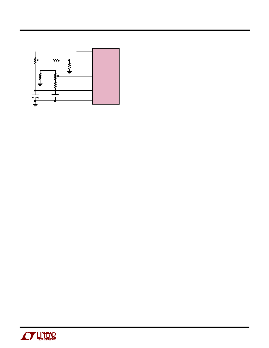
Full-Scale and Offset Adjustment
Figure 15a shows the ideal input/output characteristics
for the LTC1604. The code transitions occur midway
between successive integer LSB values (i.e., ≠ FS +
0.5LSB, ≠ FS + 1.5LSB, ≠ FS + 2.5LSB,... FS ≠ 1.5LSB,
FS ≠ 0.5LSB). The output is two's complement binary with
1LSB = FS ≠ (≠ FS)/65536 = 5V/65536 = 76.3
µ
V.
In applications where absolute accuracy is important,
offset and full-scale errors can be adjusted to zero. Offset
error must be adjusted before full-scale error. Figure 15b
shows the extra components required for full-scale error
adjustment. Zero offset is achieved by adjusting the offset
applied to the A
IN
≠
input. For zero offset error apply
1604 F15a
011...111
011...110
000...001
000...000
111...111
111...110
100...001
100...000
FS ≠ 1LSB
≠ (FS ≠ 1LSB)
INPUT VOLTAGE (A
IN
+
≠ A
IN
≠
)
OUTPUT CODE
Figure 15a. LTC1604 Transfer Characteristics
15
LTC1604
analog ground plane. No other digital grounds should be
connected to this analog ground plane. Low impedance
analog and digital power supply common returns are
essential to low noise operation of the ADC and the foil
width for these tracks should be as wide as possible. In
applications where the ADC data outputs and control
signals are connected to a continuously active micropro-
cessor bus, it is possible to get errors in the conversion
results. These errors are due to feedthrough from the
microprocessor to the successive approximation com-
parator. The problem can be eliminated by forcing the
microprocessor into a WAIT state during conversion or by
using three-state buffers to isolate the ADC data bus. The
traces connecting the pins and bypass capacitors must be
kept short and should be made as wide as possible.
The LTC1604 has differential inputs to minimize noise
coupling. Common mode noise on the A
IN
+
and A
IN
≠
leads
will be rejected by the input CMRR. The A
IN
≠
input can be
used as a ground sense for the A
IN
+
input; the LTC1604
will hold and convert the difference voltage between A
IN
+
and A
IN
≠
. The leads to A
IN
+
(Pin 1) and A
IN
≠
(Pin 2) should
be kept as short as possible. In applications where this is
not possible, the A
IN
+
and A
IN
≠
traces should be run side
by side to equalize coupling.
SUPPLY BYPASSING
High quality, low series resistance ceramic, 10
µ
F or 47
µ
F
bypass capacitors should be used at the V
DD
and REFCOMP
pins as shown in Figure 16 and in the Typical Application
on the first page of this data sheet. Surface mount ceramic
capacitors such as Murata GRM235Y5V106Z016 provide
excellent bypassing in a small board space. Alternatively,
10
µ
F tantalum capacitors in parallel with 0.1
µ
F ceramic
capacitors can be used. Bypass capacitors must be lo-
cated as close to the pins as possible. The traces connect-
ing the pins and the bypass capacitors must be kept short
and should be made as wide as possible.
APPLICATIO
N
S I
N
FOR
M
ATIO
N
W
U
U
U
ANALOG
INPUT
1604 F15b
1
2
3
R4
100
R7
50k
R3
24k
≠5V
R6
24k
R8
50k
R5
47k
4
5
0.1
µ
F
47
µ
F
+
A
IN
+
A
IN
≠
V
REF
REFCOMP
AGND
LTC1604
Figure 15b. Offset and Full-Scale Adjust Circuit
≠ 38
µ
V (i.e., ≠ 0.5LSB) at A
IN
+
and adjust the offset at the
A
IN
≠
input until the output code flickers between 0000
0000 0000 0000 and 1111 1111 1111 1111. For full-scale
adjustment, an input voltage of 2.499886V (FS/2 ≠ 1.5LSBs)
is applied to A
IN
+
and R2 is adjusted until the output code
flickers between 0111 1111 1111 1110 and 0111 1111
1111 1111.
BOARD LAYOUT AND GROUNDING
Wire wrap boards are not recommended for high resolu-
tion or high speed A/D converters. To obtain the best
performance from the LTC1604, a printed circuit board
with ground plane is required. Layout should ensure that
digital and analog signal lines are separated as much as
possible. Particular care should be taken not to run any
digital track alongside an analog signal track or under-
neath the ADC.The analog input should be screened by
AGND.
An analog ground plane separate from the logic system
ground should be established under and around the ADC.
Pin 5 to Pin 8 (AGNDs), Pin 10 (ADC's DGND) and all other
analog grounds should be connected to this single analog
ground point. The REFCOMP bypass capacitor and the
DV
DD
bypass capacitor should also be connected to this
16
LTC1604
APPLICATIO
N
S I
N
FOR
M
ATIO
N
W
U
U
U
1604 F16
A
IN
+
V
SS
OV
DD
DGND
AV
DD
LTC1604
DIGITAL
SYSTEM
ANALOG
INPUT
CIRCUITRY
AGND
5 TO 8
2
34
29
DV
DD
OGND
28
10
1
REFCOMP
4
47
µ
F
V
REF
3
2.2
µ
F
A
IN
≠
10
µ
F
36
10
µ
F
AV
DD
35
10
µ
F
10
µ
F
+
≠
9
10
µ
F
DC PERFORMANCE
The noise of an ADC can be evaluated in two ways: signal-
to-noise raio (SNR) in frequency domain and histogram in
time domain. The LTC1604 excels in both. Figure 18a
demonstrates that the LTC1604 has an SNR of over 90dB
in frequency domain. The noise in the time domain histo-
gram is the transition noise associated with a high resolu-
tion ADC which can be measured with a fixed DC signal
applied to the input of the ADC. The resulting output codes
are collected over a large number of conversions. The
shape of the distribution of codes will give an indication of
the magnitude of the transition noise. In Figure 17 the
distribution of output codes is shown for a DC input that
has been digitized 4096 times. The distribution is Gaussian
and the RMS code transition noise is about 0.66LSB. This
corresponds to a noise level of 90.9dB relative to full scale.
Adding to that the theoretical 98dB of quantization error
for 16-bit ADC, the resultant corresponds to an SNR level
of 90.1dB which correlates very well to the frequency
domain measurements in DYNAMIC PERFORMANCE
section.
DYNAMIC PERFORMANCE
The LTC1604 has excellent high speed sampling capabil-
ity. Fast fourier transform (FFT) test techniques are used
to test the ADC's frequency response, distortions and
noise at the rated throughput. By applying a low distortion
sine wave and analyzing the digital output using an FFT
algorithm, the ADC's spectral content can be examined for
frequencies outside the fundamental. Figures 18a and 18b
show typical LTC1604 FFT plots.
CODE
≠5 ≠4 ≠3 ≠2 ≠1 0
1
2
3
4
5
COUNT
2500
2000
1500
1000
500
0
1604 F17
Figure 17. Histogram for 4096 Conversions
FREQUENCY (kHz)
0
AMPLITUDE (dB)
≠60
≠40
≠20
60
1604 F18a
≠80
≠100
20
40
80 100 120 140 160
≠120
≠140
0
f
SAMPLE
= 333kHz
f
IN
= 4.959kHz
SINAD = 90.2dB
THD = ≠103.2dB
Figure 18a. This FFT of the LTC1604's Conversion of a
Full-Scale 5kHz Sine Wave Shows Outstanding Response
with a Very Low Noise Floor When Sampling at 333ksps
Figure 16. Power Supply Grounding Practice
17
LTC1604
APPLICATIO
N
S I
N
FOR
M
ATIO
N
W
U
U
U
Signal-to-Noise Ratio
The signal-to-noise plus distortion ratio [S/(N + D)] is the
ratio between the RMS amplitude of the fundamental input
frequency to the RMS amplitude of all other frequency
components at the A/D output. The output is band limited
to frequencies from above DC and below half the sampling
frequency. Figure 18a shows a typical spectral content
with a 333kHz sampling rate and a 5kHz input. The
dynamic performance is excellent for input frequencies up
to and beyond the Nyquist limit of 167kHz.
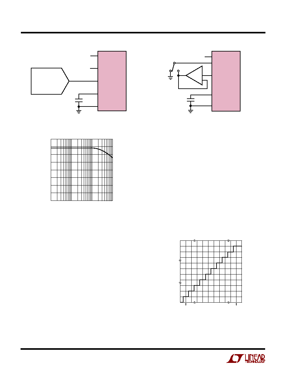
Effective Number of Bits
The effective number of bits (ENOBs) is a measurement of
the resolution of an ADC and is directly related to the
S/(N + D) by the equation:
N = [S/(N + D) ≠ 1.76]/6.02
where N is the effective number of bits of resolution and
S/(N + D) is expressed in dB. At the maximum sampling
rate of 333kHz the LTC1604 maintains above 14 bits up to
the Nyquist input frequency of 167kHz (refer to Figure 19).
Total Harmonic Distortion
Total harmonic distortion (THD) is the ratio of the RMS
sum of all harmonics of the input signal to the fundamental
itself. The out-of-band harmonics alias into the frequency
band between DC and half the sampling frequency. THD is
expressed as:
THD
Log
V
V
V
Vn
V
=
+
+
+
20
2
3
4
1
2
2
2
2
...
where V1 is the RMS amplitude of the fundamental fre-
quency and V2 through Vn are the amplitudes of the
second through nth harmonics. THD vs Input Frequency is
shown in Figure 20. The LTC1604 has good distortion
performance up to the Nyquist frequency and beyond.
FREQUENCY (kHz)
AMPLITUDE (dB)
≠60
≠40
≠20
1604 F18b
≠80
≠100
≠120
≠140
0
0
60
20
40
80 100 120 140 160
f
SAMPLE
= 333kHz
f
IN
= 97.152kHz
SINAD = 89dB
THD = ≠96dB
FREQUENCY (Hz)
1k
EFFECTIVE BITS
SINAD (dB)
16
15
14
13
12
11
10
9
8
98
92
86
80
74
68
62
56
50
10k
100k
1M
1604 F19
Figure 18b. Even with Inputs at 100kHz, the LTC1604's
Dynamic Linearity Remains Robust
INPUT FREQUENCY (Hz)
0
≠10
≠20
≠30
≠40
≠50
≠60
≠70
≠80
≠90
≠100
≠110
AMPLITUDE (dB BELOW THE FUNDAMENTAL)
1604 G04
1k
10k
100k
1M
THD
3RD
2ND
Figure 20. Distortion vs Input Frequency
Figure 19. Effective Bits and Signal/(Noise + Distortion)
vs Input Frequency
18
LTC1604
Intermodulation Distortion
If the ADC input signal consists of more than one spectral
component, the ADC transfer function nonlinearity can
produce intermodulation distortion (IMD) in addition to
THD. IMD is the change in one sinusoidal input caused by
the presence of another sinusoidal input at a different
frequency.
If two pure sine waves of frequencies fa and fb are applied
to the ADC input, nonlinearities in the ADC transfer func-
tion can create distortion products at the sum and differ-
ence frequencies of mfa
±
nfb, where m and n = 0, 1, 2, 3,
APPLICATIO
N
S I
N
FOR
M
ATIO
N
W
U
U
U
etc. For example, the 2nd order IMD terms include
(fa ≠ fb). If the two input sine waves are equal in magni-
tude, the value (in decibels) of the 2nd order IMD products
can be expressed by the following formula:
IMD fa
fb
Log
Amplitude
±
( )
=
±
20
at (fa
fb)
Amplitude at fa
Peak Harmonic or Spurious Noise
The peak harmonic or spurious noise is the largest spec-
tral component excluding the input signal and DC. This
value is expressed in decibels relative to the RMS value of
a full-scale input signal.
Full-Power and Full-Linear Bandwidth
The full-power bandwidth is that input frequency at which
the amplitude of the reconstructed fundamental is
reduced by 3dB for a full-scale input signal.
The full-linear bandwidth is the input frequency at which
the S/(N + D) has dropped to 84dB (13.66 effective bits).
The LTC1604 has been designed to optimize input band-
width, allowing the ADC to undersample input signals with
frequencies above the converter's Nyquist Frequency. The
noise floor stays very low at high frequencies; S/(N + D)
becomes dominated by distortion at frequencies far
beyond Nyquist.
FREQUENCY (kHz)
0
20
AMPLITUDE (dB)
80
100
0
≠20
≠40
≠60
≠80
≠100
≠120
≠140
1604 G06
40
60
160
120 140
f
SAMPLE
= 333kHz
f
IN1
= 29.3kHz
f
IN2
= 32.4kHz
Figure 21. Intermodulation Distortion Plot
19
LTC1604
Information furnished by Linear Technology Corporation is believed to be accurate and reliable.
However, no responsibility is assumed for its use. Linear Technology Corporation makes no represen-
tation that the interconnection of its circuits as described herein will not infringe on existing patent rights.
Dimensions in inches (millimeters) unless otherwise noted.
PACKAGE DESCRIPTIO
N
U
G Package
36-Lead Plastic SSOP (0.209)
(LTC DWG # 05-08-1640)
G36 SSOP 1196
0.005 ≠ 0.009
(0.13 ≠ 0.22)
0
∞
≠ 8
∞
0.022 ≠ 0.037
(0.55 ≠ 0.95)
0.205 ≠ 0.212**
(5.20 ≠ 5.38)
0.301 ≠ 0.311
(7.65 ≠ 7.90)
1 2 3 4 5 6 7 8 9 10 11 12
14 15 16 17 18
13
0.499 ≠ 0.509*
(12.67 ≠ 12.93)
25
26
22 21 20 19
23
24
27
28
29
30
31
32
33
34
35
36
0.068 ≠ 0.078
(1.73 ≠ 1.99)
0.002 ≠ 0.008
(0.05 ≠ 0.21)
0.0256
(0.65)
BSC
0.010 ≠ 0.015
(0.25 ≠ 0.38)
DIMENSIONS DO NOT INCLUDE MOLD FLASH. MOLD FLASH
SHALL NOT EXCEED 0.006" (0.152mm) PER SIDE
DIMENSIONS DO NOT INCLUDE INTERLEAD FLASH. INTERLEAD
FLASH SHALL NOT EXCEED 0.010" (0.254mm) PER SIDE
*
**
20
LTC1604
1604fa LT/TP 1098 REV A 2K ∑ PRINTED IN USA
©
LINEAR TECHNOLOGY CORPORATION 1998
TYPICAL APPLICATIO
N
U
Linear Technology Corporation
1630 McCarthy Blvd., Milpitas, CA 95035-7417
(408) 432-1900
q
FAX: (408) 434-0507
q
www.linear-tech.com
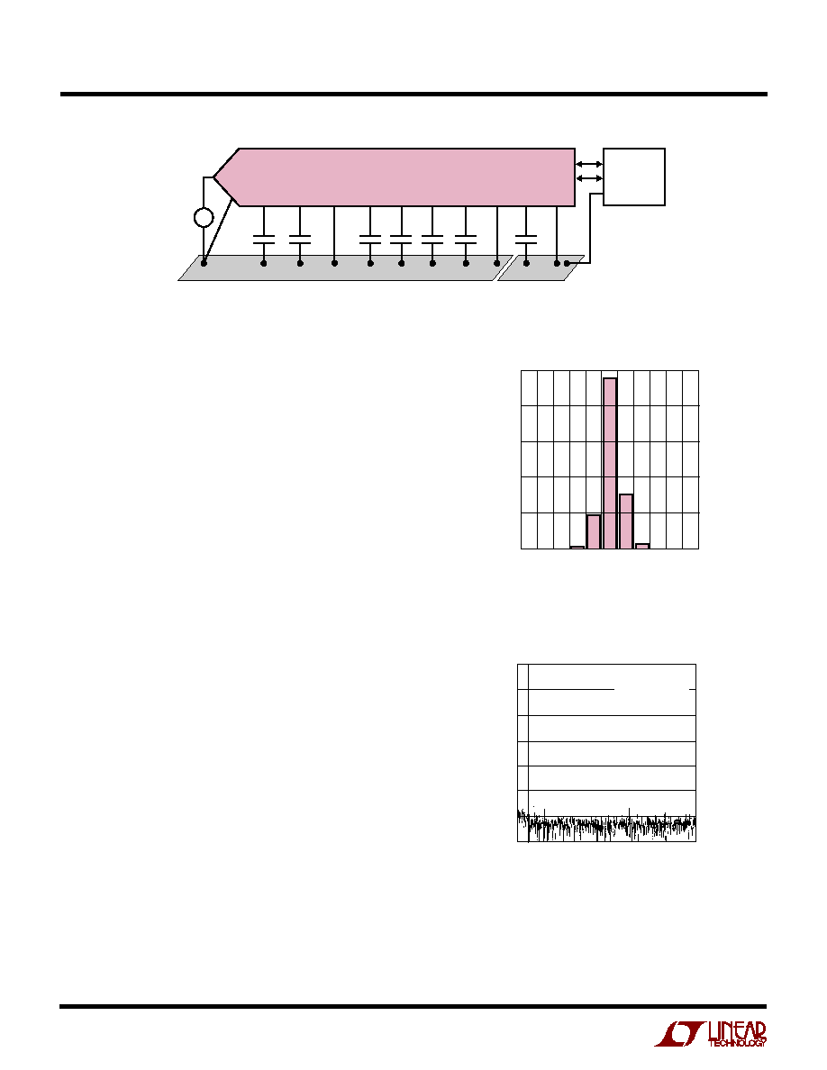
Using the LTC1604 and Two LTC1391s as an 8-Channel Differential 16-Bit ADC System
D15 TO D0
V
SS
AGND
AGND
AGND
AGND
REFCOMP
4.375V
11 TO 26
1604 TA03
CH7
+
+
+
+
CH0
+
16
15
14
13
12
11
10
9
1
2
3
4
5
6
7
8
LTC1391
LTC1391
CH0
CH1
CH2
CH3
CH4
CH5
CH6
CH7
V
+
D
V
≠
D
OUT
D
IN
CS
CLK
GND
CH7
≠
CH0
≠
1
µ
F
5V
D
IN
CS
CLK
≠5V
≠5V
10
2.2
µ
F
10
µ
F
5V
10
µ
F
5V
10
34
9
35
36
3
4
10
µ
F
≠5V
1
µ
F
10
µ
F
3000pF
3000pF
5
1
47
µ
F
A
IN
+
V
REF
AV
DD
AV
DD
DV
DD
DGND
OV
DD
OGND 28
µ
P
CONTROL
LINES
5V OR
3V
10
µ
F
SHDN
CS
CONVST
RD
BUSY
33
32
31
30
27
A
IN
≠
2
6
7
8
1
µ
F
5V
16
15
14
13
12
11
10
9
1
2
3
4
5
6
7
8
CH0
CH1
CH2
CH3
CH4
CH5
CH6
CH7
V
+
D
V
≠
D
OUT
D
IN
CS
CLK
GND
16-BIT
SAMPLING
ADC
+
+
+
+
+
1.75X
2.5V
REF
CONTROL
LOGIC
AND
TIMING
OUTPUT
BUFFERS
16-BIT
PARALLEL
BUS
7.5k
LTC1604
B15 TO B0
+
29
µ
P
CONTROL
LINES
+
≠
RELATED PARTS
PART NUMBER
DESCRIPTION
COMMENTS
LTC1410
12-Bit, 1.25Msps,
±
5V ADC
71.5dB SINAD at Nyquist, 150mW Dissipation
LTC1415
12-Bit, 1.25Msps, Single 5V ADC
55mW Power Dissipation, 72dB SINAD
LTC1418
14-Bit, 200ksps, Single 5V ADC
15mW, Serial/Para llel
±
10V
LTC1419
Low Power 14-Bit, 800ksps ADC
True 14-Bit Linearity, 81.5dB SINAD, 150mW Dissipation
LTC1605
16-Bit, 100ksps, Single 5V ADC
±
10V Inputs, 55mW, Byte or Parallel I/O
SAMPLING ADCs
DACs
PART NUMBER
DESCRIPTION
COMMENTS
LTC1595
16-Bit Serial Multiplying I
OUT
DAC in SO-8
±
1LSB Max INL/DNL, Low Glitch, DAC8043 16-Bit Upgrade
LTC1596
16-Bit Serial Multiplying I
OUT
DAC
±
1LSB Max INL/DNL, Low Glitch, AD7543/DAC8143 16-Bit Upgrade
LTC1597
16-Bit Parallel, Multiplying DAC
±
1LSB Max INL/DNL, Low Glitch, 4 Quadrant Resistors
LTC1650
16-Bit Serial V
OUT
DAC
Low Power, Low Gritch, 4-Quadrant Multiplication