1
LTC1605-1/LTC1605-2
Single Supply 16-Bit, 100ksps,
Sampling ADCs
The LTC
Æ
1605-1/LTC1605-2 are 100ksps, sampling
16-bit A/D converters that draw only 55mW (typical) from
a single 5V supply. These easy-to-use devices include a
sample-and-hold, precision reference, switched capacitor
successive approximation A/D and trimmed internal clock.
The LTC1605-1's input range is 0V to 4V while the
LTC1605-2's input range is
±
4V. An external reference
can be used if greater accuracy over temperature is
needed.
The ADC has a microprocessor compatible, 16-bit or two
byte parallel output port. A convert start input and a data
ready signal (BUSY) ease connections to FIFOs, DSPs and
microprocessors.
s
Sample Rate: 100ksps
s
Complete 16-Bit Solution on a Single 5V Supply
s
Unipolar Input Range: 0V to 4V (LTC1605-1)
s
Bipolar Input Range:
±
4V (LTC1605-2)
s
Power Dissipation: 55mW Typ
s
Signal-to-Noise Ratio: 86dB Typ
s
Operates with Internal or External Reference
s
Internal Synchronized Clock
s
28-Pin 0.3" PDIP and SSOP Packages
, LTC and LT are registered trademarks of Linear Technology Corporation.
s
Industrial Process Control
s
Multiplexed Data Acquisition Systems
s
High Speed Data Acquisition for PCs
s
Digital Signal Processing
LTC1605-1 Low Power, 100kHz, 16-Bit Sampling ADC on 5V Supply
4k
4k
200
2.5V
REFERENCE
20k
10k
16-BIT
SAMPLING ADC
D15 TO D0
33.2k
2.2
µ
F
2.5V
2.5V
10
µ
F
0.1
µ
F
2.2
µ
F
0V TO 4V
INPUT
V
IN
CAP
REF
AGND1
1
4
2
AGND2
5
DGND
14
CONTROL
LOGIC AND
TIMING
BUSY
BYTE
CS
R/C
28
27
6 TO 13
15 TO 22
26
25
24
23
DIGITAL
CONTROL
SIGNALS
1605-1/2 TA01
16-BIT
OR 2 BYTE
PARALLEL
BUS
5V
V
DIG
V
ANA
BUFFER
3
CODE
0
INL (LSBs)
65535
1605-1/2 TA02/G04
16384
32768
49152
2.0
1.5
1.0
0.5
0
≠0.5
≠1.0
≠1.5
≠2.0
Typical INL Curve
FEATURES
DESCRIPTIO
U
APPLICATIO S
U
TYPICAL APPLICATIO
U
2
LTC1605-1/LTC1605-2
(Notes 1, 2)
V
ANA
.......................................................................... 7V
V
DIG
to V
ANA
........................................................... 0.3V
V
DIG
........................................................................... 7V
Ground Voltage Difference
DGND, AGND1 and AGND2 ..............................
±
0.3V
Analog Inputs (Note 3)
V
IN
.....................................................................
±
25V
CAP ............................ V
ANA
+ 0.3V to AGND2 ≠ 0.3V
REF .................................... Indefinite Short to AGND2
Momentary Short to V
ANA
Digital Input Voltage (Note 4) ........ V
DGND
≠ 0.3V to 10V
Digital Output Voltage ........ V
DGND
≠ 0.3V to V
DIG
+ 0.3V
Power Dissipation .............................................. 500mW
Operating Ambient Temperature Range
LTC1605-1C/LTC1605-2C ....................... 0
∞
C to 70
∞
C
LTC1605-1I/LTC1605-2I .................... ≠ 40
∞
C to 85
∞
C
Storage Temperature Range ................. ≠ 65
∞
C to 150
∞
C
Lead Temperature (Soldering, 10 sec).................. 300
∞
C
Consult factory for Military grade parts.
ORDER PART
NUMBER
LTC1605-1CG
LTC1605-1IG
LTC1605-2CG
LTC1605-2IG
LTC1605-1CN
LTC1605-1IN
LTC1605-2CN
LTC1605-2IN
T
JMAX
= 125
∞
C,
JA
= 95
∞
C/W (G)
T
JMAX
= 125
∞
C,
JA
= 130
∞
C/W (N)
SYMBOL
PARAMETER
CONDITIONS
MIN
TYP
MAX
UNITS
V
IN
Analog Input Range (Note 9)
4.75V
V
ANA
5.25V, 4.75V
V
DIG
5.25V
LTC1605-1
q
0 to 4
V
LTC1605-2
q
±
4
V
C
IN
Analog Input Capacitance
10
pF
R
IN
Analog Input Impedance
10
k
The
q
denotes the specifications which apply over the full operating temperature range, otherwise
PARAMETER
CONDITIONS
MIN
TYP
MAX
UNITS
Resolution
q
16
Bits
No Missing Codes
q
15
Bits
Transition Noise
1
LSB
RMS
Integral Linearity Error
(Note 7)
q
±
3
LSB
Zero Error
Ext. Reference = 2.5V (Note 8)
q
±
10
mV
Zero Error Drift
±
2
ppm/
∞
C
Full-Scale Error Drift
±
7
ppm/
∞
C
Full-Scale Error
Ext. Reference = 2.5V (Notes 12, 13)
q
±
0.50
%
Full-Scale Error Drift
Ext. Reference = 2.5V
±
2
ppm/
∞
C
Power Supply Sensitivity
V
ANA
= V
DIG
= V
DD
V
DD
= 5V
±
5% (Note 9)
±
8
LSB
The
q
denotes the specifications which apply over the full operating
CO VERTER CHARACTERISTICS
U
A ALOG I PUT
U
U
ABSOLUTE AXI U
RATI GS
W
W
W
U
PACKAGE/ORDER I FOR ATIO
U
U
W
1
2
3
4
5
6
7
8
9
10
11
12
13
14
28
27
26
25
24
23
22
21
20
19
18
17
16
15
V
IN
AGND1
REF
CAP
AGND2
D15 (MSB)
D14
D13
D12
D11
D10
D9
D8
DGND
V
DIG
V
ANA
BUSY
CS
R/C
BYTE
D0
D1
D2
D3
D4
D5
D6
D7
G PACKAGE
28-LEAD PLASTIC SSOP
N PACKAGE
28-LEAD PDIP
TOP VIEW
temperature range, otherwise specifications are at T
A
= 25
∞
C. With external reference (Notes 5, 6).
specifications are at T
A
= 25
∞
C. (Note 5)
3
LTC1605-1/LTC1605-2
SYMBOL
PARAMETER
CONDITIONS
MIN
TYP
MAX
UNITS
S/(N + D)
Signal-to-(Noise + Distortion) Ratio
1kHz Input Signal (Note 14)
87
dB
10kHz Input Signal
85
dB
20kHz, ≠ 60dB Input Signal
30
dB
THD
Total Harmonic Distortion
1kHz Input Signal, First 5 Harmonics
≠ 101
dB
10kHz Input Signal, First 5 Harmonics
≠ 92
dB
Peak Harmonic or Spurious Noise
1kHz Input Signal
≠ 101
dB
10kHz Input Signal
≠ 92
dB
Full-Power Bandwidth
(Note 15)
275
kHz
Aperture Delay
40
ns
Aperture Jitter
Sufficient to Meet AC Specs
Transient Response
Full-Scale Step (Note 9)
2
µ
s
Overvoltage Recovery
(Note 16)
150
ns
The
q
denotes the specifications which apply over the full operating temperature range,
PARAMETER
CONDITIONS
MIN
TYP
MAX
UNITS
V
REF
Output Voltage
I
OUT
= 0
q
2.470
2.500
2.520
V
V
REF
Output Tempco
I
OUT
= 0
±
5
ppm/
∞
C
Internal Reference Source Current
1
µ
A
External Reference Voltage for Specified Linearity
(Notes 9, 10)
2.30
2.50
2.70
V
External Reference Current Drain
Ext. Reference = 2.5V (Note 9)
q
100
µ
A
CAP Output Voltage
I
OUT
= 0
2.50
V
SYMBOL
PARAMETER
CONDITIONS
MIN
TYP
MAX
UNITS
V
IH
High Level Input Voltage
V
DD
= 5.25V
q
2.4
V
V
IL
Low Level Input Voltage
V
DD
= 4.75V
q
0.8
V
I
IN
Digital Input Current
V
IN
= 0V to V
DD
q
±
10
µ
A
C
IN
Digital Input Capacitance
5
pF
V
OH
High Level Output Voltage
V
DD
= 4.75V
I
O
= ≠10
µ
A
4.5
V
I
O
= ≠ 200
µ
A
q
4.0
V
V
OL
Low Level Output Voltage
V
DD
= 4.75V
I
O
= 160
µ
A
0.05
V
I
O
= 1.6mA
q
0.10
0.4
V
I
OZ
Hi-Z Output Leakage D15 to D0
V
OUT
= 0V to V
DD
, CS High
q
±
10
µ
A
C
OZ
Hi-Z Output Capacitance D15 to D0
CS High (Note 9)
q
15
pF
I
SOURCE
Output Source Current
V
OUT
= 0V
≠10
mA
I
SINK
Output Sink Current
V
OUT
= V
DD
10
mA
The
q
denotes the specifications which apply over the
The
q
denotes the specifications which apply over the
DY
A
IC ACCURACY
U
W
I TER AL REFERE CE CHARACTERISTICS
U
U
U
DIGITAL I PUTS A D DIGITAL OUTPUTS
U
U
otherwise specifications are at T
A
= 25
∞
C. (Notes 5, 14)
full operating temperature range, otherwise specifications are at T
A
= 25
∞
C. (Note 5)
full operating temperature range, otherwise specifications are at T
A
= 25
∞
C. (Note 5)
4
LTC1605-1/LTC1605-2
The
q
denotes the specifications which apply over the full operating temperature
SYMBOL
PARAMETER
CONDITIONS
MIN
TYP
MAX
UNITS
f
SAMPLE(MAX)
Maximum Sampling Frequency
q
100
kHz
t
CONV
Conversion Time
q
8
µ
s
t
ACQ
Acquisition Time
q
2
µ
s
t
1
Convert Pulse Width
(Note 11)
q
40
ns
t
2
Data Valid Delay After R/C
(Note 9)
q
8
µ
s
t
3
BUSY Delay from R/C
C
L
= 50pF
q
65
ns
t
4
BUSY Low
8
µ
s
t
5
BUSY Delay After End of Conversion
220
ns
t
6
Aperture Delay
40
ns
t
7
Bus Relinquish Time
q
10
35
83
ns
t
8
BUSY Delay After Data Valid
q
50
200
ns
t
9
Previous Data Valid After R/C
7.4
µ
s
t
10
R/C to CS Setup Time
(Notes 9, 10)
10
ns
t
11
Time Between Conversions
10
µ
s
t
12
Bus Access and Byte Delay
(Notes 9, 10)
10
83
ns
The
q
denotes the specifications which apply over the full operating temperature
SYMBOL
PARAMETER
CONDITIONS
MIN
TYP
MAX
UNITS
V
DD
Positive Supply Voltage
(Notes 9, 10)
4.75
5.25
V
I
DD
Positive Supply Current
q
11
16
mA
P
DIS
Power Dissipation
55
80
mW
Note 1: Absolute Maximum Ratings are those values beyond which the life
of a device may be impaired.
Note 2: All voltage values are with respect to ground with DGND, AGND1
and AGND2 wired together (unless otherwise noted).
Note 3: When these pin voltages are taken below ground or above V
ANA
=
V
DIG
= V
DD
, they will be clamped by internal diodes. This product can
handle input currents of greater than 100mA below ground or above V
DD
without latch-up.
Note 4: When these pin voltages are taken below ground, they will be
clamped by internal diodes. This product can handle input currents of
90mA below ground without latchup. These pins are not clamped to V
DD
.
Note 5: V
DD
= 5V, f
SAMPLE
= 100kHz, t
r
= t
f
= 5ns unless otherwise
specified.
Note 6: Linearity, offset and full-scale specifications apply for a V
IN
input
with respect to ground.
Note 7: Integral nonlinearity is defined as the deviation of a code from a
straight line passing through the actual end points of the transfer curve.
The deviation is measured from the center of the quantization band.
Note 8: Zero error for the LTC1605-1 is the voltage measured from
0.5LSB when the output code flickers between 0000 0000 0000 0000
and 0000 0000 0000 0001. Zero error for the LTC1605-2 is the voltage
measured from ≠ 0.5LSB when the output code flickers between 0000
0000 0000 0000 and 1111 1111 1111 1111.
Note 9: Guaranteed by design, not subject to test.
Note 10: Recommended operating conditions.
Note 11: With CS low the falling R/C edge starts a conversion. If R/C
returns high at a critical point during the conversion it can create small
errors. For best results ensure that R/C returns high within 3
µ
s after the
start of the conversion.
Note 12: As measured with fixed resistors shown in Figure 4. Adjustable to
zero with external potentiometer.
Note 13: Full-scale error is the untrimmed deviation from ideal last code
transition, divided by the full-scale range and includes the effect of offset
error.
Note 14: All specifications in dB are referred to a full-scale 4V input for the
LTC1605-1 and to
±
4V input for the LTC1605-2.
Note 15: Full-power bandwidth is defined as full-scale input frequency at
which a signal-to-(noise + distortion) degrades to 60dB or 10 bits of
accuracy.
Note 16: Recovers to specified performance after (
±
20V) input
overvoltage for the LTC1605-1 and
±
15V for the LTC1605-2.
TI I G CHARACTERISTICS
W
U
POWER REQUIRE E TS
W
U
range, otherwise specifications are at T
A
= 25
∞
C. (Note 5)
range, otherwise specifications are at T
A
= 25
∞
C. (Note 5)
5
LTC1605-1/LTC1605-2
TYPICAL PERFOR A CE CHARACTERISTICS
U
W
SUPPLY VOLTAGE (V)
4.50
9.5
SUPPLY CURRENT (mA)
10.0
10.5
11.0
11.5
12.0
12.5
4.75
5.00
5.25
5.50
1605-1/2 G01
f
SAMPLE
= 100kHz
TEMPERATURE (
∞
C)
≠50
10.0
POWER SUPPLY CURRENT (mA)
10.5
11.0
11.5
12.0
≠25
0
25
50
1605-1/2 G02
75
100
f
SAMPLE
= 100kHz
LOAD CURRENT (mA)
CHANGE IN CAP VOLTAGE (V)
0.04
0.02
0
≠0.02
≠0.04
≠0.06
≠0.08
≠0.10
≠60
≠40
≠20
0
1605-1/2 G03
≠70
≠80
≠50
≠30
≠10
10
LTC1605-1
LTC1605-2
CODE
0
DNL (LSB)
65535
1605-1/2 G05
16384
32768
49152
2.0
1.5
1.0
0.5
0
≠0.5
≠1.0
≠1.5
≠2.0
FREQUENCY (kHz)
0
MAGNITUDE (dB)
1605-1/2 G07/F11
5
10 15 20 25 30 35 40 45 50
0
≠10
≠20
≠30
≠40
≠50
≠60
≠70
≠80
≠90
≠100
≠110
≠120
≠130
f
SAMPLE
= 100kHz
f
IN
= 1kHz
SINAD = 87dB
THD = 101.1dB
SNR = 87.2dB
INPUT FREQUENCY (kHz)
1
SINAD (dB)
90
88
86
84
82
80
10
100
1605-1/2 G08
INPUT FREQUENCY (kHz)
1
TOTAL HARMONIC DISTORTION (dB)
≠70
≠80
≠90
≠100
≠110
10
100
1605-1/2 G09
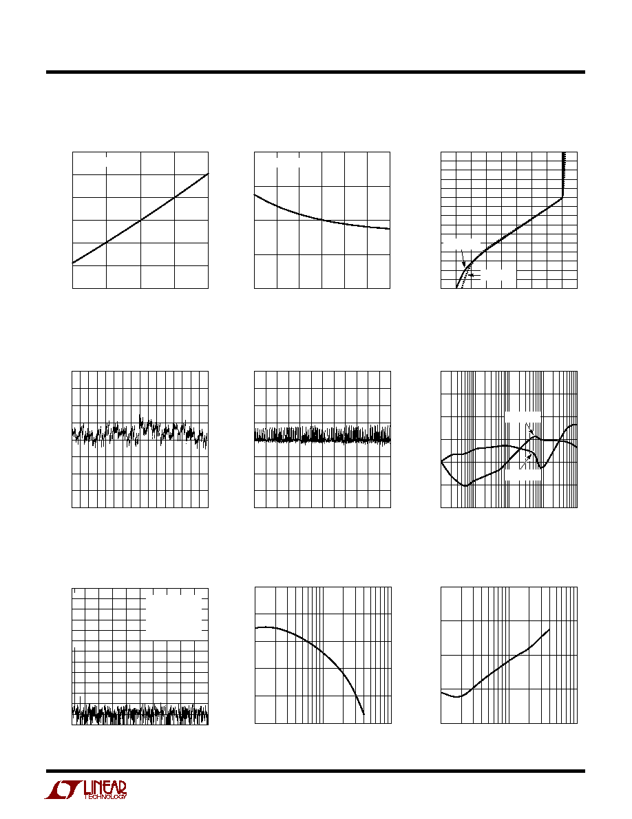
Supply Current vs Supply Voltage
Supply Current vs Temperature
Change in CAP Voltage vs
Load Current
Typical INL Curve
Typical DNL Curve
Power Supply Feedthrough
vs Ripple Frequency
LTC1605-2 Nonaveraged
4096-Point FFT Plot
SINAD vs Input Frequency
(LTC1605-2)
Total Harmonic Distortion vs
Input Frequency (LTC1605-2)
CODE
0
INL (LSBs)
65535
1605-1/2 TA02/G04
16384
32768
49152
2.0
1.5
1.0
0.5
0
≠0.5
≠1.0
≠1.5
≠2.0
RIPPLE FREQUENCY (Hz)
POWER SUPPLY FEEDTHROUGH (dB)
≠20
≠30
≠40
≠50
≠60
≠70
≠80
100
10k
100k
1M
LTXXXX GXX
1k
LTC1605-2
LTC1605-1
6
LTC1605-1/LTC1605-2
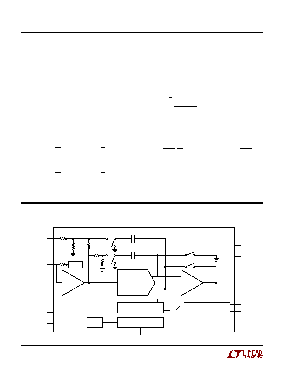
16-BIT CAPACITIVE DAC
COMP
REF BUF
2.5V REF
CAP
(2.5V)
C
SAMPLE
C
SAMPLE
∑
∑
∑
D15
D0
BUSY
CONTROL LOGIC
R/C
BYTE
INTERNAL
CLOCK
CS
ZEROING SWITCHES
V
DIG
V
ANA
V
IN
REF
AGND1
AGND2
DGND
16
1605-1/2 BD
+
≠
SUCCESSIVE APPROXIMATION
REGISTER
OUTPUT LATCHES
4k
4k
6K*
20k
3.75k*
10k
OPEN*
*RESISTOR VALUES FOR THE LTC1605-2
V
IN
(Pin 1): Analog Input. Connect through a 200
resistor to the analog input. Full-scale input range is 0V
to 4V for the LTC1605-1 and
±
4V for the LTC1605-2.
AGND1 (Pin 2): Analog Ground. Tie to analog ground
plane.
REF (Pin 3): 2.5V Reference Output. Bypass with 2.2
µ
F
tantalum capacitor. Can be driven with an external refer-
ence.
CAP (Pin 4): Reference Buffer Output. Bypass with 2.2
µ
F
tantalum capacitor.
AGND2 (Pin 5): Analog Ground. Tie to analog ground
plane.
D15 to D8 (Pins 6 to 13): Three-State Data Outputs.
Hi-Z state when CS is high or when R/C is low.
DGND (Pin 14): Digital Ground.
D7 to D0 (Pins 15 to 22): Three-State Data Outputs.
Hi-Z state when CS is high or when R/C is low.
BYTE (Pin 23): Byte Select. With BYTE low, data will be
output with Pin 6 (D15) being the MSB and Pin 22 (D0)
PI
N
FU
N
CTIO
N
S
U
U
U
being the LSB. With BYTE high the upper eight bits and
the lower eight bits will be switched. The MSB is output
on Pin 15 and bit 8 is output on Pin 22. Bit 7 is output on
Pin 6 and the LSB is output on Pin 13.
R/C (Pin 24): Read/Convert Input. With CS low, a falling
edge on R/C puts the internal sample-and-hold into the
hold state and starts a conversion. With CS low, a rising
edge on R/C enables the output data bits.
CS (Pin 25): Chip Select. Internally OR'd with R/C. With
R/C low, a falling edge on CS will initiate a conversion.
With R/C high, a falling edge on CS will enable the output
data.
BUSY (Pin 26): Output Shows Converter Status. It is low
when a conversion is in progress. Data valid on the rising
edge of BUSY. CS or R/C must be high when BUSY rises
or another conversion will start without time for signal
acquisition.
V
ANA
(Pin 27): 5V Analog Supply. Bypass to ground with
a 0.1
µ
F ceramic and a 10
µ
F tantalum capacitor.
V
DIG
(Pin 28): 5V Digital Supply. Connect directly to
Pin 27.
FU CTIO AL BLOCK DIAGRA
U
U
W
7
LTC1605-1/LTC1605-2
APPLICATIO
N
S I
N
FOR
M
ATIO
N
W
U
U
U
autozero switch, S3. In this acquire phase, a minimum
delay of 2
µ
s will provide enough time for the sample-and-
hold capacitor to acquire the analog signal. During the
convert phase, S3 opens, putting the comparator into the
compare mode. The input switch S2 switches C
SAMPLE
to
ground, injecting the analog input charge onto the sum-
ming junction. This input charge is successively com-
pared with the binary-weighted charges supplied by the
capacitive DAC. Bit decisions are made by the high speed
comparator. At the end of a conversion, the DAC output
balances the V
IN
input charge. The SAR contents (a 16-
bit data word) that represents the V
IN
are loaded into the
16-bit output latches.
Driving the Analog Inputs
The nominal input range for the LTC1605-1 is 0V to 4V or
(1.6V
REF
) and for the LTC1605-2 the input range is
±
4V
or (
±
1.6V
REF
). The inputs are overvoltage protected to
±
25V. The input impedance is typically 10k
; therefore,
it should be driven by a low impedance source. Wideband
noise coupling into the input can be minimized by placing
a 1000pF capacitor at the input as shown in Figure 2. An
NPO-type capacitor gives the lowest distortion. Place the
capacitor as close to the device input pin as possible. If
an amplifier is to be used to drive the input, care should
be taken to select an amplifier with adequate accuracy,
linearity and noise for the application. The following list
is a summary of the op amps that are suitable for driving
the LTC1605-1/LTC1605-2. More detailed information is
available in the Linear Technology data books and
LinearView
TM
CD-ROM.
Conversion Details
The LTC1605-1/LTC1605-2 use a successive approxi-
mation algorithm and an internal sample-and-hold cir-
cuit to convert an analog signal to a 16-bit or two byte
parallel output. The ADC is complete with a precision
reference and an internal clock. The control logic pro-
vides easy interface to microprocessors and DSPs. (Please
refer to the Digital Interface section for the data format.)
Conversion start is controlled by the CS and R/C inputs.
At the start of conversion, the successive approximation
register (SAR) is reset. Once a conversion cycle has
begun, it cannot be restarted.
During the conversion, the internal 16-bit capacitive DAC
output is sequenced by the SAR from the most significant
bit (MSB) to the least significant bit (LSB). Referring to
Figure 1, V
IN
is connected through the resistor divider
and S1 to the sample-and-hold capacitor during the
acquire phase and the comparator offset is nulled by the
Figure 1. LTC1605-1/LTC1605-2 Simplified Equivalent Circuit
V
DAC
1605-1/2 F01
+
≠
C
DAC
DAC
S1
SAMPLE
S2
HOLD
C
SAMPLE
S
A
R
16-BIT
LATCH
COMPARATOR
SAMPLE
S3
R
IN2
R
IN1
V
IN
LinearView is a trademark of Linear Technology Corporation
1k
50pF
50pF
DBN
DBN
1k
5V
1605-1/2 TC02
A. V
OH
TO HI-Z
B. V
OL
TO HI-Z
Load Circuit for Access Timing
Load Circuit for Output Float Delay
1k
C
L
C
L
DBN
DBN
1k
5V
1605-1/2 TC01
A. HI-Z TO V
OH
AND V
OL
TO V
OH
B. HI-Z TO V
OL
AND V
OH
TO V
OL
TEST CIRCUITS
8
LTC1605-1/LTC1605-2
APPLICATIO
N
S I
N
FOR
M
ATIO
N
W
U
U
U
LT
Æ
1007 - Low noise precision amplifier. 2.7mA supply
current
±
5V to
±
15V supplies. Gain bandwidth product
8MHz. DC applications.
LT1097 - Low cost, low power precision amplifier. 300
µ
A
supply current.
±
5V to
±
15V supplies. Gain bandwidth
product 0.7MHz. DC applications.
LT1227 - 140MHz video current feedback amplifier.
10mA supply current.
±
5V to
±
15V supplies. Low noise
and low distortion.
LT1360 - 37MHz voltage feedback amplifier. 3.8mA
supply current.
±
5V to
±
15V supplies. Good AC/DC
specs.
LT1363 - 50MHz voltage feedback amplifier. 6.3mA
supply current. Good AC/DC specs.
LT1364/LT1365 - Dual and quad 50MHz voltage feed-
back amplifiers. 6.3mA supply current per amplifier.
Good AC/DC specs.
LT1468 - 90MHz, 22V/
µ
s 16-Bit Accurate Amplifier
For minimum code transition noise the REF pin and the
CAP pin should each be decoupled with a capacitor to
filter wideband noise from the reference and the buffer
(2.2
µ
F tantalum).
Offset and Gain Adjustments
The LTC1605-1/LTC1605-2 offset and full-scale errors
have been trimmed at the factory with the external
resistors shown in Figure 4. This allows for external
adjustment of offset and full scale in applications where
absolute accuracy is important. See Figure 5 for the offset
and gain trim circuit for the LTC1605-1/LTC1605-2.
First adjust the offset to zero by adjusting resistor R3.
Apply an input voltage of 30.5
µ
V (0.5LSB) and adjust R3
so the code is changing between 0000 0000 0000 0001
and 0000 0000 0000 0000. The gain error is trimmed by
adjusting resistor R4. An input voltage of 3.999908V (FS
≠ 1.5LSB) is applied to V
IN
and R4 is adjusted until the
output code is changing between 1111 1111 1111 1110
and 1111 1111 1111 1111. Figure 6a shows the unipolar
transfer characteristic of the LTC1605-1.
For the LTC1605-2, first adjust the offset to zero by
adjusting resistor R3. Apply an input voltage of ≠ 61
µ
V
(≠ 0.5LSB) and adjust R3 so the code is changing be-
tween 1111 1111 1111 1111 and 0000 0000 0000 0000.
The gain error is trimmed by adjusting resistor R4. An
input voltage of 3.999817V (+ FS ≠ 1.5LSB) is applied to
V
IN
and R4 is adjusted until the outut code is changing
between 0111 1111 1111 1110 and 0111 1111 1111
1111. Figure 6b shows the bipolar transfer characteris-
tics of the LTC1605-2.
DC Performance
One way of measuring the transition noise associated
with a high resolution ADC is to use a technique where a
DC signal is applied to the input of the ADC and the
resulting output codes are collected over a large number
of conversions. For example, in Figure 7 the distribution
of output code is shown for a DC input that has been
digitized 10000 times. The distribution is Gaussian and
the RMS code transition is about 1LSB.
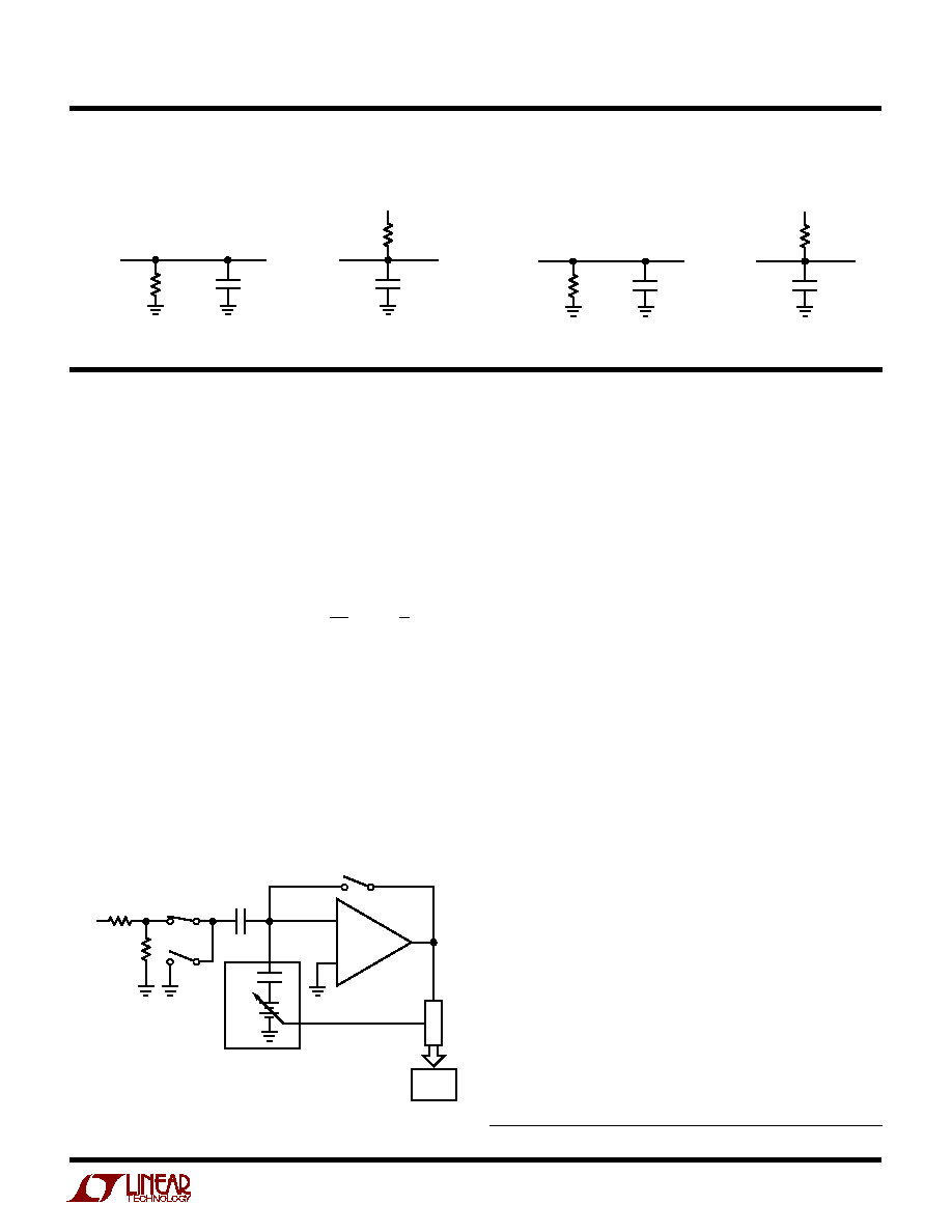
Figure 2. Analog Input Filtering
1605-1/2 F02
1000pF
33.2k
V
IN
CAP
A
IN
200
Internal Voltage Reference
The LTC1605-1/LTC1605-2 has an on-chip, temperature
compensated, curvature corrected, bandgap reference,
which is factory trimmed to 2.50V. The full-scale range of
the ADC is equal to (1.6V
REF
) or nominally 0V to 4V for the
LTC1605-1 and (
±
1.6V
REF
) or nominally
±
4V for the
LTC1605-2. The output of the reference is connected to
the input of a unity-gain buffer through a 4k resistor (see
Figure 3). The input to the buffer or the output of the
reference is available at REF (Pin 3). The internal refer-
ence can be overdriven with an external reference if more
accuracy is needed. The buffer output drives the internal
DAC and is available at CAP (Pin 4). The CAP pin can be
used to drive a steady DC load of less than 2mA. Driving
an AC load is not recommended because it can cause the
performance of the converter to degrade.
9
LTC1605-1/LTC1605-2
APPLICATIO
N
S I
N
FOR
M
ATIO
N
W
U
U
U
INPUT VOLTAGE (V)
≠ FS/2
0V
OUTPUT CODE
1605-1/2 F06b
011...111
011...110
000...001
000...000
111...111
111...110
100...000
100...001
≠1
LSB
1
LSB
BIPOLAR
ZERO
FS/2 ≠ 1LSB
FS = 8V
1LSB = FS/65536
Figure 6B. LTC1605-2 Bipolar Transfer Characteristics
CODE
0
500
1500
1000
2500
2000
4000
3500
3000
4500
COUNT
1605-1/2 F07
≠5 ≠4 ≠3 ≠2 ≠1
0
1
2
3
4
5
Figure 7. Histogram for 10000 Conversions
INPUT VOLTAGE (V)
0V
OUTPUT CODE
1605-1/2 F06a
111...111
111...110
000...000
000...001
1
LSB
UNIPOLAR
ZERO
FS ≠ 1LSB
FS = 4V
1LSB = FS/65536
Figure 6a. LTC1605-1 Unipolar Transfer Characteristics
Figure 5. 0V to 4V Input for the LTC1605-1 and
±
4V for the LTC1605-2 with Offset and Gain Trim
+
5
4
3
2
1
2.2
µ
F
+
2.2
µ
F
33.2k
1%
0V TO 4V
OR
±
4V
INPUT
200
1%
V
IN
AGND1
REF
CAP
AGND2
LTC1605-1
LTC1605-2
1605-1/2 F05
576k
R4
50k
R3
50k
OFFSET
TRIM
GAIN
TRIM
5V
S
S
≠
+
1605-1/2 F03
INTERNAL
CAPACITOR
DAC
BANDGAP
REFERENCE
V
ANA
4k
2.2
µ
F
CAP
(2.5V)
2.2
µ
F
REF
(2.5V)
4
3
Figure 3. Internal or External Reference Source
+
5
4
3
2
1
2.2
µ
F
+
2.2
µ
F
33.2k
1%
0V TO 4V
OR
±
4V
INPUT
200
1%
V
IN
AGND1
REF
CAP
AGND2
LTC1605-1
LTC1605-2
1605-1/2 F04
Figure 4. 0V to 4V Input for the LTC1605-1
and
±
4V for the LTC1605-2 Without Trim
10
LTC1605-1/LTC1605-2
APPLICATIO
N
S I
N
FOR
M
ATIO
N
W
U
U
U
DIGITAL INTERFACE
Internal Clock
The ADC has an internal clock that is trimmed to achieve
a typical conversion time of 7
µ
s. No external adjustments
are required and, with the typical acquisition time of 1
µ
s,
throughput performance of 100ksps is assured.
Timing and Control
Conversion start and data read are controlled by two
digital inputs: CS and R/C. To start a conversion and put
the sample-and-hold into the hold mode, bring CS and
R/C low for no less than 40ns. Once initiated, it cannot be
restarted until the conversion is complete. Converter
status is indicated by the BUSY output and this is low
while the conversion is in progress.
There are two modes of operation. The first mode is
shown in Figure 8. The digital input R/C is used to control
the start of conversion. CS is tied low. When R/C goes
low, the sample-and-hold goes into the hold mode and a
conversion is started. BUSY goes low and stays low
during the conversion and will go back high after the
conversion has been completed and the internal output
shift registers have been updated. R/C should remain low
for no less than 40ns. During the time R/C is low, the
Figure 8. Conversion Timing with Outputs Enabled After Conversion (CS Tied Low)
t
1
t
11
t
2
t
4
t
3
t
7
t
6
ACQUIRE
CONVERT
CONVERT
ACQUIRE
t
5
t
8
t
ACQ
t
CONV
t
9
PREVIOUS
DATA VALID
PREVIOUS
DATA VALID
HI-Z
NOT VALID
HI-Z
DATA
VALID
DATA
VALID
R/C
BUSY
MODE
DATA MODE
1605-1/2 F08
digital outputs are in a Hi-Z state. R/C should be brought
back high within 3
µ
s after the start of the conversion to
ensure that no errors occur in the digitized result. The
second mode, shown in Figure 9, uses the CS signal to
control the start of a conversion and the reading of the
digital output. In this mode, the R/C input signal should
be brought low no less than 10ns before the falling edge
of CS. The minimum pulse width for CS is 40ns. When CS
falls, BUSY goes low and will stay low until the end of the
conversion. BUSY will go high after the conversion has
been completed. The new data is valid when CS is
brought back low again to initiate a read. Again, it is
recommended that both R/C and CS return high within
3
µ
s after the start of the conversion.
Output Data
The output data can be read as a 16-bit word or it can be
read as two 8-bit bytes. The format of the output data is
straight binary for the LTC1605-1 and two's complement
for the LTC1605-2. The digital input pin BYTE is used to
control the two byte read. With the BYTE pin low, the first
eight MSBs are output on the D15 to D8 pins and the eight
LSBs are output on the D7 to D0 pins. When the BYTE pin
is taken high, the eight LSBs replace the eight MSBs
(Figure 10).
11
LTC1605-1/LTC1605-2
APPLICATIO
N
S I
N
FOR
M
ATIO
N
W
U
U
U
Figure 9. Using CS to Control Conversion and Read Timing
ACQUIRE
CONVERT
ACQUIRE
DATA
VALID
t
1
t
10
t
10
t
1
t
10
t
10
t
3
t
6
t
4
t
CONV
t
12
t
7
HI-Z
HI-Z
R/C
BUSY
CS
MODE
DATA BUS
1605-1/2 F09
Figure 10. Using CS and BYTE to Control Data Bus Read Timing
t
10
t
10
t
12
t
7
t
12
HI-Z
HI-Z
HI-Z
HI-Z
HIGH BYTE
LOW BYTE
LOW BYTE
HIGH BYTE
R/C
BYTE
CS
PINS 6 TO 13
PINS 15 TO 22
1605-1/2 F10
12
LTC1605-1/LTC1605-2
APPLICATIO
N
S I
N
FOR
M
ATIO
N
W
U
U
U
Dynamic Performance
FFT (Fast Fourier Transform) test techniques are used to
test the ADC's frequency response, distortion and noise
at the rated throughput. By applying a low distortion sine
wave and analyzing the digital output using an FFT
algorithm, the ADC's spectral content can be examined
for frequencies outside the fundamental. Figure 11 shows
a typical LTC1605-2 FFT plot which yields a SINAD of
87dB and THD of ≠101.1dB.
Signal-to-Noise Ratio
The Signal-to-Noise and Distortion Ratio (SINAD) is the
ratio between the RMS amplitude of the fundamental
input frequency to the RMS amplitude of all other fre-
quency components at the A/D output. The output is band
limited to frequencies from above DC and below half the
sampling frequency. Figure 11 shows a typical SINAD of
87dB with a 100kHz sampling rate and a 1kHz input.
where V
1
is the RMS amplitude of the fundamental
frequency and V
2
through V
N
are the amplitudes of the
second through Nth harmonics.
Board Layout, Power Supplies and Decoupling
Wire wrap boards are not recommended for high resolu-
tion or high speed A/D converters. To obtain the best
performance from the LTC1605-1/LTC1605-2, a printed
circuit board is required. Layout for the printed circuit
board should ensure the digital and analog signal lines
are separated as much as possible. In particular, care
should be taken not to run any digital track alongside an
analog signal track or underneath the ADC. The analog
input should be screened by AGND.
Figures 12 through 15 show a layout for a suggested
evaluation circuit which will help obtain the best perfor-
mance from the 16-bit ADC. Additional information re-
garding the evaluation circuit and Gerber files for the PC
board layout are available from Linear Technology or
your local sales office. Pay particular attention to the
design of the analog and digital ground planes. The
DGND pin of the LTC1605-1/LTC1605-2 can be tied to the
analog ground plane. Placing the bypass capacitor as
close as possible to the power supply, the reference and
reference buffer output is very important. Low imped-
ance common returns for these bypass capacitors are
essential to low noise operation of the ADC, and the PC
track width for these lines should be as wide as possible.
Also, since any potential difference in grounds between
the signal source and ADC appears as an error voltage in
series with the input signal, attention should be paid to
reducing the ground circuit impedance as much as
possible. The digital output latches and the onboard
sampling clock have been placed on the digital ground
plane. The two ground planes are tied together at the
power supply ground connection.
Figure 11. LTC1605-2 Nonaveraged 4096-Point FFT Plot
FREQUENCY (kHz)
0
MAGNITUDE (dB)
1605-1/2 G07/F11
5
10 15 20 25 30 35 40 45 50
0
≠10
≠20
≠30
≠40
≠50
≠60
≠70
≠80
≠90
≠100
≠110
≠120
≠130
f
SAMPLE
= 100kHz
f
IN
= 1kHz
SINAD = 87dB
THD = 101.1dB
SNR = 87.2dB
Total Harmonic Distortion
Total Harmonic Distortion (THD) is the ratio of the RMS
sum of all harmonics of the input signal to the fundamen-
tal itself. The out-of-band harmonics alias into the fre-
quency band between DC and half the sampling fre-
quency. THD is expressed as:
THD = 20log
V
2
2
+ V
3
2
+ V
4
2
... + V
N
2
V
1
13
LTC1605-1/LTC1605-2
APPLICATIO
N
S I
N
FOR
M
ATIO
N
W
U
U
U
Figure 12. Component Side Silkscreen for the Suggested LTC1605-1/LTC1605-2 Evaluation Circuit
ANALOG
GROUND PLANE
ANALOG
GROUND PLANE
DIGITAL
GROUND PLANE
Figure 13. Bottom Side Showing Analog Ground Plane
Figure 14. Component Side Showing Separate Analog
and Digital Ground Plane
14
LTC1605-1/LTC1605-2
D15
+
3
U6A
74HC221
A
B
Q
Q
CEXT
R21, 2k
RCEXT
15
1
2
4
13
CLK
1605-1/2 F15
D15
D14
U1
LTC1605-1
LTC1605-2
D13
D12
D11
C5
0.1
µ
F
R19
33.2k
1%
C3
0.1
µ
F
C16
1000pF
C4
2.2
µ
F
C2
2.2
µ
F
EXT
INT
V
REF
JP1
C17
10
µ
F
D10
D9
D8
D7
D6
D5
D4
D3
D2
D1
6
7
8
9
10
11
12
13
15
16
17
18
19
20
21
D0
D15
D15
D14
D13
D12
D11
D10
D9
D8
2
3
4
5
6
7
8
9
D14
D13
D12
D11
D10
D9
D8
D7
D6
D5
D4
D3
D2
D1
D0
4
R20
1K
3
U4B
74HC04
6
5
U4C
74HC04
C1
15PF
22
1
2
3
4
5
14
23
24
25
26
27
28
V
IN
Q0
U2
74HC574
19
D0
Q1
18
D1
Q2
17
D2
Q3
16
D3
Q4
15
D4
Q5
14
D5
Q6
13
D6
Q7
12
12
U4A
74HC04
D7
1
OC
11
CLK
2
7
6
5
4
3
U7
74HC160
CLR
LOAD
RCO
15
2
3
JP3
1
EXT
CLK
INT
2
3
JP5
1
V
CC
CS
GND
ENP
10
ENT
QD
11
D
QC
12
C
QB
13
B
QA
14
A
2
U8
1MHz, OSC
OUT
3
GND
1
NA
E2
GND
V
IN
7V TO 15V
E1
U5
LT1121
D16
MBR0520
C6
22
µ
F
10V
GND
13
2
V
IN
V
IN
4
U9
LT1019-2.5
TRIM
5
GND
1
NC1
2
INPUT
3
8
7
6
TEMP
NC2
HEATER
OUT
1
9
CLK
D0
D1
D2
D3
D4
D5
D6
D7
2
3
4
5
6
7
8
9
Q0
U3
74HC574
19
D0
Q1
18
D1
Q2
17
D2
Q3
16
D3
Q4
15
D4
Q5
14
D5
Q6
13
D6
Q7
12
D7
1
OC
11
CLK
AGND1
REF
CAP
AGND2
DGND
BYTE
R/C
CS
BUSY
V
ANA
V
DIG
C8
0.1
µ
F
C7
10
µ
F
V
KK
V
CC
V
KK
V
KK
V
DD
V
CC
R16
20
C9
0.1
µ
F
C10
0.1
µ
F
DIGITAL I.C. BYPASSING
C11
0.1
µ
F
C12
0.1
µ
F
V
CC
C13
0.1
µ
F
C14
0.1
µ
F
C15
10
µ
F
2
3
JP4
1
REVERSE
BYTE
NORNAL
V
CC
V
CC
V
CC
20
19
18
17
16
15
14
13
12
11
10
9
8
7
6
5
4
3
2
1
GND
GND
CLK
D15
D0
D1
D2
D3
D4
D5
D6
D7
D8
D9
D10
D11
D12
D13
D14
D15
R8, 1.2k
D8
R9, 1.2k
D9
R10, 1.2k
D10
R11, 1.2k
D11
R12, 1.2k
D12
R13, 1.2k
D13
R14, 1.2k
D14
R15, 1.2k
R0, 1.2k
D0
R1, 1.2k
D1
R2, 1.2k
D2
R3, 1.2k
D3
R4, 1.2k
D4
R5, 1.2k
D5
R6, 1.2k
D6
R7, 1.2k
D7
JP2
LED
ENABLE
10
11
U4E
74HC04
8
1
2
9
EXT_CLK
J1
1
2
A
IN
J2
R17
51
U4D
74HC04
R18
200
1%
APPLICATIO
N
S I
N
FOR
M
ATIO
N
W
U
U
U
Figure 15. LTC1605-1 Suggested Evaluation Circuit Schematic

15
LTC1605-1/LTC1605-2
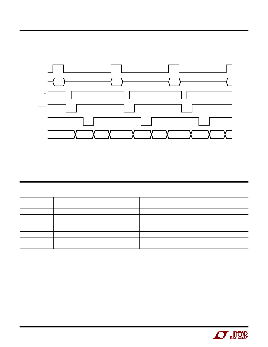
The circuit in Figure 16 is an example showing the LTC1605
16-bit A/D converter and LTC1391 8-channel MUX con-
nected to a 68HC11 controller. The LTC1605's 16-bit data
output is read in two 8-bit bytes using Pins 6 (MSB, Bit7)
through 13 (Bit8, Bit0), connected to the HC11's PORTC.
The MUX's 4-bit serial address data is sent using the
controller's SPI.
The process to convert a channel's input signal is shown
in sample listing A. It begins with shifting in the MUX's
channel data while the SS signal is a logic high. The MUX
channel address is latched on the falling edge of SS and the
chosen channel's input is applied at the LTC1605's input,
Pin 1. Through the processor's PORTA, a low-going pulse
is applied to the LTC1605's R/C pin, initiating a conver-
sion. The processor then monitors the BUSY output.
When this signal becomes a logic high, signaling the end
of conversion, the processor reads the high byte of the
conversion through PORTC. The low byte is read through
PORTC when the processor changes the BYTE signal to a
logic high. The timing relationship of the control signals
and data are shown in Figure 17.
Sample Listing A
*************************************************************************
*
*
* This example program selects the an LTC1391 MUX channel, initiates a *
* conversion, and retrieves conversion data. It stores the 16-bit data *
* in two consecutive memory locations. The program is designed for use *
* with the LTC1605's /CS tied to ground (see timing diagram in
*
* Figure 17).
*
*
*
*************************************************************************
*
*****************************************
* 68HC11 register definitions
*
*****************************************
*
PORTA
EQU
$1000
Parallel port A
*
Use Bit0 as an input for the LTC1605's /BUSY signal
*
Use Bit3 as an output driving the LTC1605's BYTE
*
input
PIOC
EQU
$1002
Parallel I/O control register
*
"STAF,STAI,CWOM,HNDS, OIN, PLS, EGA,INVB"
PORTC
EQU
$1003
Port C data register
*
"Bit7,Bit6,Bit5,Bit4,Bit3,Bit2,Bit1,Bit0"
DDRC
EQU
$1007
Port D data direction register
*
"Bit7,Bit6,Bit5,Bit4,Bit3,Bit2,Bit1,Bit0"
*
1 = output, 0 = input
PORTD
EQU
$1008
Port D data register
*
" - , - , SS* ,CSK ;MOSI,MISO,TxD ,RxD "
DDRD
EQU
$1009
Port D data direction register
SPCR
EQU
$1028
SPI control register
*
"SPIE,SPE ,DWOM,MSTR;SPOL,CPHA,SPR1,SPR0"
SPSR
EQU
$1029
SPI status register
*
"SPIF,WCOL, - ,MODF; - , - , - , - "
SPDR
EQU
$102A
SPI data register; Read-Buffer; Write-Shifter
*
* RAM variables to hold the LTC1605's 14 conversion result
*
DIN1
EQU
$00
This memory location holds the LTC1605's bits 15 - 08
DIN2
EQU
$01
This memory location holds the LTC1605's bits 07 - 00
MUX
EQU
$02
This memory location holds the MUX address data
*
TYPICAL APPLICATIO S
U

16
LTC1605-1/LTC1605-2
*****************************************
* Start GETDATA Routine
*
*****************************************
*
ORG
$C000
Program start location
INIT1
LDAA
#$03
0,0,0,0,0,0,1,1
*
"STAF=0,STAI=0,CWOM=0,HNDS=0, OIN=0, PLS=0, EGA=1,INVB=1"
STAA
PIOC
Ensures that the PIOC register's status is the same
*
as after a reset, necessary of simple Port D manipulation
LDAA
#$00
0,0,0,0,0,0,0,0
*
"Bits 7 - 0 are used as inputs for the LTC1605's data
STAA
DDRC
Direction of PortD's bit are now set as inputs
LDAA
#$2F
-,-,1,0;1,1,1,1
*
-, -, SS*-Hi, SCK-Lo, MOSI-Hi, MISO-Hi, X, X
STAA
PORTD
Keeps SS* a logic high when DDRD, Bit5 is set
LDAA
#$38
-,-,1,1;1,0,0,0
STAA
DDRD
SS* , SCK, MOSI are configured as Outputs
*
MISO, TxD, RxD are configured as Inputs
* DDRD's Bit5 is a 1 so that port D's SS* pin is a general output
LDAA
#$50
STAA
SPCR
The SPI is configured as Master, CPHA = 0, CPOL = 0
*
and the clock rate is E/2
*
(This assumes an E-Clock frequency of 4MHz. For higher
*
E-Clock frequencies, change the above value of $50 to a
*
value that ensures the SCK frequency is 2MHz or less.)
GETDATAPSHX
PSHY
PSHA
*
*****************************************
* Setup indecies
*
*****************************************
*
LDX
#$0
The X register is used as a pointer to the memory
*
locations that hold the conversion data
LDY
#$1000
*
*****************************************
* Ensure that a logic high is applied
*
* to the LTC1391's /CS and the
*
* LTC1605's R/C pins
*
*****************************************
*
BSET
PORTD,Y %00100000
This sets the SS* output bit to a logic
*
high, ensuring that the LTC1391's CS*
*
input is a logic high while clocking
*
MUX address data into the LTC1391
BSET
PORTA,Y %00010000
This sets the R/C* output bit to a logic
*
high, ensuring that the LTC1605's R/C*
*
input is a logic high before initiating
*
a conversion
*****************************************
TYPICAL APPLICATIO S
U

17
LTC1605-1/LTC1605-2
* Retrieve the MUX address from memory
*
* and send it to the LTC1391
*
*****************************************
*
LDAA
MUX
Retrieve the MUX address from memory
ORAA
#$08
Enable the selected MUX address
STAA
SPDR
Select the MUX channel
WAIT1
LDAA
SPSR
This loop waits for the SPI to complete a serial
*
transfer/exchange by reading the SPI Status Register
BPL
WAIT1
The SPIF (SPI transfer complete flag) bit is the SPSR's
*
MSB and is set to one at the end of an SPI transfer. The
*
branch will occur while SPIF is a zero.
BCLR
PORTD,Y %00100000
This forces a logic low on PORTD's SS*,
*
latching the MUXes data
*
*****************************************
* Initiate a LTC1605 conversion
*
*****************************************
*
BCLR
PORTA,Y %00010000
Initiate a conversion
BSET
PORTA,Y %00010000
This sets the LTC1605's R/C* to a logic
*
high
*
*****************************************
* Set the LTC1605's BYTE input low to
*
* ensure that the high byte is present
*
* during the first read
*
*****************************************
*
LDAA
PORTA
Get the contents of Port A
ANDA
#%11110111
Set Bit3 low
STAA
PORTA
Set the LTC1605's BYTE input low
*
*****************************************
* The next short loop ensures that the *
* LTC1605's conversion is finished *
* before starting the data transfer*
*****************************************
*
CONVENDLDAA
PORTA
Retrieve the contents of port A
ANDA
#%00000001
Look at Bit0
*
Bit0 = Lo; the LTC1605's conversion is not
*
complete
*
Bit0 = Hi; the LTC1605's conversion is complete
BEQ
CONVEND
Branch to the loop's beginning while Bit7
*
remains low
*
TYPICAL APPLICATIO S
U
18
LTC1605-1/LTC1605-2
*************************************************************************
* This routine retrieves the LTC1605's 16-bit data using two 8-bit
*
* reads. The BYTE input is manipulated through Port A's Bit3. During
*
* the first read when BYTE is low, the upper byte is read and stored in
*
* DIN1.During the second read when BYTE is high, the lower byte is
*
* read and stored in DIN2.
*
*************************************************************************
*
LDAA
PORTC
Retrieve the LTC1605's high byte
STAA
DIN1
Store the high byte
LDAA
PORTA
Get the contents of Port A
ORAA
#%00001000
Set Bit3 high
STAA
PORTA
Set the LTC1605's BYTE input high
LDAA
PORTC
Retrieve the LTC1605's low byte
STAA
DIN2
Store the high byte
PULA
Restore the A register
PULY
Restore the Y register
PULX
Restore the X register
RTS
V
DIG
V
ANA
LTC1605-1
LTC1605-2
D7/D15
D6/D14
D5/D13
D4/D12
D3/D11
D2/D10
D1/D9
D0/D8
28
27
6
7
8
9
10
11
12
13
18
V
+
D
LTC1391
V
≠
D
OUT
D
IN
CS
DLK
DGND
16
15
14
5V
0.1
µ
F
13
12
11
10
9
M0S1
SS
SPI
CLK
1
2
3
4
5
6
7
8
S0
S1
S2
S3
S4
S5
S6
S7
17
16
15
26
25
R/C
24
BYTE
23
PORTC, BIT7
PORTC, BIT6
PORTC, BIT5
PORTC, BIT4
PORTC, BIT3
PORTC, BIT2
PORTC, BIT1
PORTC, BIT0
PORTA, BIT0
PORTA, BIT4
PORTA, BIT3
20
19
14
1605-1/2 F16
1
4
5
3
22
21
V
IN
CAP
AGND2
DGND
REF
2
AGND1
BUSY
CS
2.2
µ
F
0.1
µ
F
0.1
µ
F
5V
5V
8
1
3
2
4
2.2
µ
F
33.2k
1%
200
1%
10
µ
F
1
µ
F
5V
+
+
≠
+
USE FOR LTC1605-2
1/2 LT1630
≠5V SUPPLY FOR
LTC1605-2
Figure 16. 8-Channel, 16-Bit Data Acquisition System with Interface to the 68HC11
TYPICAL APPLICATIO S
U
19
LTC1605-1/LTC1605-2
Information furnished by Linear Technology Corporation is believed to be accurate and reliable.
However, no responsibility is assumed for its use. Linear Technology Corporation makes no represen-
tation that the interconnection of its circuits as described herein will not infringe on existing patent rights.
G Package
28-Lead Plastic SSOP (0.209)
(LTC DWG # 05-08-1640)
Dimensions in inches (millimeters) unless otherwise noted.
PACKAGE DESCRIPTIO
N
U
G28 SSOP 1098
0.13 ≠ 0.22
(0.005 ≠ 0.009)
0
∞
≠ 8
∞
0.55 ≠ 0.95
(0.022 ≠ 0.037)
5.20 ≠ 5.38**
(0.205 ≠ 0.212)
7.65 ≠ 7.90
(0.301 ≠ 0.311)
1
2 3
4
5
6 7 8
9 10 11 12
14
13
10.07 ≠ 10.33*
(0.397 ≠ 0.407)
25
26
22 21 20 19 18 17 16 15
23
24
27
28
1.73 ≠ 1.99
(0.068 ≠ 0.078)
0.05 ≠ 0.21
(0.002 ≠ 0.008)
0.65
(0.0256)
BSC
0.25 ≠ 0.38
(0.010 ≠ 0.015)
NOTE: DIMENSIONS ARE IN MILLIMETERS
DIMENSIONS DO NOT INCLUDE MOLD FLASH. MOLD FLASH
SHALL NOT EXCEED 0.152mm (0.006") PER SIDE
DIMENSIONS DO NOT INCLUDE INTERLEAD FLASH. INTERLEAD
FLASH SHALL NOT EXCEED 0.254mm (0.010") PER SIDE
*
**
N28 1098
0.255
±
0.015*
(6.477
±
0.381)
1.370*
(34.789)
MAX
3
4
5
6
7
8
9
10
11
12
21
13
14
15
16
18
17
19
20
22
23
24
25
26
2
27
1
28
0.020
(0.508)
MIN
0.125
(3.175)
MIN
0.130
±
0.005
(3.302
±
0.127)
0.065
(1.651)
TYP
0.045 ≠ 0.065
(1.143 ≠ 1.651)
0.018
±
0.003
(0.457
±
0.076)
0.005
(0.127)
MIN
0.100
(2.54)
BSC
0.009 ≠ 0.015
(0.229 ≠ 0.381)
0.300 ≠ 0.325
(7.620 ≠ 8.255)
0.325
+0.035
≠0.015
+0.889
≠0.381
8.255
(
)
*THESE DIMENSIONS DO NOT INCLUDE MOLD FLASH OR PROTRUSIONS.
MOLD FLASH OR PROTRUSIONS SHALL NOT EXCEED 0.010 INCH (0.254mm)
N Package
28-Lead PDIP (Narrow 0.300)
(LTC DWG # 05-08-1510)
20
LTC1605-1/LTC1605-2
©
LINEAR TECHNOLOGY CORPORATION 1999
160512f LT/TP 0999 4K ∑ PRINTED IN THE USA
Linear Technology Corporation
1630 McCarthy Blvd., Milpitas, CA 95035-7417
(408) 432-1900
q
FAX: (408) 434-0507
q
www.linear-tech.com
PART NUMBER
DESCRIPTION
COMMENTS
LT
Æ
1019-2.5
Precision Bandgap Reference
0.05% Max, 5ppm/
∞
C Max
LTC1274/LTC1277
Low Power 12-Bit, 100ksps ADCs
10mW Power Dissipation, Parallel/Byte Interface
LTC1415
Single 5V, 12-Bit, 1.25Msps ADC
55mW Power Dissipation, 72dB SINAD
LTC1419
Low Power 14-Bit, 800ksps ADC
True 14-Bit Linearity, 81.5dB SINAD, 150mW Dissipation
LT1460-2.5
Micropower Precision Series Reference
0.075% Max, 10ppm/
∞
C Max, Only 130
µ
A Supply Current
LTC1594/LTC1598
Micropower 4-/8-Channel 12-Bit ADCs
Serial I/O, 3V and 5V Versions
LTC1604
16-Bit, 333ksps Sampling ADC
±
2.5V Input, 90dB SINAD, 100dB THD
LTC1605
Low Power 100ksps 16-Bit ADC
Single 5V,
±
10V Inputs
RELATED PARTS
TYPICAL APPLICATIO
U
R/C
BUSY
BYTE
ADC
DATA
MUX
CS
MUX
DATA
HI BYTE
LO BYTE
DATA 0
DATA 1
HI BYTE
LO BYTE
HI BYTE
LO BYTE
CH0
CH1
CH2
1605-1/2 F17
Figure 17. This Is the Timing Relationship Between the Selected MUX Channel, Its Conversion Data
and the ADC and MUX Control Signals When Using the Sample Program In Listing 1. The Conversion
Process Is Latency Free: the Data Is Always Generated Based On the Currently Selected MUX Input