 | –≠–ª–µ–∫—Ç—Ä–æ–Ω–Ω—ã–π –∫–æ–º–ø–æ–Ω–µ–Ω—Ç: LTC1606 | –°–∫–∞—á–∞—Ç—å:  PDF PDF  ZIP ZIP |
1
LTC1606
16-Bit, 250ksps,
Single Supply ADC
March 2000
DESCRIPTIO
N
U
FEATURES
The LTC
Æ
1606 is a 250ksps, sampling 16-bit A/D con-
verter that draws only 75mW (typical) from a single 5V
supply. This easy-to-use device includes sample-and-
hold, precision reference, switched capacitor successive
approximation A/D and trimmed internal clock.
The LTC1606's input range is an industry standard
±
10V.
Maximum DC specs include
±
2.0LSB INL and 16 bits no
missing codes over temperature. An external reference
can be used if greater accuracy over temperature is
needed.
The 90dB signal-to-noise ratio offers an improvement of
3dB over competing devices, and the RMS transition noise
is reduced (0.65LSB vs 1LSB) relative to competitive
parts.
The ADC has a microprocessor compatible, 16-bit or two
byte parallel output port. A convert start input and a data
ready signal (BUSY) ease connections to FIFOs, DSPs and
microprocessors.
s
Sample Rate: 250ksps
s
Single 5V Supply
s
Bipolar Input Range:
±
10V
s
Signal-to-Noise Ratio: 90dB Typ
s
Power Dissipation: 75mW Typ
s
Integral Nonlinearity:
±
2.0LSB Max
s
Guaranteed No Missing Codes
s
Operates with Internal or External Reference
s
Internal Synchronized Clock
s
28-Pin SSOP Package
s
Improved 2nd Source to AD976A and ADS7805
s
Industrial Process Control
s
Multiplexed Data Acquisition Systems
s
High Speed Data Acquisition for PCs
s
Digital Signal Processing
APPLICATIO
N
S
U
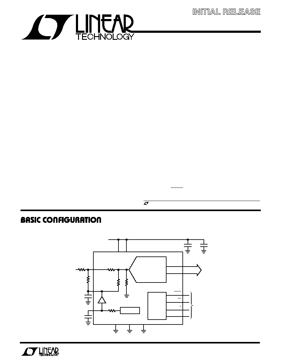
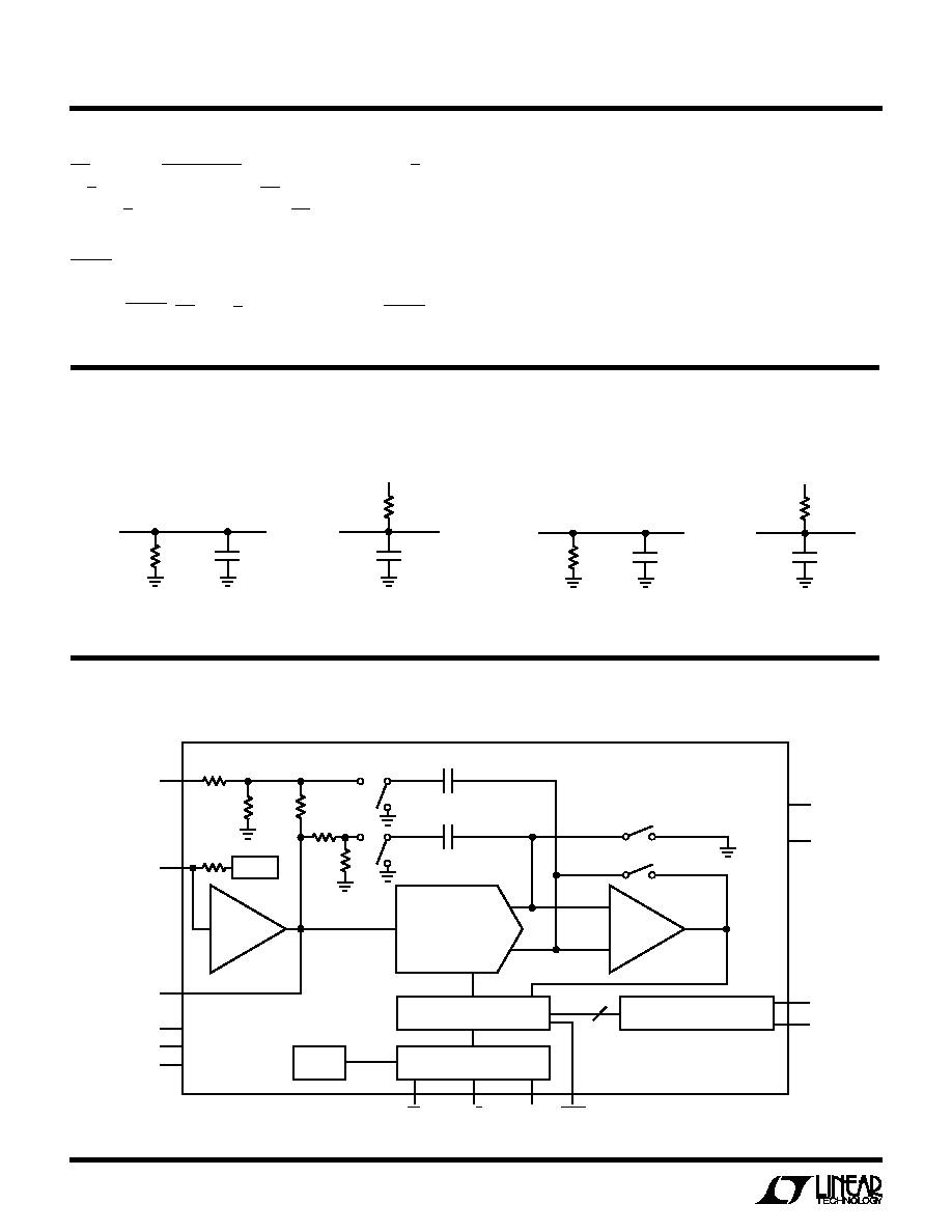
Low Power, 250kHz, 16-Bit Sampling ADC on 5V Supply
, LTC and LT are registered trademarks of Linear Technology Corporation.
4k
7.35k
200
REFERENCE
2.5k
9k
16-BIT
SAMPLING ADC
D15 TO D0
33.2k
10
µ
F
10
µ
F
0.1
µ
F
2.2
µ
F
±
10V
INPUT
V
IN
CAP
REF
AGND1
1
4
3
2
AGND2
5
DGND
14
CONTROL
LOGIC AND
TIMING
BUSY
BYTE
CS
R/C
28
27
6 TO 13
15 TO 22
26
25
24
23
DIGITAL
CONTROL
SIGNALS
1606 TA01
16-BIT
OR 2 BYTE
PARALLEL
BUS
5V
V
DIG
V
ANA
1.64x
BUFFER
4.096V
2.5V
Information furnished by Linear Technology Corporation is believed to be accurate and reliable.
However, no responsibility is assumed for its use. Linear Technology Corporation makes no represen-
tation that the interconnection of its circuits as described herein will not infringe on existing patent rights.
Final Electrical Specifications
2
LTC1606
LTC1606
LTC1606A
PARAMETER
CONDITIONS
MIN
TYP
MAX
MIN
TYP
MAX
UNITS
Resolution
q
16
16
Bits
No Missing Codes
q
15
16
Bits
Transition Noise
0.65
0.65
LSB
RMS
Integral Linearity Error
(Note 7)
q
±
3
±
2
LSB
Bipolar Zero Error
Ext. Reference = 2.5V (Note 8)
q
±
10
±
10
mV
Bipolar Zero Error Drift
±
2
±
2
ppm/
∞
C
Full-Scale Error Drift
±
7
±
5
ppm/
∞
C
Full-Scale Error
Ext. Reference = 2.5V (Notes 12, 13)
q
±
0.50
±
0.25
%
Full-Scale Error Drift
Ext. Reference = 2.5V
±
2
±
2
ppm/
∞
C
Power Supply Sensitivity
V
ANA
= V
DIG
= V
DD
V
DD
= 5V
±
5% (Note 9)
±
8
±
8
LSB
A
U
G
W
A
W
U
W
A
R
BSOLUTE
XI
TI
S
W
U
U
PACKAGE/ORDER I FOR ATIO
ORDER PART
NUMBER
(Notes 1, 2)
V
ANA
.......................................................................... 7V
V
DIG
to V
ANA
........................................................... 0.3V
V
DIG
........................................................................... 7V
Ground Voltage Difference
DGND, AGND1 and AGND2 ..............................
±
0.3V
Analog Inputs (Note 3)
V
IN
.....................................................................
±
25V
CAP ............................ V
ANA
+ 0.3V to AGND2 ≠ 0.3V
REF .................................... Indefinite Short to AGND2
Momentary Short to V
ANA
Digital Input Voltage (Note 4) ........ V
DGND
≠ 0.3V to 10V
Digital Output Voltage ........ V
DGND
≠ 0.3V to V
DIG
+ 0.3V
Power Dissipation .............................................. 500mW
Operating Ambient Temperature Range
LTC1606AC/LTC1606C ............................ 0
∞
C to 70
∞
C
LTC1606AI/LTC1606I ......................... ≠ 40
∞
C to 85
∞
C
Storage Temperature Range ................. ≠ 65
∞
C to 150
∞
C
Lead Temperature (Soldering, 10 sec).................. 300
∞
C
LTC1606ACG
LTC1606AIG
LTC1606CG
LTC1606IG
T
JMAX
= 125
∞
C,
JA
= 95
∞
C/W
Consult factory for Military grade parts.
CO
N
VERTER CHARACTERISTICS
U
1
2
3
4
5
6
7
8
9
10
11
12
13
14
28
27
26
25
24
23
22
21
20
19
18
17
16
15
V
IN
AGND1
REF
CAP
AGND2
D15 (MSB)
D14
D13
D12
D11
D10
D9
D8
DGND
V
DIG
V
ANA
BUSY
CS
R/C
BYTE
D0
D1
D2
D3
D4
D5
D6
D7
G PACKAGE
28-LEAD PLASTIC SSOP
TOP VIEW
The
q
indicates specifications which apply over the full operating
temperature range, otherwise specifications are at T
A
= 25
∞
C. (Notes 5, 6)
3
LTC1606
LTC1606
LTC1606A
SYMBOL
PARAMETER
CONDITIONS
MIN
TYP
MAX
MIN
TYP
MAX
UNITS
S/(N + D)
Signal-to-(Noise + Distortion) Ratio 1kHz Input Signal (Note 14)
90
90
dB
10kHz Input Signal
90
87
90
dB
20kHz, ≠ 60dB Input Signal
30
30
dB
THD
Total Harmonic Distortion
1kHz Input Signal, First 5 Harmonics
≠102
≠ 102
dB
10kHz Input Signal, First 5 Harmonics
≠94
≠89
≠ 94
dB
Peak Harmonic or Spurious Noise
1kHz Input Signal
≠102
≠ 102
dB
10kHz Input Signal
≠94
≠ 94
dB
Full-Power Bandwidth
(Note 15)
275
275
kHz
Aperture Delay
40
40
ns
Aperture Jitter
Sufficient to Meet AC Specs Sufficient to Meet AC Specs
Transient Response
Full-Scale Step (Note 9)
2
2
µ
s
Overvoltage Recovery
(Note 16)
150
150
ns
DY
N
A
M
IC ACCURACY
U
W
I
N
TER
N
AL REFERE
N
CE CHARACTERISTICS
U
U
U
LTC1606/LTC1606A
PARAMETER
CONDITIONS
MIN
TYP
MAX
UNITS
V
REF
Output Voltage
I
OUT
= 0
q
2.470
2.500
2.520
V
V
REF
Output Tempco
I
OUT
= 0
±
5
ppm/
∞
C
Internal Reference Source Current
1
µ
A
External Reference Voltage for Specified Linearity
(Notes 9, 10)
2.30
2.50
2.70
V
External Reference Current Drain
Ext. Reference = 2.5V (Note 9)
q
100
µ
A
CAP Output Voltage
I
OUT
= 0
4.096
V
(Notes 5, 14)
The
q
indicates specifications which apply over the full
operating temperature range, otherwise specifications are at T
A
= 25
∞
C. (Note 5)
The
q
indicates specifications which apply over the full operating temperature range, otherwise
specifications are at T
A
= 25
∞
C. (Note 5)
LTC1606/LTC1606A
SYMBOL
PARAMETER
CONDITIONS
MIN
TYP
MAX
UNITS
V
IN
Analog Input Range (Note 9)
4.75V
V
ANA
5.25V, 4.75V
V
DIG
5.25V
q
±
10
V
C
IN
Analog Input Capacitance
10
pF
R
IN
Analog Input Impedance
10
k
A
N
ALOG I
N
PUT
U
U
4
LTC1606
LTC1606/LTC1606A
SYMBOL
PARAMETER
CONDITIONS
MIN
TYP
MAX
UNITS
f
SAMPLE(MAX)
Maximum Sampling Frequency
q
250
kHz
t
CONV
Conversion Time
q
2.5
µ
s
t
ACQ
Acquisition Time
q
1.5
µ
s
t
1
Convert Pulse Width
(Note 11)
q
40
ns
t
2
Data Valid Delay After R/C
(Note 9)
q
2.5
µ
s
t
3
BUSY Delay from R/C
C
L
= 30pF
q
65
ns
t
4
BUSY Low
q
2.5
µ
s
t
5
BUSY Delay After End of Conversion
100
ns
t
6
Aperture Delay
40
ns
t
7
Bus Relinquish Time
q
15
50
ns
t
8
BUSY Delay After Data Valid
q
20
90
ns
t
9
Previous Data Valid After R/C
2
µ
s
t
10
R/C to CS Setup Time
(Notes 9, 10)
q
5
ns
t
11
Time Between Conversions
q
4
µ
s
t
12
Bus Access
C
L
= 30pF, (Notes 10)
q
15
60
ns
Byte Delay
C
L
= 30pF, (Notes 9, 10)
q
15
60
ns
LTC1606/LTC1606A
SYMBOL
PARAMETER
CONDITIONS
MIN
TYP
MAX
UNITS
V
IH
High Level Input Voltage
V
DD
= 5.25V
q
2.4
V
V
IL
Low Level Input Voltage
V
DD
= 4.75V
q
0.8
V
I
IN
Digital Input Current
V
IN
= 0V to V
DD
q
±
10
µ
A
C
IN
Digital Input Capacitance
5
pF
V
OH
High Level Output Voltage
V
DD
= 4.75V
I
O
= ≠10
µ
A
4.5
V
I
O
= ≠ 200
µ
A
q
4.0
V
V
OL
Low Level Output Voltage
V
DD
= 4.75V
I
O
= 160
µ
A
0.05
V
I
O
= 1.6mA
q
0.10
0.4
V
I
OZ
Hi-Z Output Leakage D15 to D0
V
OUT
= 0V to V
DD
, CS High
q
±
10
µ
A
C
OZ
Hi-Z Output Capacitance D15 to D0
CS High (Note 9)
q
15
pF
I
SOURCE
Output Source Current
V
OUT
= 0V
≠10
mA
I
SINK
Output Sink Current
V
OUT
= V
DD
10
mA
TI
M
I
N
G CHARACTERISTICS
W
U
DIGITAL I
N
PUTS A
N
D DIGITAL OUTPUTS
U
U
The
q
indicates specifications which apply over the full
operating temperature range, otherwise specifications are at T
A
= 25
∞
C. (Note 5)
The
q
indicates specifications which apply over the full operating temperature
range, otherwise specifications are at T
A
= 25
∞
C. (Note 5)

5
LTC1606
Note 1: Absolute Maximum Ratings are those values beyond which the life
of a device may be impaired.
Note 2: All voltage values are with respect to ground with DGND, AGND1
and AGND2 wired together (unless otherwise noted).
Note 3: When these pin voltages are taken below ground or above V
ANA
=
V
DIG
= V
DD
, they will be clamped by internal diodes. This product can
handle input currents of greater than 100mA below ground or above V
DD
without latch-up.
Note 4: When these pin voltages are taken below ground, they will be
clamped by internal diodes. This product can handle input currents of
90mA below ground without latchup. These pins are not clamped to V
DD
.
Note 5: V
DD
= 5V, f
SAMPLE
= 250kHz, t
r
= t
f
= 5ns unless otherwise
specified.
Note 6: Linearity, offset and full-scale specifications apply for a V
IN
input
with respect to ground.
Note 7: Integral nonlinearity is defined as the deviation of a code from a
straight line passing through the actual end points of the transfer curve.
The deviation is measured from the center of the quantization band.
Note 8: Bipolar offset is the offset voltage measured from ≠ 0.5 LSB when
the output code flickers between 0000 0000 0000 0000 and 1111 1111
1111 1111.
Note 9: Guaranteed by design, not subject to test.
Note 10: Recommended operating conditions.
Note 11: With CS low the falling R/C edge starts a conversion. If R/C
returns high at a critical point during the conversion, it can create errors.
For best results, ensure that R/C returns high within 1
µ
s after the start of
the conversion.
Note 12: As measured with fixed resistors shown in Figure 4. Adjustable to
zero with external potentiometer.
Note 13: Full-scale error is the worst-case of ≠FS or +FS untrimmed
deviation from ideal first and last code transitions, divided by the transition
voltage (not divided by the full-scale range) and includes the effect of
offset error.
Note 14: All specifications in dB are referred to a full-scale
±
10V input.
Note 15: Full-power bandwidth is defined as full-scale input frequency at
which a signal-to-(noise + distortion) degrades to 60dB or 10 bits of
accuracy.
Note 16: Recovers to specified performance after (2
∑ FS) input
overvoltage.
POWER REQUIRE
M
E
N
TS
W
U
LTC1606/LTC1606A
SYMBOL
PARAMETER
CONDITIONS
MIN
TYP
MAX
UNITS
V
DD
Positive Supply Voltage
(Notes 9, 10)
4.75
5.25
V
I
DD
Positive Supply Current
q
15
20
mA
P
DIS
Power Dissipation
q
75
100
mW
The
q
indicates specifications which apply over the full operating temperature
range, otherwise specifications are at T
A
= 25
∞
C. (Note 5)
V
IN
(Pin 1): Analog Input. Connect through a 200
resistor to the analog input. Full-scale input range is
±
10V.
AGND1 (Pin 2): Analog Ground. Tie to analog ground
plane.
REF (Pin 3): 2.5V Reference Output. Bypass with 2.2
µ
F
tantalum capacitor. Can be driven with an external refer-
ence.
CAP (Pin 4): Reference Buffer Output. Bypass with 10
µ
F
tantalum capacitor. The capacitor output voltage is 4.096V
when REF = 2.5V.
AGND2 (Pin 5): Analog Ground. Tie to analog ground
plane.
D15 to D8 (Pins 6 to 13): Three-State Data Outputs.
Hi-Z state when CS is high or when R/C is low.
DGND (Pin 14): Digital Ground.
D7 to D0 (Pins 15 to 22): Three-State Data Outputs.
Hi-Z state when CS is high or when R/C is low.
BYTE (Pin 23): Byte Select. With BYTE low, data will be
output with Pin 6 (D15) being the MSB and Pin 22 (D0)
being the LSB. With BYTE high the upper eight bits and
the lower eight bits will be switched. The MSB is output
on Pin 15 and bit 8 is output on Pin 22. Bit 7 is output on
Pin 6 and the LSB is output on Pin 13.
R/C (Pin 24): Read/Convert Input. With CS low, a falling
edge on R/C puts the internal sample-and-hold into the
hold state and starts a conversion. With CS low, a rising
edge on R/C enables the output data bits.
PI
N
FU
N
CTIO
N
S
U
U
U
6
LTC1606
PI
N
FU
N
CTIO
N
S
U
U
U
CS (Pin 25): Chip Select. Internally OR'd with R/C. With
R/C low, a falling edge on CS will initiate a conversion.
With R/C high, a falling edge on CS will enable the output
data.
BUSY (Pin 26): Output Shows Converter Status. It is low
when a conversion is in progress. Data valid on the rising
edge of BUSY. CS or R/C must be high when BUSY rises
TEST CIRCUITS
Load Circuit for Access Timing
1k
30pF
30pF
DBN
DBN
1k
5V
1606 TC01
A. Hi-Z TO V
OH
AND V
OL
TO V
OH
B. Hi-Z TO V
OL
AND V
OH
TO V
OL
Load Circuit for Output Float Delay
1k
30pF
30pF
DBN
DBN
1k
5V
1606 TC02
A. V
OH
TO Hi-Z
B. V
OL
TO Hi-Z
FU
N
CTIO
N
AL BLOCK DIAGRA
U
U
W
16-BIT CAPACITIVE DAC
COMP
REF BUF
1.64x
2.5V REF
CAP
(4.096V)
C
SAMPLE
C
SAMPLE
∑
∑
∑
D15
D0
BUSY
CONTROL LOGIC
R/C
BYTE
INTERNAL
CLOCK
CS
ZEROING SWITCHES
V
DIG
V
ANA
V
IN
REF
AGND1
AGND2
DGND
16
1606 BD
+
≠
SUCCESSIVE APPROXIMATION
REGISTER
OUTPUT LATCHES
4k
7.35k
2.5k
9k
or another conversion will start without time for signal
acquisition.
V
ANA
(Pin 27): 5V Analog Supply. Bypass to ground with
a 0.1
µ
F ceramic and a 10
µ
F tantalum capacitor.
V
DIG
(Pin 28): 5V Digital Supply. Connect directly to Pin
27.
7
LTC1606
Conversion Details
The LTC1606 uses a successive approximation algorithm
and an internal sample-and-hold circuit to convert an
analog signal to a 16-bit or two byte parallel output. The
ADC is complete with a precision reference and an internal
clock. The control logic provides easy interface to micro-
processors and DSPs. (Please refer to the Digital Interface
section for the data format.)
Conversion start is controlled by the CS and R/C inputs. At
the start of conversion the successive approximation
register (SAR) is reset. Once a conversion cycle has
begun, it cannot be restarted.
During the conversion, the internal 16-bit capacitive DAC
output is sequenced by the SAR from the most significant
bit (MSB) to the least significant bit (LSB). Referring to
Figure 1, V
IN
is connected through the resistor divider to
the sample-and-hold capacitor during the acquire phase
and the comparator offset is nulled by the autozero switches.
In this acquire phase, a minimum delay of 1.5
µ
s will
provide enough time for the sample-and-hold capacitor to
acquire the analog signal. During the convert phase, the
autozero switches open, putting the comparator into the
compare mode. The input switch switches C
SAMPLE
to
ground, injecting the analog input charge onto the sum-
ming junction. This input charge is successively com-
pared with the binary-weighted charges supplied by the
capacitive DAC. Bit decisions are made by the high speed
comparator. At the end of a conversion, the DAC output
balances the V
IN
input charge. The SAR contents (a 16-bit
data word) that represents the V
IN
are loaded into the
16-bit output latches.
Driving the Analog Inputs
The nominal input range for the LTC1606 is
±
10V or
(
±
4 ∑ V
REF
) and the input is overvoltage protected to
±
25V.
The input impedance is typically 10k
, therefore, it should
be driven with a low impedance source. Wideband noise
coupling into the input can be minimized by placing a
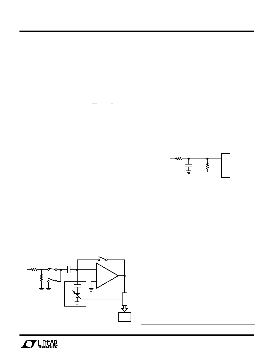
1000pF capacitor at the input as shown in Figure 2. An
NPO-type capacitor gives the lowest distortion. Place the
capacitor as close to the device input pin as possible. If an
amplifier is to be used to drive the input, care should be
taken to select an amplifier with adequate accuracy, linear-
ity and noise for the application. The following list is a
summary of the op amps that are suitable for driving the
LTC1606. More detailed information is available in the
Linear Technology data books and LinearView
TM
CD-ROM.
LT1007 - Low noise precision amplifier. 2.7mA supply
current
±
5V to
±
15V supplies. Gain bandwidth product
8MHz. DC applications.
LT1097 - Low cost, low power precision amplifier. 300
µ
A
supply current.
±
5V to
±
15V supplies. Gain bandwidth
product 0.7MHz. DC applications.
LT1227 - 140MHz video current feedback amplifier. 10mA
supply current.
±
5V to
±
15V supplies. Low noise and low
distortion.
LT1360 - 37MHz voltage feedback amplifier. 3.8mA sup-
ply current.
±
5V to
±
15V supplies. Good AC/DC specs.
LT1363 - 50MHz voltage feedback amplifier. 6.3mA sup-
ply current. Good AC/DC specs.
LT1364/LT1365 - Dual and quad 50MHz voltage feedback
amplifiers. 6.3mA supply current per amplifier. Good AC/
DC specs.
LT1468 - 90MHz 22V/
µ
s 16-bit accurate amplifier.
V
DAC
1606 ∑ F01
+
≠
C
DAC
DAC
SAMPLE
HOLD
C
SAMPLE
S
A
R
16-BIT
LATCH
COMPARATOR
SAMPLE
SI
R
IN2
R
IN1
V
IN
APPLICATIO
N
S I
N
FOR
M
ATIO
N
W
U
U
U
Figure 1. LTC1606 Simplified Equivalent Circuit
1606 ∑ F02
1000pF
33.2k
V
IN
CAP
A
IN
200
Figure 2. Analog Input Filtering
LinearView is a trademark of Linear Technology Corporation
8
LTC1606
Internal Voltage Reference
The LTC1606 has an on-chip, temperature compensated,
curvature corrected, bandgap reference, which is factory
trimmed to 2.50V. The full-scale range of the ADC is equal
to (
±
4 ∑ V
REF
) or nominally
±
10V. The output of the
reference is connected to the input of a buffer (1.64x)
through a 4k resistor (see Figure 3). The input to the buffer
or the output of the reference is available at REF (Pin 3).
The internal reference can be overdriven with an external
reference if more accuracy is needed. The buffer output
drives the internal DAC and is available at CAP (Pin 4). The
CAP pin can be used to drive a steady DC load of less than
2mA. Driving an AC load is not recommended because it
can cause the performance of the converter to degrade.
For minimum code transition noise, the REF pin and the
CAP pin should each be decoupled with a capacitor to
filter wideband noise from the reference and the buffer
(2.2
µ
F tantalum for the REF pin and 10
µ
F tantalum for the
CAP pin).
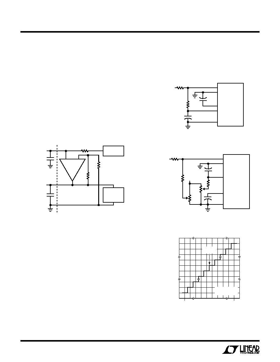
Offset and Gain Adjustments
The LTC1606 offset and full-scale errors have been trimmed
at the factory with the external resistors shown in Figure
4. This allows for external adjustment of offset and full
scale in applications where absolute accuracy is impor-
tant. See Figure 5 for the offset and gain trim circuit. First,
adjust the offset to zero by adjusting resistor R3. Apply an
input voltage of ≠152.6
µ
V (≠ 0.5LSB) and adjust R3 so the
code is changing between 1111 1111 1111 1111 and 0000
0000 0000 0000. The gain error is trimmed by adjusting
resistor R4. An input voltage of 9.999542V (+FS ≠ 1.5LSB)
is applied to V
IN
and R4 is adjusted until the output code
is changing between 0111 1111 1111 1110 and 0111
1111 1111 1111. Figure 6 shows the bipolar transfer
characteristic of the LTC1606.
Figure 3. Internal or External Reference Source
APPLICATIO
N
S I
N
FOR
M
ATIO
N
W
U
U
U
+
5
4
3
2
1
10
µ
F
+
2.2
µ
F
33.2k
1%
±
10V INPUT
200
1%
V
IN
AGND1
REF
CAP
AGND2
LTC1606
1606 ∑ F04
Figure 4.
±
10V Input Without Trim
+
5
4
3
2
1
10
µ
F
+
2.2
µ
F
33.2k
1%
±
10V INPUT
200
1%
V
IN
AGND1
REF
CAP
AGND2
LTC1606
1606 ∑ F05
576k
R4
50k
R3
50k
5V
Figure 5.
±
10V Input with Offset and Gain Trim
INPUT VOLTAGE (V)
0V
OUTPUT CODE
≠1
LSB
1606 ∑ F06
011...111
011...110
000...001
000...000
100...000
100...001
111...110
1
LSB
BIPOLAR
ZERO
111...111
FS/2 ≠ 1LSB
≠FS/2
FS = 20V
1LSB = FS/65536
Figure 6. LTC1606 Bipolar Transfer Characteristics
≠
+
1606 ∑ F03
INTERNAL
CAPACITOR
DAC
BANDGAP
REFERENCE
4k
10
µ
F
CAP
(4.096V)
2.2
µ
F
REF
(2.5V)
4
3
R
0.64R

9
LTC1606
DC Performance
One way of measuring the transition noise associated with
a high resolution ADC is to use a technique where a DC
signal is applied to the input of the ADC and the resulting
output codes are collected over a large number of conver-
sions. For example in Figure 7, the distribution of output
code is shown for a DC input that has been digitized 4096
times. The distribution is Gaussian and the RMS code
transition is about 0.65LSB.
DIGITAL INTERFACE
Internal Clock
The ADC has an internal clock that is trimmed to achieve
a typical conversion time of 2.3
µ
s. No external adjust-
ments are required and, with the typical acquisition time of
1
µ
s, throughput performance of 250ksps is assured.
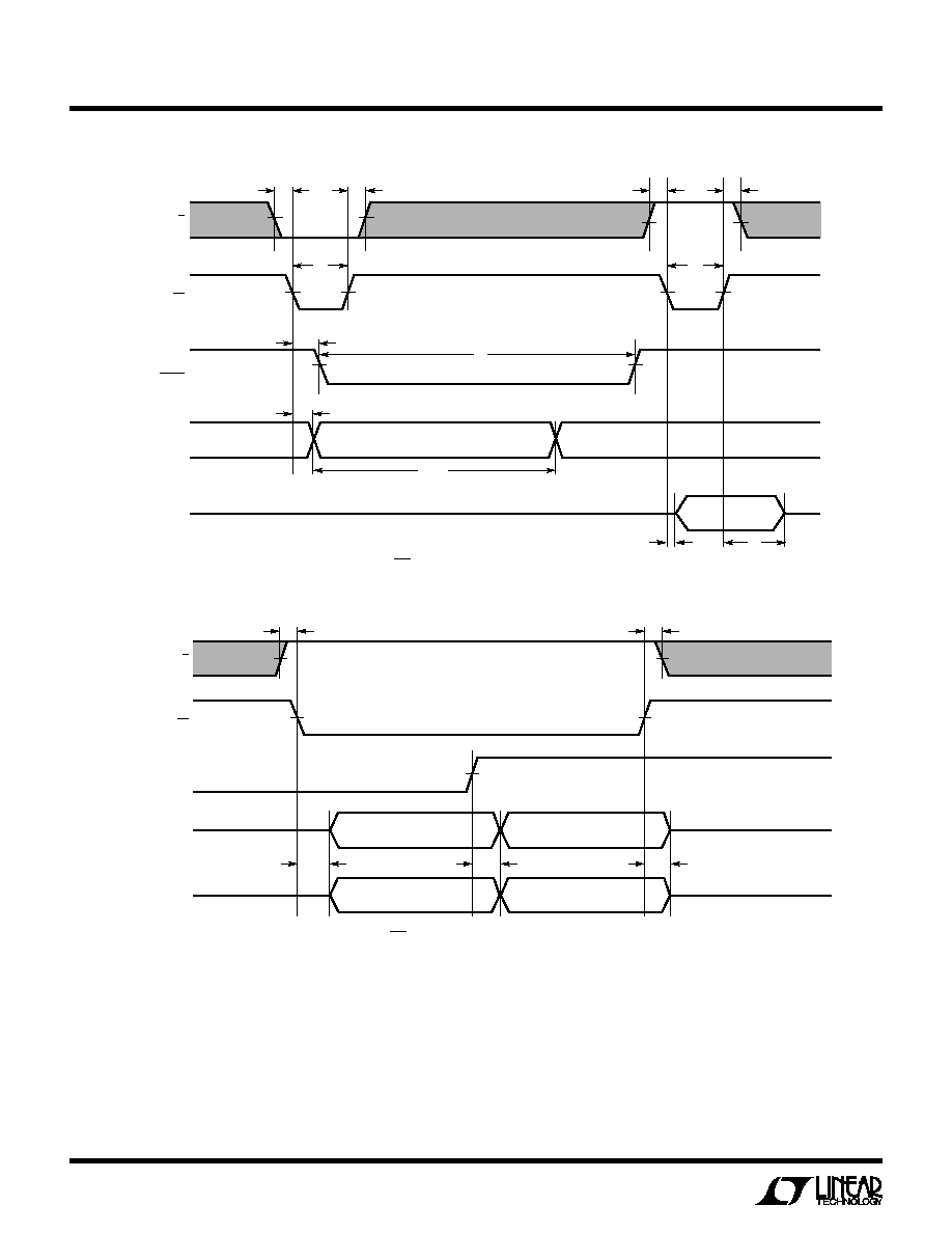
Timing and Control
Conversion start and data read are controlled by two
digital inputs: CS and R/C. To start a conversion and put
the sample-and-hold into the hold mode, bring CS and
R/C low for no less than 40ns. Once initiated, it cannot be
restarted until the conversion is complete. Converter
status is indicated by the BUSY output and this is low while
the conversion is in progress.
There are two modes of operation. The first mode is shown
in Figure 8. The digital input R/C is used to control the start
of conversion. CS is tied low. When R/C goes low, the
sample-and-hold goes into the hold mode and a conver-
sion is started. BUSY goes low and stays low during the
conversion and will go back high after the conversion has
been completed and the internal output shift registers
have been updated. R/C should remain low for no less than
40ns. During the time R/C is low, the digital outputs are in
a Hi-Z state. R/C should be brought back high within 1
µ
s
after the start of the conversion to ensure that no errors
occur in the digitized result. The second mode, shown in
Figure 9, uses the CS signal to control the start of a
conversion and the reading of the digital output. In this
mode the R/C input signal should be brought low no less
than 10ns before the falling edge of CS. The minimum
pulse width for CS is 40ns. When CS falls, BUSY goes low
and will stay low until the end of the conversion. BUSY will
go high after the conversion has been completed. The new
data is valid when CS is brought back low again to initiate
a read. Again, it is recommended that both R/C and CS
return high within 1
µ
s after the start of the conversion.
APPLICATIO
N
S I
N
FOR
M
ATIO
N
W
U
U
U
t
1
t
11
t
2
t
4
t
3
t
7
t
6
ACQUIRE
CONVERT
CONVERT
ACQUIRE
t
5
t
8
t
ACQ
t
CONV
t
9
PREVIOUS
DATA VALID
PREVIOUS
DATA VALID
Hi-Z
NOT VALID
Hi-Z
DATA
VALID
DATA
VALID
R/C
BUSY
MODE
DATA MODE
1606 ∑ F08
Figure 7. Histogram for 4096 Conversions
Figure 8. Conversion Timing with Outputs Enabled After Conversion (CS Tied Low)
2500
2000
1500
1000
500
0
≠3
≠2
≠1
0
1
2
3
4
COUNTS
CODE
1606 ∑ F07
10
LTC1606
APPLICATIO
N
S I
N
FOR
M
ATIO
N
W
U
U
U
ACQUIRE
CONVERT
ACQUIRE
DATA
VALID
t
1
t
10
t
10
t
1
t
10
t
10
t
3
t
6
t
4
t
CONV
t
12
t
7
Hi-Z
HI-Z
R/C
BUSY
CS
MODE
DATA BUS
1606 ∑ F09
t
10
t
10
t
12
t
7
t
12
Hi-Z
Hi-Z
Hi-Z
Hi-Z
HIGH BYTE
LOW BYTE
LOW BYTE
HIGH BYTE
R/C
BYTE
CS
PINS 6 TO 13
PINS 15 TO 22
1606 ∑ F10
Figure 9. Using CS to Control Conversion and Read Timing
Figure 10. Using CS and BYTE to Control Data Bus Read Timing

11
LTC1606
Output Data
The output data can be read as a 16-bit word or it can be
read as two 8-bit bytes. The format of the output data is
two's complement. The digital input pin BYTE is used to
control the two byte read. With the BYTE pin low, the first
eight MSBs are output on the D15 to D8 pins and the eight
LSBs are output on the D7 to D0 pins. When the BYTE pin
is taken high, the eight LSBs replace the eight MSBs
(Figure 10).
Dynamic Performance
FFT (Fast Fourier Transform) test techniques are used to
test the ADC's frequency response, distortion and noise at
the rated throughput. By applying a low distortion sine
wave and analyzing the digital output using an FFT algo-
rithm, the ADC's spectral content can be examined for
frequencies outside the fundamental.
Signal-to-Noise Ratio
The Signal-to-Noise and Distortion Ratio (SINAD) is the
ratio between the RMS amplitude of the fundamental input
frequency to the RMS amplitude of all other frequency
components at the A/D output. The output is band limited
to frequencies from above DC and below half the sampling
frequency. A typical LTC1606 has a SINAD of 90dB and
THD of ≠102dB with a 250kHz sampling rate and a 1kHz
input.
Total Harmonic Distortion
Total Harmonic Distortion (THD) is the ratio of the RMS
sum of all harmonics of the input signal to the fundamental
itself. The out-of-band harmonics alias into the frequency
band between DC and half the sampling frequency. THD is
expressed as:
THD = 20log
V
2
2
+ V
3
2
+ V
4
2
... + V
N
2
V
1
where V
1
is the RMS amplitude of the fundamental fre-
quency and V
2
through V
N
are the amplitudes of the
second through Nth harmonics.
Board Layout, Power Supplies and Decoupling
Wire wrap boards and molded sockets are not recom-
mended for high resolution or high speed A/D converters.
To obtain the best performance from the LTC1606, a
printed circuit board is required. Layout for the printed
circuit board should ensure the digital and analog signal
lines are separated as much as possible. In particular, care
should be taken not to run any digital track alongside an
analog signal track or underneath the ADC. The analog
input should be screened by AGND.
Pay particular attention to the design of the analog and
digital ground planes. The DGND pin of the LTC1606
should be tied to the analog ground plane. Placing the
bypass capacitor as close as possible to the power supply,
the reference and reference buffer output is very impor-
tant. Low impedance common returns for these bypass
capacitors are essential to low noise operation of the ADC,
and the foil width for these tracks should be as wide as
possible. Also, since any potential difference in grounds
between the signal source and ADC appears as an error
voltage in series with the input signal, attention should be
paid to reducing the ground circuit impedance as much as
possible.
APPLICATIO
N
S I
N
FOR
M
ATIO
N
W
U
U
U
12
LTC1606
PART NUMBER
DESCRIPTION
COMMENTS
LTC1274/LTC1277
Low Power 12-Bit, 100ksps ADCs
10mW Power Dissipation, Parallel/Byte Interface
LTC1415
Single 5V, 12-Bit, 1.25Msps ADC
55mW Power Dissipation, 72dB SINAD
LTC1418
14-Bit, 200ksps ADC
15mW, Serial or Parallel Interface
LTC1419
Low Power 14-Bit, 800ksps ADC
True 14-Bit Linearity, 81.5dB SINAD, 150mW Dissipation
LT1460-2.5
Micropower Precision Series Reference
0.075% Max, 10ppm/
∞
C Max, Only 130
µ
A Supply Current
LT1461
Precision Bandgap Reference
0.04% Max, 3ppm/
∞
C Max
LTC1594/LTC1598
Micropower 4-/8-Channel 12-Bit ADCs
Serial I/O, 3V and 5V Versions
LTC1604
16-Bit, 333ksps ADC
±
2.5V Input, 90dB SINAD, 100dB THD, No Missing Codes
LTC1605
16 Bits, 100kHz ADC
Pin Compatible
LTC1605-1/LTC1605-2
16 Bits, 100kHz ADC
0V to 4V/
±
4V Input Range, Pin Compatible with LTC1606
©
LINEAR TECHNOLOGY CORPORATION 2000
1606i LT/TP 0300 4K ∑ PRINTED IN THE USA
Dimensions in inches (millimeters) unless otherwise noted.
PACKAGE DESCRIPTIO
N
U
RELATED PARTS
Linear Technology Corporation
1630 McCarthy Blvd., Milpitas, CA 95035-7417
(408) 432-1900
q
FAX: (408) 434-0507
q
www.linear-tech.com
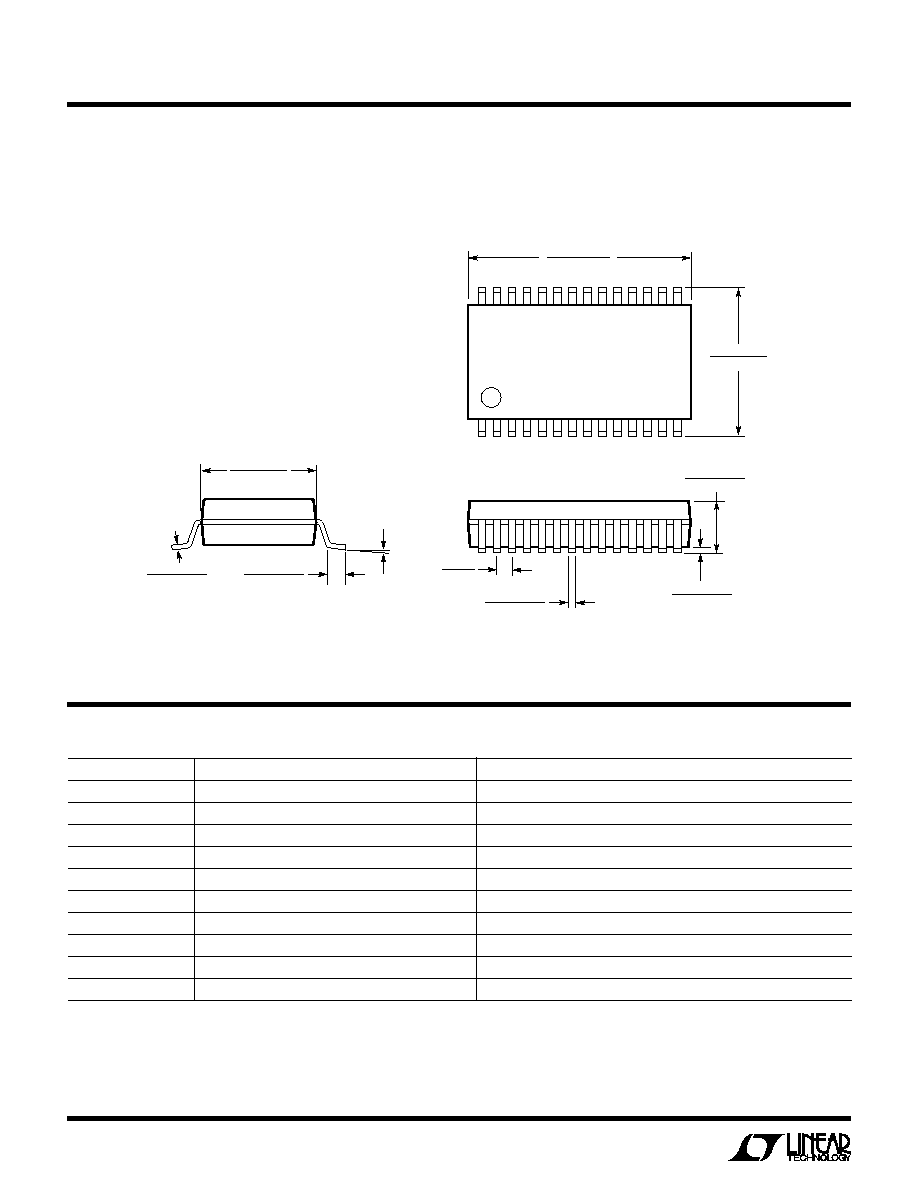
G Package
28-Lead Plastic SSOP (0.209)
(LTC DWG # 05-08-1640)
G28 SSOP 1098
0.13 ≠ 0.22
(0.005 ≠ 0.009)
0
∞
≠ 8
∞
0.55 ≠ 0.95
(0.022 ≠ 0.037)
5.20 ≠ 5.38**
(0.205 ≠ 0.212)
7.65 ≠ 7.90
(0.301 ≠ 0.311)
1
2 3
4
5
6 7 8
9 10 11 12
14
13
10.07 ≠ 10.33*
(0.397 ≠ 0.407)
25
26
22 21 20 19 18 17 16 15
23
24
27
28
1.73 ≠ 1.99
(0.068 ≠ 0.078)
0.05 ≠ 0.21
(0.002 ≠ 0.008)
0.65
(0.0256)
BSC
0.25 ≠ 0.38
(0.010 ≠ 0.015)
NOTE: DIMENSIONS ARE IN MILLIMETERS
DIMENSIONS DO NOT INCLUDE MOLD FLASH. MOLD FLASH
SHALL NOT EXCEED 0.152mm (0.006") PER SIDE
DIMENSIONS DO NOT INCLUDE INTERLEAD FLASH. INTERLEAD
FLASH SHALL NOT EXCEED 0.254mm (0.010") PER SIDE
*
**