 | ÐлекÑÑоннÑй компоненÑ: LTC1622 | СкаÑаÑÑ:  PDF PDF  ZIP ZIP |
Äîêóìåíòàöèÿ è îïèñàíèÿ www.docs.chipfind.ru
1
LTC1622
Low Input Voltage
Current Mode Step-Down
DC/DC Controller
The LTC
®
1622 is a constant frequency current mode step-
down DC/DC controller providing excellent AC and DC load
and line regulation. The device incorporates an accurate
undervoltage feature that shuts the LTC1622 down when
the input voltage falls below 2V.
The LTC1622 boasts a
±
1.9% output voltage accuracy and
consumes only 350
µ
A of quiescent current. For applica-
tions where efficiency is a prime consideration and the
load current varies from light to heavy, the LTC1622 can
be configured for Burst Mode
TM
operation. Burst Mode
operation enhances low current efficiency and extends
battery run time. Burst Mode operation is inhibited during
synchronization or when the SYNC/MODE pin is pulled low
to reduce noise and possible RF interference.
High constant operating frequency of 550kHz allows the
use of a small inductor. The device can also be synchro-
nized up to 750kHz for special applications. The high
frequency operation and the available 8-lead MSOP pack-
age create a high performance solution in an extremely
small amount of PCB area.
To further maximize the life of the battery source, the
P-channel MOSFET is turned on continuously in dropout
(100% duty cycle). In shutdown, the device draws a mere
15
µ
A.
s
1- or 2-Cell Li-Ion Powered Applications
s
Cellular Telephones
s
Wireless Modems
s
Portable Computers
s
Distributed 3.3V, 2.5V or 1.8V Power Systems
s
Scanners
s
Battery-Powered Equipment
s
High Efficiency
s
Constant Frequency 550kHz Operation
s
V
IN
Range: 2V to 10V
s
Multiampere Output Currents
s
OPTI-LOOP
TM
Compensation Minimizes C
OUT
s
Selectable, Burst Mode
Operation
s
Low Dropout Operation: 100% Duty Cycle
s
Synchronizable up to 750kHz
s
Current Mode Operation for Excellent Line and Load
Transient Response
s
Low Quiescent Current: 350
µ
A
s
Shutdown Mode Draws Only 15
µ
A Supply Current
s
±
1.9% Reference Accuracy
s
Available in 8-Lead MSOP
Burst Mode and OPTI-LOOP are a trademarks of Linear Technology Corporation.
FEATURES
DESCRIPTIO
U
APPLICATIO S
U
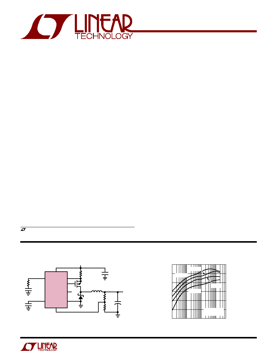
TYPICAL APPLICATIO
U
, LTC and LT are registered trademarks of Linear Technology Corporation.
Figure 1. High Efficiency Step-Down Converter
2
4
1
8
7
5
6
3
SYNC/MODE
RUN/SS
L1
4.7
µ
H
R2
0.03
D1
IR10BQ015
Si3443DV
R3
159k
V
OUT
2.5V
1.5A
R1
10k
C3
220pF
C1: TAIYO YUDEN CERAMIC EMK325BJ106MNT
C2: SANYO POSCAP 6TPA47M
D1: INTERNATIONAL RECTIFIER IR10BQ015
V
IN
2.5V TO 8.5V
R4
75k
1622 F01a
470pF
C1
10
µ
F
10V
LTC1622
V
IN
V
FB
C2
47
µ
F
6V
+
SENSE
PDRV
I
TH
GND
L1: MURATA LQN6C-4R7
R2: DALE WSL-1206 0-03
LOAD CURRENT (mA)
EFFICIENCY (%)
100
90
80
70
60
50
40
1
100
1000
5000
1622 F01b
10
V
OUT
= 2.5V
R
SENSE
= 0.03
V
IN
= 3.3V
V
IN
= 6V
V
IN
= 8.4V
V
IN
= 4.2V
Efficiency vs Load Current with
Burst Mode Operation Enabled
2
LTC1622
ABSOLUTE
M
AXI
M
U
M
RATINGS
W
W
W
U
Input Supply Voltage (V
IN
)......................... 0.3V to 10V
RUN/SS Voltage ....................................... 0.3V to 2.4V
SYNC/MODE Voltage ................................. 0.3V to V
IN
SENSE
Voltage .......................................... 2.4V to V
IN
PDRV Peak Output Current (< 10
µ
s) ......................... 1A
Storage Ambient Temperature Range ... 65
°
C to 150
°
C
Operating Temperature Range
Commercial ............................................ 0
°
C to 70
°
C
Industrial ........................................... 45
°
C to 85
°
C
Junction Temperature (Note 2) ............................. 125
°
C
Lead Temperature (Soldering, 10 sec).................. 300
°
C
PACKAGE/ORDER I
N
FOR
M
ATIO
N
W
U
U
T
JMAX
= 125
°
C,
JA
= 150
°
C/ W
S8 PART MARKING
ORDER PART
NUMBER
LTC1622CS8
LTC1622IS8
1622
1622I
ORDER PART
NUMBER
Consult factory for Military grade parts.
1
2
3
4
SENSE
I
TH
V
FB
RUN/SS
8
7
6
5
V
IN
PDRV
GND
SYNC/MODE
TOP VIEW
MS8 PACKAGE
8-LEAD PLASTIC MSOP
T
JMAX
= 125
°
C,
JA
= 250
°
C/ W
LTC1622CMS8
MS8 PART MARKING
LTDB
ELECTRICAL CHARACTERISTICS
SYMBOL
PARAMETER
CONDITIONS
MIN
TYP
MAX
UNITS
I
VFB
Feedback Current
(Note 3) V
FB
= 0.8V
10
70
nA
V
FB
Regulated Feedback Voltage
(Note 3) Commercial Grade
q
0.785
0.8
0.815
V
(Note 3) Industrial Grade
q
0.780
0.8
0.820
V
V
OVL
Output Overvoltage Lockout
Referenced to Nominal V
OUT
4
7.5
10.5
%
V
OSENSE
Reference Voltage Line Regulation
V
IN
= 4.2V to 8.5V (Note 3)
0.04
0.08
%/V
V
LOADREG
Output Voltage Load Regulation
Measured in Servo Loop; V
ITH
= 0.2V to 0.625V
0.3
0.5
%
Measured in Servo Loop; V
ITH
= 0.9V to 0.625V
0.3
0.5
%
I
S
Input DC Supply Current
(Note 4)
Burst Mode Inhibited
V
IN
= 2.3V
450
µ
A
Sleep Mode
V
ITH
= 0V, V
SYNC/MODE
= 2.4V
350
400
µ
A
Shutdown
V
RUN/SS
= 0V
15
30
µ
A
Shutdown
V
RUN/SS
= 0V, V
IN
= V
UVLO
0.1V
4
10
µ
A
V
RUN/SS
RUN/SS Threshold
Commercial Grade
q
0.4
0.7
0.9
V
Industrial Grade
q
0.3
0.7
1.0
V
I
RUN/SS
Soft-Start Current Source
V
RUN/SS
= 0V
1
2.5
5
µ
A
f
OSC
Oscillator Frequency
V
FB
= 0.8V
475
550
625
kHz
V
FB
= 0V
75
110
140
kHz
V
SYNC/MODE
SYNC/MODE Threshold
V
SYNC/MODE
Ramping Down
1
1.5
V
V
UVLO
Undervoltage Lockout
V
IN
Ramping Down
q
1.55
1.92
2.3
V
V
IN
Ramping Up
1.97
2.36
V
TOP VIEW
S8 PACKAGE
8-LEAD PLASTIC SO
1
2
3
4
8
7
6
5
SENSE
I
TH
V
FB
RUN/SS
V
IN
PDRV
GND
SYNC/MODE
(Note 1)
The
q
denotes specifications which apply over the full operating
temperature range, otherwise specifications are at T
A
= 25
°
C. V
IN
= 4.2V
3
LTC1622
ELECTRICAL CHARACTERISTICS
SYMBOL
PARAMETER
CONDITIONS
MIN
TYP
MAX
UNITS
PDRV t
r
Gate Drive Rise Time
C
LOAD
= 3000pF
80
140
ns
PDRV t
f
Gate Drive Fall Time
C
LOAD
= 3000pF
100
140
ns
V
SENSE(MAX)
Maximum Current Sense Voltage
q
80
110
140
mV
Note 1: Absolute Maximum Ratings are those values beyond which the life
of a device may be impaired.
Note 2: T
J
is calculated from the ambient temperature T
A
and power
dissipation P
D
according to the following formula:
LTC1622CS8; T
J
= T
A
+ (P
D
· 150
°
C/W),
LTC1622CMS8; T
J
= T
A
+ (P
D
· 250
°
C/W)
Note 3: The LTC1622 is tested in a feedback loop that servos V
FB
to the
feedback point for the error amplifier (V
ITH
= 0.8V).
Note 4: Dynamic supply current is higher due to the gate charge being
delivered at the switching frequency.
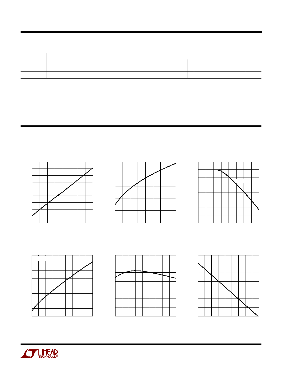
TYPICAL PERFOR
M
A
N
CE CHARACTERISTICS
U
W
SUPPLY VOLTAGE (V)
2
3
SHUTDOWN CURRENT (
µ
A)
10
1622 G01
4
5
6
7
8
9
45
40
35
30
25
20
15
10
5
0
DUTY CYCLE (%)
20
30
TRIP VOLTAGE (mV)
100
1622 G03
40
50
60
70
80
90
110
100
90
80
70
60
50
40
30
V
IN
= 4.2V
UNSYNC
TEMPERATURE (
°
C)
55 35
UNDERVOLTAGE LOCKOUT VOLTAGE (V)
125
1622 G06
15
5
25
45
65
85 105
2.10
2.05
2.00
1.95
1.90
1.85
1.80
1.75
RUN/SS Current vs Supply Voltage
SUPPLY VOLTAGE (V)
2
SOFT-START CURRENT (
µ
A)
8
1622 G02
4
6
10
3.50
3.00
2.50
2.00
1.50
1.00
3
5
7
9
TEMPERATURE (
°
C)
55 35
REFERENCE VOLTAGE (V)
125
1622 G05
15
5
25
45
65
85 105
0.810
0.805
0.800
0.795
0.790
0.785
0.780
0.775
V
IN
= 4.2V
Shutdown Current
vs Supply Voltage
Maximum Current Sense Voltage
vs Duty Cycle
Undervoltage Lockout Voltage
vs Temperature
Reference Voltage
vs Temperature
TEMPERATURE (
°
C)
55 35
NORMALIZED FREQUENCY (%)
125
1622 G04
15
5
25
45
65
85 105
10.0
7.5
5.0
2.5
0
2.5
5.0
7.5
10.0
V
IN
= 4.2V
Normalized Oscillator Frequency
vs Temperature
The
q
denotes specifications which apply over the full operating
temperature range, otherwise specifications are at T
A
= 25
°
C. V
IN
= 4.2V
4
LTC1622
TYPICAL PERFOR
M
A
N
CE CHARACTERISTICS
U
W
PI
N
FU
N
CTIO
N
S
U
U
U
SENSE
(Pin 1): The Negative Input to the Current Com-
parator.
I
TH
(Pin 2): Error Amplifier Compensation Point. The
current comparator threshold increases with this control
voltage. Nominal voltage range for this pin is 0V to 1.2V.
V
FB
(Pin 3): Receives the feedback voltage from an exter-
nal resistive divider across the output capacitor.
RUN/SS (Pin 4): Combination of Soft-Start and Run
Control Inputs. A capacitor to ground at this pin sets the
ramp time to full output current. The time is approximately
0.45s/
µ
F. Forcing this pin below 0.4V causes all circuitry
to be shut down.
SYNC/MODE (Pin 5): This pin performs three functions.
Greater than 2V on this pin allows Burst Mode operation
at low load currents, while grounding or applying a clock
signal on this pin defeats Burst Mode operation. An
external clock between 625kHz and 750kHz applied to this
pin forces the LTC1622 to operate at the external clock
frequency.
Do not attempt to synchronize below 625kHz.
Pin 5 has an internal 1
µ
A pull-up current source.
GND (Pin 6): Ground Pin.
PDRV (PIN 7): Gate Drive for the External P-Channel
MOSFET. This pin swings from 0V to V
IN
.
V
IN
(Pin 8): Main Supply Pin. Must be closely decoupled
to ground Pin 6.
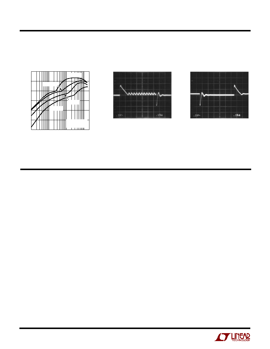
LOAD CURRENT (mA)
1
EFFICIENCY (%)
100
90
80
70
60
50
40
10
100
1622 G07
1000
V
OUT
= 2.5V
R
SENSE
= 0.03
V
IN
= 3.3V
V
IN
= 4.2V
V
IN
= 8.4V
V
IN
= 6V
Efficiency vs Load Current for
Figure 1 with Burst Mode
Operation Defeated
Load Step Transient Response
Burst Enabled
I
LOAD
= 50mA TO 1.2A
V
IN
= 4.2V
1622 G08
I
LOAD
= 50mA TO 1.2A
V
IN
= 4.2V
1622 G09
Load Step Transient Response
Burst Inhibited
100mV/DIV
100mV/DIV
5
LTC1622
FU
N
CTIO
N
AL DIAGRA
U
U
W
OPERATIO
U
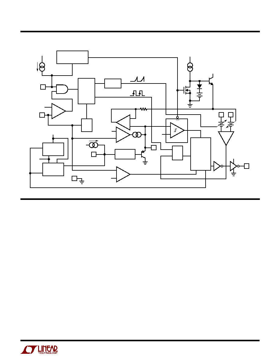
Main Control Loop
The LTC1622 is a constant frequency current mode switch-
ing regulator. During normal operation, the external
P-channel power MOSFET is turned on each cycle when
the oscillator sets the R
S
latch (R
S1
) and turned off when
the current comparator (I
COMP
) resets the latch. The peak
inductor current at which I
COMP
resets the R
S
latch is
controlled by the voltage on the I
TH
pin, which is the output
of the error amplifier EA. An external resistive divider
connected between V
OUT
and ground allows EA to receive
an output feedback voltage V
FB
. When the load current
increases, it causes a slight decrease in V
FB
relative to the
0.8V reference, which in turn causes the I
TH
voltage to
increase until the average inductor current matches the
new load current.
The main control loop is shut down by pulling the RUN/SS
pin low. Releasing RUN/SS allows an internal 2.5
µ
A
(Refer to Functional Diagram)
current source to charge up the soft-start capacitor C
SS
.
When C
SS
reaches 0.7V, the main control loop is enabled
with the I
TH
voltage clamped at approximately 5% of its
maximum value. As C
SS
continues to charge, I
TH
is gradu-
ally released allowing normal operation to resume.
Comparator OV guards against transient overshoots
> 7.5% by turning off the P-channel power MOSFET and
keeping it off until the fault is removed.
Burst Mode Operation
The LTC1622 can be enabled to go into Burst Mode
operation at low load currents simply by leaving the SYNC/
MODE pin open or connecting it to a voltage of at least 2V.
In this mode, the peak current of the inductor is set as if
V
ITH
= 0.36V (at low duty cycles) even though the voltage
at the I
TH
pin is at lower value. If the inductor's average
current is greater than the load requirement, the voltage at
+
+
+
+
+
+
BURST DEFEAT
1
µ
A
5
SYNC/
MODE
3
6
4
2
S
R
Q
BURST
R
S1
0.12V
SLEEP
SENSE
EN
1
0.36V
8
PDRV
OV
1622 BD
7
GND
V
REF
0.8V
RUN/SS
V
IN
SLOPE
COMP
Y = "0" ONLY WHEN X IS A CONSTANT "1"
OTHERWISE Y = "1"
FREQ
SHIFT
OSC
2.5
µ
A
g
m
= 0.5m
EA
SWITCHING
LOGIC
AND
BLANKING
CIRCUIT
RUN/
SOFT-START
V
REF
+ 60mV
SHUTDOWN
V
FB
0.3V
V
IN
V
IN
V
IN
V
CC
ICOMP
I
TH
X
Y
V
IN
0.8V
REFERENCE
UVLO
TRIP = 1.97V
0.8V
V
REF