1642af.pm65
1
LTC1642A
1642af
Hot Swap Controller
Adjustable Undervoltage and Overvoltage
Protection
Foldback Current Limit
Adjustable Current Limit Time-Out
V
CC
: 2.97V to 16.5V Normal Operation, Protected
Against Surges to 33V
Single Channel NFET Driver
Latch Off or Automatic Retry on Current Fault
Driver for SCR Crowbar on Overvoltage
Adjustable Reset Timer
Reference Output with Uncommitted Comparator
16-Pin SSOP Package
Hot Board Insertion
Electronic Circuit Breaker
InfiniBand
TM
Systems
1N4705
18V
12V
BACKPLANE
(SHORT PIN)
PLUG-IN CARD
V
CC
SENSE
GATE
GND BRK TMR
LTC1642A
RST TMR
ON
FAULT
OV
RESET
FB
CRWBR
COMP
+
COMP
0.33
µF
0.33
µF
2N2222
MCR
12DC
REF
0.1
µF
2.87k
1%
110k
1%
100
5%
107k
1%
13k
1%
FDS6630A
0.01
µF
0.047
µF
C
LOAD
12V
AT 2.5A
330
5%
0.010
5%
11.3k
1%
POWER-GOOD = 11.4V
1642a TA01
+
COMPOUT
GND
UV = 10.8V
OV = 13.2V
APPLICATIO S
U
FEATURES
TYPICAL APPLICATIO
U
The LTC
®
1642A is a 16-pin Hot Swap
TM
controller that
allows a board to be safely inserted and removed from a
live backplane. Using an external N-Channel pass transis-
tor, the board supply voltage can be ramped up at an
adjustable rate. A high side switch driver controls the
N-Channel gate for supply voltages ranging from 2.97V
to 16.5V.
The SENSE pin allows foldback limiting of the load current,
with circuit breaker action after an adjustable delay time.
The delay allows the part to power-up in current limit. The
CRWBR output can be used to trigger an SCR for crowbar
protection of the load if the input supply exceeds an
adjustable threshold. The RESET output can generate a
system reset with adjustable delay when the supply volt-
age falls below an adjustable threshold. The ON pin cycles
the board power. The LTC1642A is available in the 16-pin
SSOP package.
DESCRIPTIO
U
, LTC and LT are registered trademarks of Linear Technology Corporation. All other
trademarks are the property of their respective owners. Hot Swap is a trademark of Linear
Technology Corporation.
2
LTC1642A
1642af
Supply Voltage (V
CC
) ................................. 0.3V to 33V
SENSE Pin ................................... 0.3V to (V
CC
+ 0.3V)
ON, FB, OV, COMP
+
, COMP
RESET, FAULT, COMPOUT ..................... 0.3V to 18.5V
Operating Temperature Range
LTC1642AC ............................................. 0
°C to 70°C
LTC1642AI ......................................... 40
°C to 85°C
Storage Temperature Range ................. 65
°C to 150°C
Lead Temperature (Soldering, 10 sec).................. 300
°C
ABSOLUTE AXI U
RATI GS
W
W
W
U
PACKAGE/ORDER I FOR ATIO
U
U
W
(Note 1)
ORDER PART
NUMBER
LTC1642ACGN
LTC1642AIGN
Consult LTC Marketing for parts specified with wider operating temperature ranges.
T
JMAX
= 150
°C,
JA
= 130
°C/W
DC ELECTRICAL CHARACTERISTICS
SYMBOL
PARAMETER
CONDITIONS
MIN
TYP
MAX
UNITS
V
CC
Operating Voltage Range
2.97
16.5
V
I
CC
V
CC
Supply Current
ON = V
CC
1.25
3.0
mA
V
LKHI
V
CC
Undervoltage Lockout
V
CC
Rising
2.55
2.73
2.95
V
V
LKLO
V
CC
Undervoltage Lockout
V
CC
Falling
2.35
2.50
2.95
V
V
LKHYST
V
CC
Undervoltage Lockout Hysteresis
230
mV
V
FB
FB Pin Voltage Threshold
FB Falling
1.208
1.220
1.232
V
V
FB
FB Pin Threshold Supply Variation
FB Falling,
2.97V
V
CC
16.5V
5
15
mV
V
FBHST
FB Pin Voltage Threshold Hysteresis
3
mV
I
FB(IN)
FB Pin Input Current
V
OV
= 5V
0
±1
µA
V
OV
OV Pin Voltage Threshold
OV Rising
1.208
1.220
1.232
V
V
OV
OV Pin Threshold Supply Variation
OV Rising,
2.97V
V
CC
16.5V
5
15
mV
V
OVHYST
OV Pin Voltage Theshold Hysteresis
3
mV
I
OV(IN)
OV Pin Input Current
V
FB
= 5V
0
±1
µA
V
RST
RST TMR Pin Voltage Threshold
RST TMR Rising
1.200
1.220
1.250
V
V
RST
RST TMR Pin Threshold Supply Variation
RST TMR Rising, 2.97V
V
CC
16.5V
5
15
mV
I
RST
RST TMR Pin Current
Timer On
1.5
2.0
2.5
µA
Timer Off, V
RSTTMR
= 1.5V
10
mA
V
BRK
BRK TMR Pin Voltage Threshold
BRK TMR Rising
1.200
1.220
1.250
V
V
BRK
BRK TMR Pin Threshold Supply Variation
BRK TMR Rising, 2.97V
V
CC
16.5V
5
15
mV
I
BRK
BRK TMR Pin Current
Timer On
15
20
30
µA
Timer Off, V
BRKTMR
= 1.5V
10
mA
V
CR
CRWBR Pin Voltage Theshold
CRWBR Rising
375
410
425
mV
V
CR
CRWBR Pin Threshold Supply Variation
2.97V
V
CC
16.5V
4
15
mV
I
CR
CRWBR Pin Current
CRWBR On, V
CRWBR
= 0V
30
45
60
µA
CRWBR On, V
CRWBR
= 2.1V
1000
1500
µA
CRWBR Off, V
CRWBR
= 1.5V
2.3
mA
The
denotes the specifications which apply over the full operating temperature range, otherwise specifications are at T
A
= 25
°C.
V
CC
= 5V unless otherwise specified.
GN PART
MARKING
1642A
1642AI
1
2
3
4
5
6
7
8
TOP VIEW
16
15
14
13
12
11
10
9
CRWBR
BRK TMR
RST TMR
ON
RESET
FAULT
FB
GND
V
CC
SENSE
GATE
REF
COMP
COMP
+
COMPOUT
OV
GN PACKAGE
16-LEAD PLASTIC SSOP
Order Options Tape and Reel: Add #TR
Lead Free: Add #PBF Lead Free Tape and Reel: Add #TRPBF
Lead Free Part Marking:
http://www.linear.com/leadfree/
3
LTC1642A
1642af
V
CB
Circuit Breaker Trip Voltage
V
CB
= (V
CC
V
SENSE
), V
FB
= GND
15
25
36
mV
V
CB
= (V
CC
V
SENSE
), V
FB
= 1V
45
52.5
60
mV
2.97V
V
CC
16.5V,
V
CB
= (V
CC
V
SENSE
), V
FB
= GND
12
25
39
mV
V
CB
= (V
CC
V
SENSE
), V
FB
= 1V
42
52.5
63
mV
I
SENSE
SENSE Pin Input Bias Current
V
CC
= V
SENSE
= 16.5V
0.5
µA
I
GATE
GATE Pin Output Current
Charge Pump On, V
GATE
= GND
20
25
30
µA
Charge Pump Off, V
GATE
= 5V
10
mA
V
GATE
External N-Channel Gate Drive
V
GATE
V
CC,
V
CC
= 2.97V
4.5
5.9
8.0
V
V
GATE
V
CC,
V
CC
= 5V
10
11.5
14
V
V
GATE
V
CC,
V
CC
= 15V (0
°C to 70°C)
6.5
8.5
18
V
V
GATE
V
CC,
V
CC
= 15V (40
°C to 85°C)
6
8.5
18
V
V
ONHI
ON Pin Threshold
ON Rising
1.30
1.34
1.38
V
V
ONLO
ON Pin Threshold
ON Falling
1.20
1.22
1.26
V
V
ONHYST
ON Pin Hysteresis
110
mV
I
ON(IN)
ON Pin Input Current
V
ON
= 5V
0
±1
µA
V
OL
Output Low Voltage
RESET, FAULT, COMPOUT I
OL
= 1.54mA
0.4
V
RESET, FAULT I
O
= 5mA
2
V
I
PU
Logic Output Pull-Up Current
RESET, FAULT = GND
15
µA
V
REF
Reference Output Voltage
No Load
1.208
1.220
1.232
V
V
LNR
Reference Supply Variation
2.97V
V
CC
16.5V, No Load
5
15
mV
V
LDR
Reference Load Regulation
I
O
= 0mA to 1mA, Sourcing Only
2.5
7.5
mV
I
RSC
Reference Short-Circuit Current
V
REF
= 0V
4.5
mA
V
COS
Comparator Offset Voltage
V
CM
= V
REF
±10
mV
V
CHYST
Comparator Hysteresis
V
CM
= V
REF
3
mV
DC ELECTRICAL CHARACTERISTICS
The
denotes the specifications which apply over the full operating temperature range, otherwise specifications are at T
A
= 25
°C.
V
CC
= 5V unless otherwise specified.
SYMBOL
PARAMETER
CONDITIONS
MIN
TYP
MAX
UNITS
Note 1: Absolute Maximum Ratings are those values beyond which the life
of a device may be impaired.
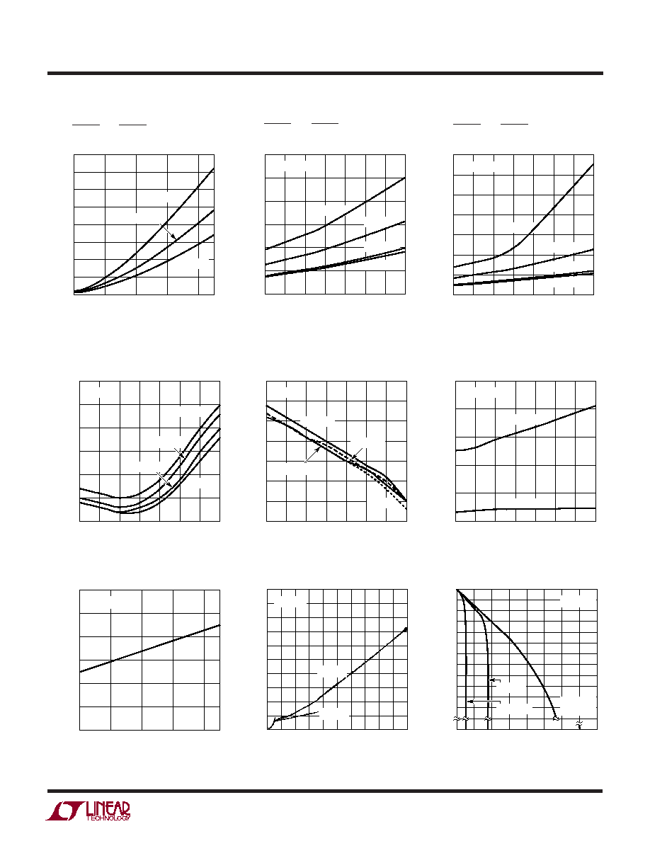
TYPICAL PERFOR A CE CHARACTERISTICS
U
W
TEMPERATURE (
°C)
50
25
0
25
50
75
100
125
V
GATE
(V)
1642a G03
16
14
12
10
8
6
4
2
0
V
CC
= 12V
V
CC
= 5V
V
CC
= 15V
V
CC
= 3V
V
GATE
vs Temperature
TEMPERATURE (
°C)
50
25
0
25
50
75
100
125
I
GATE
(
µ
A)
1642a G04
30
29
28
27
26
25
24
23
22
21
20
V
GATE
= 0V
V
CC
= 3V
V
CC
= 5V
V
CC
= 12V
V
CC
= 15V
I
GATE
vs Temperature
V
CC
(V)
3
6
9
12
15
V
GATE
(V)
1642a G26
15
12
9
6
3
0
T
A
= 25
°C
V
GATE
vs V
CC
4
LTC1642A
1642af
TYPICAL PERFOR A CE CHARACTERISTICS
U
W
TEMPERATURE (
°C)
50
25
0
25
50
75
100
125
FB THRESHOLD VOLTAGE (V)
1642a G06
1.226
1.224
1.222
1.220
1.218
1.216
1.214
V
CC
= 5V
FB FALLING
FB RISING
TEMPERATURE (
°C)
50
25
0
25
50
75
100
125
OV THRESHOLD VOLTAGE (V)
1642a G07
1.226
1.224
1.222
1.220
1.218
1.216
1.214
V
CC
= 5V
OV FALLING
OV RISING
OV Threshold Voltage vs
Temperature
FB Threshold Voltage vs
Temperature
V
CC
(V)
3
6
9
12
15
CRWBR DRIVER CURRENT (mA)
1642a G35
2.0
1.6
1.2
0.8
0.4
0
T
A
= 25
°C
CRWBR Driver Current vs V
CC
V
CC
(V)
3
6
9
12
15
FB THRESHOLD VOLTAGE (V)
1642a G27
1.232
1.228
1.224
1.220
1.216
1.212
1.208
FB RISING
FB FALLING
T
A
= 25
°C
FB Threshold Voltage vs V
CC
OV Threshold Voltage vs V
CC
V
CC
(V)
3
6
9
12
15
OV THRESHOLD VOLTAGE (V)
1642a G28
1.232
1.228
1.224
1.220
1.216
1.212
1.208
OV RISING
OV FALLING
T
A
= 25
°C
TEMPERATURE (
°C)
50
25
0
25
50
75
100
125
CRWBR DRIVER CURRENT (mA)
1642a G13
1.45
1.44
1.43
1.42
1.41
1.40
1.39
1.38
V
CC
= 5V
CRWBR Driver Current vs
Temperature
TEMPERATURE (
°C)
50
25
0
25
50
75
100
125
CRWBRTMR THRESHOLD VOLTAGE (mV)
1642a G05
405
404
403
402
401
400
399
398
397
396
395
V
CC
= 5V
CRWBR-TMR Threshold Voltage
vs Temperature
V
CC
(V)
3
6
9
12
15
I
GATE
(
µ
A)
1642a G23
25
20
15
10
5
0
V
GATE
= 0V
T
A
= 25
°C
I
GATE
Pull-Up Current vs V
CC
V
GATE
(V)
0
4
8
12
16
20
24
I
GATE
(A)
1642a G36
128
112
96
80
64
48
32
16
0
V
CC
= 12V
T
A
= 25
°C
V
CC
= 3.3V
V
CC
= 5V
GATE Pull-Down Current (Current
Limit Active)
5
LTC1642A
1642af
V
CC
(V)
0
25
50
I
CC
(mA)
1642a G25
20
10
0
V
ON
= 5V
T
A
= 25
°C
V
ON
= 0V
TYPICAL PERFOR A CE CHARACTERISTICS
U
W
I
CC
vs V
CC
ON Pin Threshold Voltage vs
Temperature
TEMPERATURE (
°C)
50
25
0
25
50
75
100
125
ON PIN THRESHOLD VOLTAGE (V)
1642a G22
1.40
1.36
1.32
1.28
1.24
1.20
V
CC
= 12V
ON RISING
ON FALLING
V
CC
(V)
3
6
9
12
15
V
REF
(V)
1642a G24
1.232
1.228
1.224
1.220
1.216
1.212
1.208
T
A
= 25
°C
V
REF
vs V
CC
V
CC
(V)
3
6
9
12
15
PULL-UP CURRENT (
µ
A)
1642a G14
160
140
120
100
80
60
40
20
0
T
A
= 55
°C
T
A
= 125
°C
T
A
= 25
°C
TEMPERATURE (
°C)
50
25
0
25
50
75
100
125
VOLTAGE (mV)
1642a G16
600
500
400
300
200
100
0
V
CC
= 12V
V
CC
= 5V
V
CC
= 15V
V
CC
= 3V
I
OL
= 1.54mA
TEMPERATURE (
°C)
50
25
0
25
50
75
100
125
VOLTAGE (V)
1642a G17
3.5
3.0
2.5
2.0
1.5
1.0
0.5
0
V
CC
= 12V
V
CC
= 5V
V
CC
= 15V
V
CC
= 3V
I
OL
= 5mA
TEMPERATURE (
°C)
50
25
0
25
50
75
100
125
CURRENT LIMIT THRESHOLD VOLTAGE (mV)
1642a G20
27.5
27.0
26.5
26.0
25.5
25.0
24.5
V
CC
= 3V
FB = 0V
V
CC
= 15V
V
CC
= 12V
V
CC
= 5V
FAULT and RESET Pull-Up Current
(I
OH
) vs V
CC
FAULT and RESET V
OL
vs
Temperature
FAULT and RESET V
OL
vs
Temperature
Current Limit Threshold Voltage
(Full Foldback) vs Temperature
Current Limit Threshold Voltage
(Nominal) vs Temperature
TEMPERATURE (
°C)
50
25
0
25
50
75
100
125
CURRENT LIMIT THRESHOLD VOLTAGE (mV)
1642a G21
57.0
56.5
56.0
55.5
55.0
54.5
54.0
53.5
V
CC
= 3V
FB = 1V
V
CC
= 15V
V
CC
= 5V
V
CC
= 12V
Reference O/P Impedance
I
REF
(mA)
0
2.5
5
7.5
10
12.5
15
17.5
20
V
REF
(mV)
1642a G37
0
2
4
6
8
10
12
14
16
18
20
22
42
V
CC
= 12V,
15V
T
A
= 25
°C
V
CC
= 5V
V
CC
= 3.3V