1
LTC1643AL
LTC1643AL-1/LTC1643AH
1643afa
PCI-Bus Hot Swap
Controller
Hot Swappable PCI Supply
s
Allows Safe Board Insertion and Removal from a
Live PCI Slot
s
Works on either a Motherboard (LTC1643AH) or
CompactPCI
TM
Card (LTC1643AL/LTC1643AL-1)
s
Controls ≠12V, 3.3V, 5V, 12V Supplies
s
Programmable Foldback Current Limit with
Circuit Breaker
s
User-Programmable Supply Voltage Power-Up Rate
s
High Side Drive for External N-Channel MOSFETs
s
≠12V and 12V On-Chip Switches
s
Fault and Power-Good Outputs
s
Available in a Narrow 16-Lead SSOP Package
The LTC
Æ
1643A is a Hot Swap
TM
controller that allows a board
to be safely inserted and removed from a live PCI-Bus slot.
Two external N-channel transistors control the 3.3V and 5V
supplies while on-chip switches control the ≠12V and 12V
supplies. All supply voltages can be ramped up at a program-
mable rate. An electronic circuit breaker protects all four
supplies against overcurrent faults. The foldback current limit
feature limits current spikes and power dissipation when
shorts occur and allows boards with large capacitances to be
powered up without tripping the circuit breaker. The PWRGD
output indicates when all of the supply voltages are within
tolerance and the FAULT output indicates an overcurrent
condition. The ON(LTC1643AH)/ON (LTC1643AL/
LTC1643AL-1) pin is used to cycle the board power or reset
the circuit breaker. The LTC1643AL-1 has the
±
12V power
good comparators disabled.
The LTC1643A is available in a 16-pin narrow SSOP package.
s
PCI-Based Servers
s
CompactPCI
Compliant Boards
, LTC and LT are registered trademarks of Linear Technology Corporation.
Hot Swap is a trademark of Linear Technology Corporation.
CompactPCI is a trademark of PCI Industrial Computer Manufacturing Group.
FEATURES
DESCRIPTIO
U
APPLICATIO S
U
TYPICAL APPLICATIO
N
U
R2
0.005
Q2
IRF7413
Q1
IRF7413
R1
0.007
R5
10
R6
10
R7
100
C1
0.047
µ
F
5V
5A
3.3V
7.6A
GND
≠12V
100mA
12V
500mA
R3
10k
R4
10k
11
3
13
12
14
16
15
4
10
9
8
1
2
5
6
7
3V
IN
GND
12V
IN
V
EEIN
ON
FAULT
PWRGD
3V
SENSE
5V
SENSE
3V
OUT
LTC1643AH
5V
OUT
12V
OUT
V
EEOUT
TIMER
5V
IN
GATE
1643A TA01
SYSTEM
POWER
SUPPLY
PCI
POWER
SYSTEM
CONTROLLER
C2
0.1
µ
F
RESET
LOGIC
RESET
2
LTC1643AL
LTC1643AL-1/LTC1643AH
1643afa
ABSOLUTE
M
AXI
M
U
M
RATINGS
W
W
W
U
PACKAGE/ORDER I
N
FOR
M
ATIO
N
W
U
U
ORDER PART NUMBER
(Note 1)
Supply Voltages
12V
IN
................................................................ 13.2V
V
EEIN
.............................................................. ≠13.2V
Input Voltage (Pin 5) ................ ≠ 0.3V
to (12V
IN
+ 0.3V)
Output Voltages (Pins 6, 7) ...... ≠ 0.3V
to (12V
IN
+ 0.3V)
Analog Voltages
(Pins 3, 4, 9, 10 to 14) ........ ≠ 0.3V
to (12V
IN
+ 0.3V)
V
EEOUT
............................................ ≠13.2V to + 0.3V
12V
OUT
.............................................. ≠ 0.3V to 13.2V
Operating Temperature Range
LTC1643ALC/LTC1643AL-1C/
LTC1643AHC ........................................... 0
∞
C to 70
∞
C
LTC1643ALI/LTC1643AL-1I/
LTC1643AHI ...................................... ≠ 40
∞
C to 85
∞
C
Storage Temperature Range ................. ≠ 65
∞
C to 150
∞
C
Lead Temperature (Soldering, 10 sec).................. 300
∞
C
TOP VIEW
GN PACKAGE
16-LEAD NARROW PLASTIC SSOP
1
2
3
4
5
6
7
8
16
15
14
13
12
11
10
9
12V
IN
V
EEIN
3V
OUT
TIMER
ON/ON*
FAULT
PWRGD
GND
12V
OUT
V
EEOUT
5V
OUT
5V
IN
5V
SENSE
GATE
3V
SENSE
3V
IN
*ON FOR LTC1643AH,
ON FOR LTC1643AL/LTC1643AL-1
T
JMAX
= 150
∞
C,
JA
= 135
∞
C/ W
Consult LTC Marketing for parts specified with wider operating temperature ranges.
LTC1643AHCGN
LTC1643ALCGN
LTC1643AL-1CGN
LTC1643AHIGN
LTC1643ALIGN
LTC1643AL-1IGN
DC ELECTRICAL CHARACTERISTICS
SYMBOL
PARAMETER
CONDITIONS
MIN
TYP
MAX
UNITS
I
DD
V
12VIN
Supply Current
ON = GND, ON = 3V
q
3.5
8
mA
V
LKO
Undervoltage Lockout
12V
IN
q
7
9.5
10.8
V
3V
IN
q
2.25
2.5
2.75
V
5V
IN
q
2.25
2.5
2.75
V
V
FB
Foldback Current Limit Voltage
V
FB
= (V
5VIN
≠ V
5VSENSE
), V
5VOUT
= 0V
q
4
7.5
12
mV
V
FB
= (V
5VIN
≠ V
5VSENSE
), V
5VOUT
> 4V
q
40
53
65
mV
V
FB
= (V
3VIN
≠ V
3VSENSE
), V
3VOUT
= 0V
q
4
7.5
12
mV
V
FB
= (V
3VIN
≠ V
3VSENSE
), V
3VOUT
> 2V
q
40
53
65
mV
t
CB
Circuit Breaker Trip Filter Time
14.6
µ
s
I
CP
GATE Pin Output Current
Charge Pump On, V
GATE
= GND, FAULT = High
q
≠ 20
≠ 62
≠ 100
µ
A
Charge Pump Off, V
GATE
= 5V, FAULT = High
200
µ
A
Charge Pump Off, V
GATE
= 2V, FAULT = Low
q
3
17.5
mA
V
GATE
External Gate Voltage
(V
12VIN
≠ V
GATE
)
100
200
mV
V
DROP
Internal Switch Voltage Drop
(V
12VIN
≠ V
12VOUT
),
0
∞
C
T
A
70
∞
C
q
225
600
I
12VOUT
= 500mA
≠ 40
∞
C
T
A
85
∞
C
q
225
750
mV
(V
EEOUT
≠ V
EEIN
), I
VEEIN
= 100mA
q
125
250
mV
I
CL
Current Foldback
12V
IN
= 12V, 12V
OUT
= 0V
q
50
250
600
mA
12V
IN
= 12V, 12V
OUT
= 10V
q
525
850
1500
mA
V
EEIN
= ≠12V, V
EEOUT
= 0V (LTC1643AL/LTC1643AH Only)
q
50
160
500
mA
V
EEIN
= ≠12V, V
EEOUT
= ≠ 10V
q
225
450
800
mA
T
TS
Thermal Shutdown Temperature
150
∞
C
V
TH
Power-Good Threshold Voltage
V
12VOUT
0
∞
C
T
A
70
∞
C
q
10.8
11.1
11.4
V
LTC1643AH/LTC1643AL Only
≠ 40
∞
C
T
A
85
∞
C
q
10.4
11.1
11.4
V
V
EEOUT
0
∞
C
T
A
70
∞
C
q
≠ 10.2
≠ 10.5
≠ 10.8
V
LTC1643AH/LTC1643AL Only
≠ 40
∞
C
T
A
85
∞
C
q
≠ 10.0
≠ 10.5
≠ 10.8
V
The
q
denotes specifications which apply over the full operating
temperature range, otherwise specifications are TA = 25
∞
C. V
12VIN
= 12V, V
EEIN
= ≠ 12V, V
3VIN
= 3.3V, V
5VIN
= 5V (Note 2)
GN PART MARKING
1643AH
1643AL
643AL1
643AHI
643ALI
43AL1I
3
LTC1643AL
LTC1643AL-1/LTC1643AH
1643afa
DC ELECTRICAL CHARACTERISTICS
TYPICAL PERFOR
M
A
N
CE CHARACTERISTICS
U
W
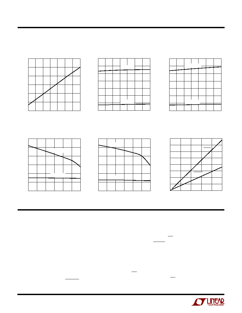
3.3V and 5V Current
Foldback Profile
OUTPUT VOLTAGE (V)
0
OUTPUT CURRENT (A)
11
10
9
8
7
6
5
4
3
2
1
0
4
1643A G01
1
2
3
5
R
SENSE
= 0.005
3V
OUT
5V
OUT
OUTPUT VOLTAGE (V)
0
OUTPUT CURRENT (A)
1.0
0.5
0
≠8
≠10
1643A G03
≠2
≠4
≠6
≠12
OUTPUT VOLTAGE (V)
0
OUTPUT CURRENT (A)
1.0
0.5
0
8
10
1643A G02
2
4
6
12
12V Current Foldback Profile
≠ 12V Current Foldback Profile
SYMBOL
PARAMETER
CONDITIONS
MIN
TYP
MAX
UNITS
V
TH
Power-Good Threshold Voltage
V
3VOUT
0
∞
C
T
A
70
∞
C
q
2.8
2.9
3.0
V
≠ 40
∞
C
T
A
85
∞
C
q
2.75
2.9
3.0
V
V
5VOUT
0
∞
C
T
A
70
∞
C
q
4.5
4.65
4.75
V
≠ 40
∞
C
T
A
85
∞
C
q
4.4
4.65
4.75
V
V
IL
Input Low Voltage
ON/ON, FAULT
q
0.8
V
V
IH
Input High Voltage
ON/ON, FAULT
q
2
V
V
OL
Output Low Voltage
FAULT, PWRGD, I = 3mA
q
0.4
V
I
IN
ON/ON Pin Input Current
ON/ON = GND
q
±
0.08
±
10
µ
A
ON/ON= 12V
IN
q
±
0.08
±
10
µ
A
5V
SENSE
Input Current
5V
SENSE
= 5V
q
50
100
µ
A
3V
SENSE
Input Current
3V
SENSE
= 3V
q
50
100
µ
A
5V
IN
Input Current
5V
IN
= 5V
q
460
700
µ
A
3V
IN
Input Current
3V
IN
= 3V
q
320
600
µ
A
5V
OUT
Input Current
5V
OUT
= 5V, ON = 3V, ON = GND
q
240
500
µ
A
3V
OUT
Input Current
3V
OUT
= 3.3V, ON = 3V, ON = GND
q
220
500
µ
A
R
DIS
5V
OUT
Discharge Impedance
ON = GND or ON = 3V
100
3V
OUT
Discharge Impedance
ON = GND or ON = 3V
70
12V
OUT
Discharge Impedance
ON = GND or ON = 3V
450
V
EEOUT
Discharge Impedance
ON = GND or ON = 3V
1600
I
TIMER
TIMER Pin Current
Timer On, V
TIMER
= GND
q
≠ 15
≠ 22
≠ 27
µ
A
Timer Off, V
TIMER
= 5V
45
mA
V
TIMER
TIMER Threshold Voltage
(V
12VIN
≠ V
TIMER
)
q
0.5
0.9
1.3
V
Note 2: All currents into device pins are positive; all currents out of device
pins are negative. All voltages are referenced to ground unless otherwise
specified.
Note 1: Absolute Maximum Ratings are those values beyond which the life
of a device may be impaired.
The
q
denotes specifications which apply over the full operating temperature range, otherwise specifications are TA = 25
∞
C.
V
12VIN
= 12V, V
EEIN
= ≠ 12V, V
3VIN
= 3.3V, V
5VIN
= 5V (Note 2)

4
LTC1643AL
LTC1643AL-1/LTC1643AH
1643afa
TYPICAL PERFOR
M
A
N
CE CHARACTERISTICS
U
W
TEMPERATURE (
∞
C)
≠50
TIMER CURRENT (
µ
A)
100
1643A G04
0
50
23.5
23.0
22.5
22.0
21.5
21.0
20.5
20.0
19.5
≠25
25
75
125
Timer Current vs Temperature
TEMPERATURE (
∞
C)
≠50
GATE I
SINK
(mA)
25.0
22.5
20.0
17.5
15.0
12.5
10.0
25
75
1643A G05
≠25
0
50
100
125
FAULT = LOW
Gate I
SINK
vs Temperature
TEMPERATURE (
∞
C)
≠50
GATE CURRENT (
µ
A)
90
80
70
60
50
40
0
50
75
1643A G06
≠25
25
100
125
Gate Current vs Temperature
Power Good Threshold Voltage vs
Temperature (12V
OUT
)
TEMPERATURE (
∞
C)
≠50
POWER GOOD THRESHOLD VOLTAGE (V)
11.14
11.12
11.10
11.08
11.06
11.04
0
50
75
1643A G07
≠25
25
100
125
Power Good Threshold Voltage vs
Temperature (5V
OUT
)
TEMPERATURE (
∞
C)
≠50
POWER GOOD THRESHOLD VOLTAGE (V)
4.68
4.67
4.66
4.65
4.64
4.63
4.62
25
75
1643A G08
≠25
0
50
100
125
TEMPERATURE (
∞
C)
≠50
POWER GOOD THRESHOLD VOLTAGE (V)
100
1643A G09
0
50
2.904
2.903
2.902
2.901
2.900
2.899
2.898
2.897
2.896
≠25
25
75
125
Power Good Threshold Voltage vs
Temperature (3V
OUT
)
Power Good Threshold Voltage
vs Temperature (V
EEOUT
)
TEMPERATURE (
∞
C)
≠50
POWER GOOD THRESHOLD VOLTAGE (V)
100
1643A G10
0
50
≠10.58
≠10.56
≠10.54
≠10.52
≠10.50
≠10.48
≠10.46
≠10.44
≠10.42
≠25
25
75
125
12V Internal Switch Voltage Drop
vs Temperature
TEMPERATURE (
∞
C)
325
300
275
250
225
200
175
150
LT
1643A G11
INTERNAL SWITCH VOLTAGE DROP (mV)
≠50
25
75
≠25
0
50
100
125
I
12VOUT
= 500mA
V
EE
Internal Switch Voltage Drop
vs Temperature
TEMPERATURE (
∞
C)
≠50
INTERNAL SWITCH VOLTAGE DROP (mV)
180
160
140
120
100
80
60
25
75
1643A G12
≠25
0
50
100
125
I
VEEIN
= 100mA
5
LTC1643AL
LTC1643AL-1/LTC1643AH
1643afa
TYPICAL PERFOR
M
A
N
CE CHARACTERISTICS
U
W
TEMPERATURE (
∞
C)
≠50
CIRCUIT BREAKER TRIP FILTER TIME (
µ
s)
15.50
15.25
15.00
14.75
14.50
14.25
14.00
25
75
1643A G13
≠25
0
50
100
125
Circuit Breaker Trip Filter Time
vs Temperature
Timer Threshold Voltage
vs Temperature
TEMPERATURE (
∞
C)
≠50
TIMER THRESHOLD VOLTAGE (V)
1.0
0.9
0.8
0.7
25
75
1643A G14
≠25
0
50
100
125
V
12VIN
≠ V
TIMER
12V
IN
Supply Current
vs Temperature
TEMPERATURE (
∞
C)
≠50
12V
IN
SUPPLY CURRENT (mA)
3.72
3.70
3.68
3.66
3.64
3.62
0
50
75
1643A G15
≠25
25
100
125
V
EEIN
Supply Current
vs Temperature
5V
IN
Supply Current
vs Temperature
TEMPERATURE (
∞
C)
≠50
V
EEIN
SUPPLY CURRENT (mA)
0.90
0.89
0.88
0.87
0.86
0.85
0.84
25
75
1643A G16
≠25
0
50
100
125
TEMPERATURE (
∞
C)
270
268
266
264
262
260
258
256
LT
1643A G17
5V
IN
SUPPLY CURRENT (
µ
A)
≠50
25
75
≠25
0
50
100
125
3V
IN
Supply Current
vs Temperature
TEMPERATURE (
∞
C)
≠50
3V
IN
SUPPLY CURRENT (
µ
A)
275.0
272.5
270.0
267.5
265.0
262.5
260.0
25
75
1643A G18
≠25
0
50
100
125
V
OL
vs Temperature
TEMPERATURE (
∞
C)
≠50
V
OL
(mV)
350
300
250
200
150
100
50
25
75
1643A G19
≠25
0
50
100
125
I = 3mA
FAULT
PWRGD
TEMPERATURE (
∞
C)
≠50
UNDERVOLTAGE LOCKOUT (V)
9.515
9.510
9.505
9.500
9.495
9.490
9.485
25
75
1643A G20
≠25
0
50
100
125
12V
IN
Undervoltage Lockout
vs Temperature
TEMPERATURE (
∞
C)
≠50
UNDERVOLTAGE LOCKOUT (V)
2.454
2.452
2.450
2.448
2.446
2.444
2.442
25
75
1643A G21
≠25
0
50
100
125
5V
IN
Undervoltage Lockout
vs Temperature
6
LTC1643AL
LTC1643AL-1/LTC1643AH
1643afa
TYPICAL PERFOR
M
A
N
CE CHARACTERISTICS
U
W
V
EE
Current Foldback
vs Temperature
I
SINK
(mA)
0
V
OL
(mV)
6
10
1643A G27
2
4
8
800
700
600
500
400
300
200
100
0
FAULT
PWRGD
V
OL
vs I
SINK
(25
∞
C)
TIMER (Pin 4): Analog Current Fault Inhibit Timing Input.
Connect a capacitor from TIMER to GND. With the chip
turned off (ON = GND or ON = High) or the internal circuit
breaker tripped (FAULT = GND), the TIMER pin is internally
held at GND. When the chip is turned on, a 22
µ
A pull-up
current source is connected to TIMER. Current limit faults
will be ignored until the voltage at the TIMER pin rises to
within 0.9V of 12V
IN
.
ON/ON (Pin 5): Digital Input.The LTC1643AL/LTC1643AL-1
have an active low enable, ON, and the LTC1643AH has an
active high enable, ON. When the ON pin is pulled high or
PI
N
FU
N
CTIO
N
S
U
U
U
12V
IN
(Pin 1): 12V Supply Input. It powers all the chip's
internal circuitry. A 0.5
switch is connected between
12V
IN
and 12V
OUT
with a foldback current limit. An under-
voltage lockout circuit prevents the switches from turning
on while the 12V
IN
pin voltage is less than 9.5V typically.
V
EEIN
(Pin 2): ≠ 12V Supply Input. A 1.2
switch is
connected between V
EEIN
and V
EEOUT
with a foldback
current limit.
3V
OUT
(Pin 3): Analog Input. Used to monitor the 3.3V
output supply voltage. The PWRGD signal cannot go high
until the 3V
OUT
pin exceeds 2.9V typically.
TEMPERATURE (
∞
C)
70
60
50
40
30
20
10
0
1643A G24
FOLDBACK CURRENT LIMIT VOLTAGE (mV)
≠50
25
75
≠25
0
50
100
125
3V
OUT
= 3.3V
3V
OUT
= 0V
3V
IN
Foldback Current Limit
Voltage vs Temperature
TEMPERATURE (
∞
C)
≠50
UNDERVOLTAGE LOCKOUT (V)
2.454
2.452
2.450
2.448
2.446
2.444
2.442
25
75
1643A G21
≠25
0
50
100
125
3V
IN
Undervoltage Lockout
vs Temperature
TEMPERATURE (
∞
C)
70
60
50
40
30
20
10
0
1643A G23
FOLDBACK CURRENT LIMIT VOLTAGE (mV)
≠50
25
75
≠25
0
50
100
125
5V
OUT
= 5V
5V
OUT
= 0V
5V
IN
Foldback Current Limit
Voltage vs Temperature
12V
Current Foldback
vs Temperature
TEMPERATURE (
∞
C)
≠50
CURRENT FOLDBACK (mA)
1200
1000
800
600
400
200
0
25
75
1643A G26
≠25
0
50
100
12V
OUT
= 12V
12V
OUT
= 0V
TEMPERATURE (
∞
C)
≠50
CURRENT FOLDBACK (mA)
600
500
400
300
200
100
0
25
75
1643A G25
≠25
0
50
100
V
EEOUT
= ≠12V
V
EEOUT
= 0V

7
LTC1643AL
LTC1643AL-1/LTC1643AH
1643afa
3V
SENSE
(Pin 10): The 3.3V Current Limit Set Pin. With a
sense resistor placed in the supply path between 3V
IN
and
3V
SENSE
, the GATE pin voltage will be adjusted to maintain
a constant voltage across the sense resistor and a con-
stant current through the switch. A foldback feature makes
the current limit decrease as the voltage at the 3V
OUT
pin
approaches GND. To disable the current limit, 3V
SENSE
and 3V
IN
can be shorted together.
GATE (Pin 11): High Side Gate Drive for the External
N-Channel Pass Transistors. Requires an external series
RC network for the current limit loop compensation and
setting the minimum ramp-up rate. During power-up, the
slope of the voltage rise at the GATE is set by the 62
µ
A
current source connected to 12V
IN
and the external ca-
pacitor connected to GND or by the 3.3V or 5V current limit
and the bulk capacitance on the 3V
OUT
or 5V
OUT
suppy
lines. During power-down, the slope of the falling voltage
is set by the 200
µ
A current source connected to GND and
the external GATE capacitor.
The voltage at the GATE pin will be modulated to maintain
a constant current when either the 3V or 5V supplies go
into current limit. When a current limit fault occurs after
the inhibit period set by the TIMER pin capacitance, the
undervoltage lockout circuit on 3.3V, 5V or 12V trips or
the FAULT pin is pulled low, the GATE pin is immediately
pulled to GND.
5V
SENSE
(Pin 12): 5V Current Limit Set Pin. With a sense
resistor placed in the supply path between 5V
IN
and
5V
SENSE
, the GATE pin voltage will be adjusted to maintain
a constant voltage across the sense resistor and a con-
stant current through the switch. A foldback feature makes
the current limit decrease as the voltage at the 5V
OUT
pin
approaches GND. To disable the current limit, 5V
SENSE
and 5V
IN
can be shorted together.
5V
IN
(Pin 13): Analog Input. Used to monitor the 5V input
supply voltage. An undervoltage lockout circuit prevents
the switches from turning on when the voltage at the 5V
IN
pin is less than 2.5V typically.
5V
OUT
(Pin 14): Analog Input. Used to monitor the 5V
output supply voltage. The PWRGD signal cannot go high
until the 5V
OUT
pin exceeds 4.65V typically.
the ON pin pulled low, the GATE pin is pulled high by a
62
µ
A current source and the internal 12V and ≠ 12V
switches are turned on. When the ON pin is pulled low or
the ON pin pulled high, the GATE pin will be pulled to
ground by a 200
µ
A current source and the 12V and ≠ 12V
switches turned off.
The ON/ON pin is also used to reset the electronic circuit
breaker. If the ON/ON pin is cycled following the trip of the
circuit breaker, the circuit breaker is reset and a normal
power-up sequence will occur.
FAULT (Pin 6): Open-Drain Digital I/O. FAULT is pulled low
when a current limit fault is detected. Current limit faults
are ignored while the voltage at the TIMER pin is less than
12V
IN
≠ 0.9V. Once the TIMER cycle is complete, FAULT
will pull low typically 14.6
µ
s after any of the supplies go
into current limit. At the same time, the GATE and TIMER
pins are pulled to GND and the 12V and ≠12V switches are
turned off. The chip will remain latched in the off state until
the ON/ON pin is toggled or the power is cycled.
Forcing the FAULT pin low with an external pull-down will
immediately turn off the internal switches and force the
GATE and TIMER pins to GND independent of the state of
the ON/ON pin. However, the chip is not latched into the off
state, so when the FAULT pin is released, the state of the
chip will be determined by the ON pin.
PWRGD (Pin 7): Open-Drain Digital Power-Good Output.
PWRGD remains low while V
12VOUT
11.4V, V
3VOUT
3V,
V
5VOUT
4.75V and V
EEOUT
≠ 10.8V. The LTC1643AL-1
has the power good comparators connected to the 12V
OUT
and V
EEOUT
pins disabled, with only the 3V
OUT
and 5V
OUT
outputs being monitored to generate PWRGD. When one
of the supplies falls below its power-good threshold
voltage, PWRGD will go high after a 15
µ
s deglitching time.
The switches will
not be turned off when PWRGD goes
high.
GND (Pin 8): Chip Ground.
3V
IN
(Pin 9): 3.3V Supply Sense Input. An undervoltage
lockout circuit prevents the switches from turning on
when the voltage at the 3V
IN
pin is less than 2.5V typically.
If no 3.3V input supply is available, tie 3V
IN
to the 5V
IN
pin.
PI
N
FU
N
CTIO
N
S
U
U
U

8
LTC1643AL
LTC1643AL-1/LTC1643AH
1643afa
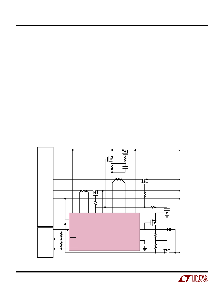
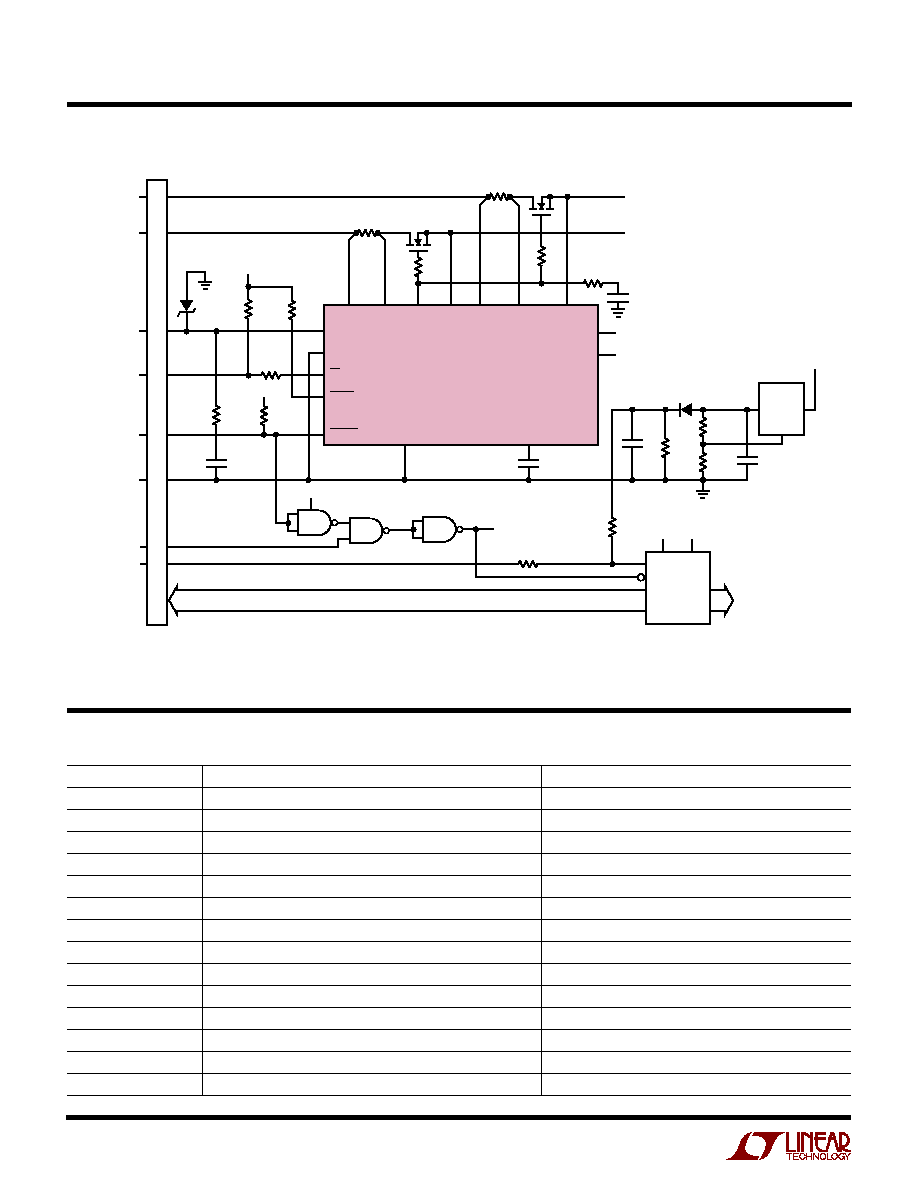
BLOCK DIAGRA
M
W
+
≠
+
≠
+
≠
+
≠
LOGIC
9.5V
UVL
5V
OUT
+
≠
3V
OUT
12V
IN
62
µ
A
200
µ
A
Q5
ON/ON
FAULT
22
µ
A
3V
SENSE
GATE
5V
IN
5V
SENSE
12V
IN
12V
OUT
V
EEIN
V
EEOUT
TIMER
GND
12V
IN
3V
IN
5V
OUT
3V
OUT
2.5V
UVL
2.5V
UVL
REF
REF
REF
LTC1643AH/LTC1643AL
ONLY
LTC1643AH/LTC1643AL
ONLY
Q2
Q8
REF
1643A BD
C
P3
+
≠
+
≠
+
≠
C
P4
C
P5
C
P7
Q3
Q4
5
13
1
16
4
2
15
8
12
11
10
9
3
14
6
7
PWRGD
Q7
Q1
Q9
Q10
Q6
APPLICATIO
N
S I
N
FOR
M
ATIO
N
W
U
U
U
Hot Circuit Insertion
When a circuit board is inserted into a live PCI slot, the
supply bypass capacitors on the board can draw huge
transient currents from the PCI power bus as they charge
up. The transient currents can cause permanent damage
to the connector pins and cause glitches on the power bus,
causing other boards in the system to reset.
The LTC1643A is designed to turn a board's supply
voltages on and off in a controlled manner, allowing the
board to be safely inserted or removed from a live PCI slot
without glitching the system power supplies. The chip
also protects the PCI supplies from shorts and monitors
the supply voltages.
The LTC1643AH is designed for motherboard applica-
tions, while the LTC1643AL/LTC1643AL-1 are designed
for CompactPCI applications where the chip resides on
the plug-in board.
V
EEOUT
(Pin 15): ≠12V Supply Output. A 1.2
switch is
connected between V
EEIN
and V
EEOUT
. V
EEOUT
must
exceed ≠10.8V before the PWRGD signal can go high on
the LTC1643AH and LTC1643AL.
PI
N
FU
N
CTIO
N
S
U
U
U
12V
OUT
(Pin 16): 12V Supply Output. A 0.5
switch is
connected between 12V
IN
and 12V
OUT
. 12V
OUT
must
exceed 11.4V before the PWRGD signal can go high on the
LTC1643AH and LTC1643AL.
9
LTC1643AL
LTC1643AL-1/LTC1643AH
1643afa
LTC1643A FEATURE SUMMARY
1. Allows safe board insertion and removal from either a
motherboard (LTC1643AH) or CompactPCI board
(LTC1643AL/LTC1643AL-1).
2. Controls all four PCI supplies: ≠12V, 12V, 3.3V and 5V.
3. Programmable foldback current limit: a programmable
analog current limit with a value that depends on the
output voltage. If the output is shorted to ground, the
current limit drops to keep power dissipation and
supply glitches to a minimum.
4. Programmable circuit breaker: if a supply remains in
current limit too long, the circuit breaker will trip, the
supplies will be turned off and the FAULT pin pulled low.
5. Current limit power-up: the supplies are allowed to
power up in current limit. Allows the chip to power up
boards with widely varying capacitive loads without
tripping the circuit breaker. The maximum allowable
power-up time is programmable using the TIMER pin.
6. ≠12V and 12V power switches on chip.
7. Power good output: monitors the voltage status of the
four supply voltages, except the LTC1643AL-1 which
only monitors 3V
OUT
and 5V
OUT
.
8. Space saving 16-pin SSOP package.
PCI Power Requirements
PCI systems usually require four power rails: 5V, 3.3V,
12V and ≠12V. Systems implementing the 3.3V signaling
environment are usually required to provide all four rails in
every system. Systems implementing the 5V signaling
environment may either ship the 3.3V supply with the
system or provide a means to add it afterward. The
tolerance of the supplies as measured at the components
on the plug-in card is summarized in Table 1.
APPLICATIO
N
S I
N
FOR
M
ATIO
N
W
U
U
U
Some
±
12V supplies in CompactPCI applications are not
well regulated and can violate the tolerance specification.
For these applications, the LTC1643AL-1 should be used
because the PWRGD signal does not depend on
±
12V
outputs.
Power-Up Sequence
The power supplies are controlled by placing external
N-channel pass transistors in the 3.3V and 5V power
paths, and internal pass transistors for the 12V and ≠12V
power paths (Figure 1).
Resistors R1 and R2 provide current fault detection and
R7 and C1 provide current control loop compensation.
Resistors R5 and R6 prevent high frequency oscillations
in Q1 and Q2.
When the ON pin (Pin 5) is pulled high, the pass transistors
are allowed to turn on and a 22
µ
A current source is
connected to the TIMER pin (Pin 4) (Figure 2).
The current in each pass transistor increases until it
reaches the current limit for each supply. Each supply is
then allowed to power up at the rate dv/dt = 62
µ
A/C1 or as
determined by the current limit and the load capacitance
whichever is slower. Current limit faults are ignored while
the TIMER pin (Pin 4) voltage is ramping up and is less
than 0.9V below 12V
IN
(Pin 1). Once all four supply
voltages are within tolerance, the PWRGD pin (Pin 7) will
pull low.
Power-Down Sequence
When the ON pin (Pin 5) is pulled low, a power-down
sequence begins (Figure 3).
Internal switches are connected to each of the output
supply voltage pins to discharge the bypass capacitors to
ground. The TIMER pin (Pin 4) is immediately pulled low.
The GATE pin (Pin 11) is pulled down by a 200
µ
A current
source to prevent the load currents on the 3.3V and 5V
supplies from going to zero instantaneously and glitching
the power supply voltages. When any of the output
voltages dip below its threshold, the PWRGD pin (Pin 7)
pulls high.
Table 1. PCI Power Supply Requirements
CAPACITIVE
SUPPLY
TOLERANCE
LOAD
5V
5V
±
5%
< 3000
µ
F
3.3V
3.3V
±
0.3V
< 3000
µ
F
12V
12V
±
5%
< 500
µ
F
≠ 12V
≠12V
±
10%
< 120
µ
F

10
LTC1643AL
LTC1643AL-1/LTC1643AH
1643afa
Figure 2. Normal Power-Up Sequence
Figure 3. Normal Power-Down Sequence
ON
10V/DIV
TIMER
10V/DIV
GATE
10V/DIV
12V
OUT
5V/DIV
5V
OUT
5V/DIV
3V
OUT
5V/DIV
V
EEOUT
5V/DIV
FAULT
10V/DIV
PWRGD
10V/DIV
10ms/DIV
1643A F02
ON
10V/DIV
TIMER
10V/DIV
GATE
10V/DIV
12V
OUT
5V/DIV
5V
OUT
5V/DIV
3V
OUT
5V/DIV
V
EEOUT
5V/DIV
FAULT
10V/DIV
PWRGD
10V/DIV
10ms/DIV
1643A F03
R2
0.005
Q2
IRF7413
Q1
IRF7413
R1
0.007
R5
10
R6
10
R7
100
C1
0.047
µ
F
5V
5A
3.3V
7.6A
GND
≠12V
100mA
12V
500mA
R3
10k
R4
10k
11
3
13
12
14
16
15
4
10
9
8
1
2
5
6
7
3V
IN
GND
12V
IN
V
EEIN
ON
FAULT
PWRGD
3V
SENSE
5V
SENSE
3V
OUT
LTC1643AH
5V
OUT
12V
OUT
V
EEOUT
TIMER
5V
IN
GATE
1643A F01
SYSTEM
POWER
SUPPLY
PCI
POWER
SYSTEM
CONTROLLER
C2
0.1
µ
F
RESET
LOGIC
RESET
4
3
2
1
4
3
2
1
Figure 1. Typical PCI Application
APPLICATIO
N
S I
N
FOR
M
ATIO
N
W
U
U
U
11
LTC1643AL
LTC1643AL-1/LTC1643AH
1643afa
APPLICATIO
N
S I
N
FOR
M
ATIO
N
W
U
U
U
Timer
During a power-up sequence, a 22
µ
A current source is
connected to the TIMER pin (Pin 4) and current limit faults
are ignored until the voltage ramps to within 0.9V of 12V
IN
(Pin 1). This feature allows the chip to power up a PCI slot
that can accept boards with widely varying capacitive
loads on the supplies. The power-up time will be:
t
C
V
I
I
ON
SUPPLY
SUPPLY
LIMIT
LOAD
-
2
∑
For C
SUPPLY
= 2000
µ
F, V
SUPPLY
= 5V, I
LIMIT
= 7A, I
LOAD
= 5A, the turn-on time will be ~10ms. The timer period
should be set longer than the maximum supply turn-on
time but short enough to not exceed the maximum safe
operating area of the pass transistor during a short circuit.
The timer period will be:
t
C
V
A
TIMER
TIMER
=
∑
.
11 1
22
µ
For C
TIMER
= 0.1
µ
F, the timer period will be ~ 50ms. The
TIMER pin (Pin 4) is immediately pulled low when ON
(Pin 5) goes low.
Thermal Shutdown
The internal switches for the 12V and ≠12V supplies are
protected by an internal current limit and thermal shut-
down circuit. When the temperature of chip reaches
150
∞
C, all switches will be latched off and the FAULT pin
(Pin 6) will be pulled low.
Short-Circuit Protection
During a normal power-up sequence, if the TIMER (Pin 4)
is done ramping and a supply is still in current limit, all of
the pass transistors will be immediately turned off and the
FAULT pin (Pin 6) will be pulled low as shown in Figure 4.
If a short circuit occurs after the supplies are powered up,
the shorted supply's current will drop immediately to the
limit value (Figure 5).
If the supply remains in current limit for more than 14.6
µ
s,
all of the supplies will be latched off. The 14.6
µ
s delay
prevents quick current spikes--for example, from a fan
turning on--from causing false trips of the circuit breaker.
The chip will stay in the latched-off state until ON pin
(Pin 5) is cycled low then high, or the 12V
IN
pin (Pin 1)
power supply is cycled.
To prevent excessive power dissipation in the pass tran-
sistors and to prevent voltage spikes on the supplies
during short-circuit conditions, the current limit on each
supply is designed to be a function of the output voltage.
As the output voltage drops, the current limit decreases.
Unlike a traditional circuit breaker function where huge
currents can flow before the breaker trips, the current
foldback feature assures that the supply current will be
kept at a safe level and prevent voltage glitches when
powering up into a short.
The current limit for the 5V and 3.3V supplies is set by
placing a sense resistor between 5V
IN
(Pin 13) and 5V
SENSE
(Pin 12) and between 3V
IN
(Pin 9) and 3V
SENSE
(Pin 10).
The current limit will be set by:
I
LIMIT
= 53mV/R
SENSE
For a 0.005
resistor, the current limit will be set at 10.6A
and fold back to 1.5A when the output is shorted. For a
0.007
resistor, the current limit will be set at 7.6A and
fold back to 1.1A when the output is shorted.
The current limit for the internal 12V switch is set at
850mA folding back to 250mA and the ≠12V switch at
450mA folding back to 160mA.
In systems where it is possible to exceed the current limit
for a short amount of time, it might be necessary to
prevent the analog current loop from responding quickly
so the output voltage does not droop. This can be accom-
plished by adding an RC filter across the sense resistor as
shown in Figure 6. R4 should be 20
or less to prevent
offset errors. A 0.1
µ
F capacitor gives a delay of about
1.5
µ
s and a 1
µ
F capacitor gives a delay of about 15
µ
s.
CompactPCI Application
The LTC1643AL is designed for hot swapping CompactPCI
boards. The typical application is shown in Figure 7. The
3.3V, 5V, 12V and ≠12V inputs to the LTC1643AL come
from the medium length power pins. The long 3.3V, 5V and
V(I/O) pins power up the pull-up resistors, bus precharge

12
LTC1643AL
LTC1643AL-1/LTC1643AH
1643afa
Figure 6. Delay in the Current Limit Loop
R2
0.005
Q2
IRF7413
Q1
IRF7413
R1
0.007
R5
10
R3
20
R6
10
R4
20
R7
100
C1
0.047
µ
F
5V
5A
5V
3.3V
3.3V
7.6A
11
3
13
12
14
10
9
3V
IN
3V
SENSE
5V
SENSE
3V
OUT
LTC1643AL
5V
OUT
5V
IN
GATE
1643A F06
C2
1
µ
F
C3
1
µ
F
4
3
2
1
4
3
2
1
APPLICATIO
N
S I
N
FOR
M
ATIO
N
W
U
U
U
Figure 4. Power-Up into a Short on 3.3V Output
Figure 5. Short Circuit on 5V Followed by Circuit Breaker Reset
ON
10V/DIV
TIMER
10V/DIV
GATE
10V/DIV
12V
OUT
5V/DIV
3V
OUT
5V/DIV
5V
OUT
5V/DIV
V
EEOUT
5V/DIV
FAULT
10V/DIV
PWRGD
10V/DIV
20ms/DIV
1643A F04
ON
10V/DIV
TIMER
10V/DIV
GATE
10V/DIV
12V
OUT
5V/DIV
5V
OUT
5V/DIV
3V
OUT
5V/DIV
V
EEOUT
5V/DIV
FAULT
10V/DIV
PWRGD
10V/DIV
20ms/DIV
1643A F05

13
LTC1643AL
LTC1643AL-1/LTC1643AH
1643afa
APPLICATIO
N
S I
N
FOR
M
ATIO
N
W
U
U
U
circuit, PCI bridge chip and the LOCAL_PCI_RESET# logic
circuitry. The BD_SEL# signal is connected to the ON pin
while the PWRGD pin is connected to the HEALTHY#
signal. The HEATHLY# signal is combined with the
PCI_RESET# signal to generate the LOCAL_PCI_RESET#
signal. Capacitors C6 and C7 provide chip bypassing on
the 12V and ≠12V inputs. Diode D2 protects the part from
voltage surges below ≠13.2V on the ≠12V supply.
The 1V precharge voltage for the data bus lines is gener-
ated by an LT1117 low dropout regulator. The output of the
LT1117 is set to 1.8V, then the voltage is dropped by a
1N4148 diode to generate 1V. The precharge circuit is
capable of sourcing and sinking 40mA.
R1
0.005
1%
V(I/O)
V(I/O)
V(I/O)
V(I/O)
Q2
IRF7413
Q1
IRF7413
R2
0.007
1%
R3
10
5%
R4
10
5%
R5
100
5%
C1
0.047
µ
F
5V
5A
MED 5V
MED 3.3V
BD_SEL#
LONG GND
PCI_RST#
I/O
3.3V
7.6A
≠12V
100mA
12V
500mA
PRECHARGE OUT
1V
±
20%
I
OUT
=
±
40mA
R9 2k 5%
R12 3
5%
R10 2k 5%
R8
1.2k
5%
LOCAL_PCI_RESET#
DATA LINE EXAMPLE
DATA BUS
R14
10
, 5%
11
3
13
12
14
16
15
4
8
10
9
5
6
3V
IN
1
2
12V
≠12V
12V
IN
V
EEIN
ON
FAULT
3V
SENSE
5V
SENSE
3V
OUT
LTC1643AL
5V
OUT
12V
OUT
V
EEOUT
TIMER
5V
IN
GATE
HEALTHY#
7
PWRGD
1643A F07
C2
0.1
µ
F
GND
CompactPCI CONNECTOR
C6
0.1
µ
F
C5
0.1
µ
F
C3
0.01
µ
F
C4
1
µ
F
D1
1N4148
R13
10k
5%
RESET#
LONG
3.3V
LONG
3.3V
LONG
5V
3.3V
PCI
BRIDGE
(21154)
5V
OUT
IN
ADJ
LT1117
R11
24
5%
R6
130
1%
R7
56.2
1%
I/O
R13
2k
5%
R11
10
5%
D2*
12V
D3*
12V
* BZX84C15 (SOT-23)
VALUE MAY VARY FOR BACKPLANES WITHOUT BYPASS CAPACITANCE
4
3
2
1
4
3
2
1
Figure 7. Typical CompactPCI Application
LTC1643AL-1
The LTC1643AL-1 is designed for CompactPCI designs
where the
±
12V supplies are not being used on the board
or the supplies are not well regulated. The power good
comparators on the 12V
OUT
and V
EEOUT
pins are disabled.
The V
EEIN
pin can be connected to GND and the part will
still operate normally if a ≠ 12V
OUT
output is not needed.
However, 12V is still required at the 12V
IN
pin for the part
to function. Refer to Figure 10 for a typical LTC1643AL-1
application circuit.
14
LTC1643AL
LTC1643AL-1/LTC1643AH
1643afa
R2
0.005
Q2
IRF7413
Q1
IRF7413
R1
0.007
R5
10
R6
10
R8
100k
R7
100
C1
0.047
µ
F
5V
5A
12V
1.5A
3.3V
7.6A
GND
R3
10k
R4
10k
11
3
13
12
16
15
4
10
9
8
1
2
5
6
7
3V
IN
GND
ON
FAULT
NOTE:
INTENDED FOR PCI APPLICATIONS ONLY
PWRGD
3V
SENSE
5V
SENSE
3V
OUT
LTC1643AH
12V
OUT
V
EEOUT
TIMER
5V
IN
GATE
1643A F08
SYSTEM
POWER
SUPPLY
PCI
POWER
SYSTEM
CONTROLLER
C2
0.1
µ
F
C3
0.1
µ
F
R10
200
R9
200
Q5
TP0610T
Q6
Si9410DY
Q4
Si9400
Q3
TP0610T
D1
1N4148
12V
IN
V
EEIN
≠12V
1.5A
4
3
2
1
4
3
2
1
10
Figure 8. Increasing 12V and ≠ 12V Current Capability for PCI Applications
APPLICATIO
N
S I
N
FOR
M
ATIO
N
W
U
U
U
Increasing 12V and ≠ 12V Current Capability
for PCI Applications
The internal switches of the LTC1643A are designed for up
to 500mA loads on 12V and 200mA on ≠12V. If more
current is needed, then the circuits in Figure 8 can be used.
For the 12V supply, P-channel transistor Q4 is placed in
parallel with the internal switch. When the LTC1643AH is
turned off, the GATE pin is held low and transistor Q3 is
turned on which pulls the gate of Q4 high, turning it off.
When the LTC1643AH is turned on, the GATE pin goes
high, turning off Q3 and allowing R8 to pull the gate of Q4
low to turn it on.
Because Q4 is in parallel with the internal 12V switch, the
load current will be shared in proportion to their respective
R
DS(ON)
values. For example, if the R
DS(ON)
of the external
switch is 0.2
and the internal switch is 0.4
, then, at
1.5A load current, the external switch will provide 1A and
the internal switch 500mA. The circuit breaker current will
be reached when the internal current reaches 1A and the
external current is 2A or 3A load current.
For the ≠12V supply, N-channel transistor Q6 is used to
provide the extra load current. When the LTC1643AH is
turned on, the internal V
EE
switch is turned on and the
≠12V output starts to pull down through D1 and turns on
Q5. When Q5 turns on, the gate of Q6 starts to rise, turning
it on. When the LTC1643AH turns off, the V
EEOUT
pin is
pulled up to ground, diode D1 is reversed biased, and
transistor Q5 turns off, which allows resistor R10 to turn
off Q6.
The internal ≠12V switch provides the current limit for the
supply, but because the high R
DS(ON)
of the internal switch
(1.2
) is in series with D1, very large currents can flow
through Q6 before the circuit breaker trips. However, if a
short to ground occurs on the ≠12V output, diode D1 will
prevent Q5 from turning on, which will prevent Q6 from
turning on.

15
LTC1643AL
LTC1643AL-1/LTC1643AH
1643afa
PACKAGE DESCRIPTIO
N
U
Information furnished by Linear Technology Corporation is believed to be accurate and reliable.
However, no responsibility is assumed for its use. Linear Technology Corporation makes no represen-
tation that the interconnection of its circuits as described herein will not infringe on existing patent rights.
Figure 9. System Without 3.3V Supply
TYPICAL APPLICATIO
N
S
U
Q1
IRF7413
R1
0.007
R6
10
R7
100
C1
0.047
µ
F
5V
5A
GND
≠12V
100mA
12V
500mA
R3
10k
R4
10k
11
13
12
14
3
16
15
4
10
9
8
1
2
5
6
7
3V
IN
GND
12V
IN
V
EEIN
ON
FAULT
PWRGD
3V
SENSE
5V
SENSE
3V
OUT
LTC1643AH
5V
OUT
12V
OUT
V
EEOUT
TIMER
5V
IN
GATE
1643A G09
SYSTEM
POWER
SUPPLY
PCI
POWER
SYSTEM
CONTROLLER
C2
0.1
µ
F
4
3
2
1
GN Package
16-Lead Plastic SSOP (Narrow .150 Inch)
(Reference LTC DWG # 05-08-1641)
GN16 (SSOP) 0502
1
2
3
4
5
6
7
8
.229 ≠ .244
(5.817 ≠ 6.198)
.150 ≠ .157**
(3.810 ≠ 3.988)
16 15 14 13
.189 ≠ .196*
(4.801 ≠ 4.978)
12 11 10 9
.016 ≠ .050
(0.406 ≠ 1.270)
.015
±
.004
(0.38
±
0.10)
◊
45
∞
0
∞
≠ 8
∞
TYP
.007 ≠ .0098
(0.178 ≠ 0.249)
.053 ≠ .068
(1.351 ≠ 1.727)
.008 ≠ .012
(0.203 ≠ 0.305)
.004 ≠ .0098
(0.102 ≠ 0.249)
.0250
(0.635)
BSC
.009
(0.229)
REF
.254 MIN
RECOMMENDED SOLDER PAD LAYOUT
.150 ≠ .165
.0250 TYP
.0165
±
.0015
.045
±
.005
*DIMENSION DOES NOT INCLUDE MOLD FLASH. MOLD FLASH
SHALL NOT EXCEED 0.006" (0.152mm) PER SIDE
**DIMENSION DOES NOT INCLUDE INTERLEAD FLASH. INTERLEAD
FLASH SHALL NOT EXCEED 0.010" (0.254mm) PER SIDE
INCHES
(MILLIMETERS)
NOTE:
1. CONTROLLING DIMENSION: INCHES
2. DIMENSIONS ARE IN
3. DRAWING NOT TO SCALE
16
LTC1643AL
LTC1643AL-1/LTC1643AH
1643afa
LT/TP 0104 1K REV A ∑ PRINTED IN USA
©
LINEAR TECHNOLOGY CORPORATION 2002
Linear Technology Corporation
1630 McCarthy Blvd., Milpitas, CA 95035-7417
(408) 432-1900
q
FAX: (408) 434-0507
q
www.linear.com
RELATED PARTS
PART NUMBER
DESCRIPTION
COMMENTS
LTC1421
Hot Swap Controller
Multiple Supplies from 3V to 12V and ≠12V
LTC1422
Hot Swap Controller in SO-8
Single Supply form 3V to 12V, RESET Output
LT
Æ
1640A
≠ 48V Hot Swap Controller in SO-8
≠10V to ≠ 80V Supplies
LT1641-1/LT1641-2
Positive High Voltage Hot Swap Controller in SO-8
Operates from 9V to 80V, Active Current Limiting
LTC1642
Fault Protected Hot Swap Controller
Operation Up to 15V, Handles Surges to 33V
LTC1644
CompactPCI Hot Swap Controller
3.3V, 5V,
±
12V, Local Reset Logic, 1V Precharge
LTC1645
2-Channel Hot Swap Controller
Operates from 1.2V to 12V, Power Sequencing
LTC1646
Dual CompactPCI Hot Swap Controller
3.3V, 5V Supplies, 1V Precharge, Local Reset Logic
LTC1647
Dual Hot Swap Controller
Dual ON Pins for Supplies from 3V to 15V
LTC4211
Hot Swap Controller with Multifunction Current Control
2.5V to 16.5V Operation, MSOP
LTC4230
Triple Hot Swap Controller
1.7V to 16.5V Operation, Multifunction Current Control
LT4250
≠ 48V Hot Swap Controller in SO-8
≠ 20V to ≠80V Supplies, Active Current Limiting
LTC4251
≠ 48V Hot Swap Controller in SOT-23
≠15V Minimum Floating Supply, Active Current Limiting
LTC4252
≠ 48V Hot Swap Controller in MSOP
Floating Supply, Power Good, Active Current Limiting
Figure 10. CompactPCI Application without
±
12V Outputs
TYPICAL APPLICATIO
N
S
U
R1
0.005
1%
V(I/O)
V(I/O)
V(I/O)
Q2
IRF7413
Q1
IRF7413
R2
0.007
1%
R3
10
5%
R4
10
5%
R5
100
5%
C1
0.047
µ
F
5V
5A
MED 5V
MED 3.3V
BD_SEL#
LONG GND
PCI_RST#
I/O
3.3V
7.6A
PRECHARGE OUT
1V
±
20%
I
OUT
=
±
40mA
R9
2k
5%
R12
2k
5%
LOCAL_PCI_RESET#
DATA LINE EXAMPLE
DATA BUS
R10
2k
5%
R11
1
5%
* BZX84C15 (SOT-23)
VALUE MAY VARY FOR BACKPLANES WITHOUT BYPASS CAPACITANCE
R14
10
, 5%
11
3
13
12
14
16
15
4
8
10
9
5
6
3V
IN
1
2
12V
12V
IN
V
EEIN
ON
FAULT
3V
SENSE
5V
SENSE
3V
OUT
LTC1643AL-1
5V
OUT
12V
OUT
V
EEOUT
NC
NC
TIMER
5V
IN
GATE
HEALTHY#
7
PWRGD
1643A F10
C2
0.1
µ
F
GND
CompactPCI CONNECTOR
C7
0.1
µ
F
C3
0.01
µ
F
C4
1
µ
F
D1
1N4148
R8
1.2k
5%
R13
10k
5%
RESET#
LONG
3.3V
LONG
3.3V
LONG
5V
3.3V
PCI
BRIDGE
(21154)
5V
OUT
IN
ADJ
LT1117
R15
24
5%
R6
130
1%
R7
56.2
1%
I/O
4
3
2
1
4
3
2
1
D2*
12V