1
LTC1650
Low Glitch 16-Bit
Voltage Output DAC
The LTC
Æ
1650 is a deglitched rail-to-rail voltage output
16-bit digital-to-analog converter (DAC) available in a
16-pin narrow SO package. It has 16-bit monotonicity
over temperature and includes a rail-to-rail output buffer
amplifier and an easy to use three-wire cascadable serial
interface. The LTC1650 operates with dual
±
5V supplies.
With REFLO = 0V and REFHI = V
REF
, the output will swing
from 0V to V
REF
in unipolar mode or
±
V
REF
in bipolar
mode.
The LTC1650 has excellent accuracy over its full operating
temperature range along with very low power dissipation
of 50mW with dual
±
5V supplies. This, along with the
small outline package, makes it the most flexible high
resolution digital-to-analog converter available today.
The LTC1650 has a fast settling time of 4
µ
s to 16 bits and
a low midscale glitch of under 2nV-s. This makes the
LTC1650 ideal for waveform generation or other applica-
tions where output dynamic performance is important.
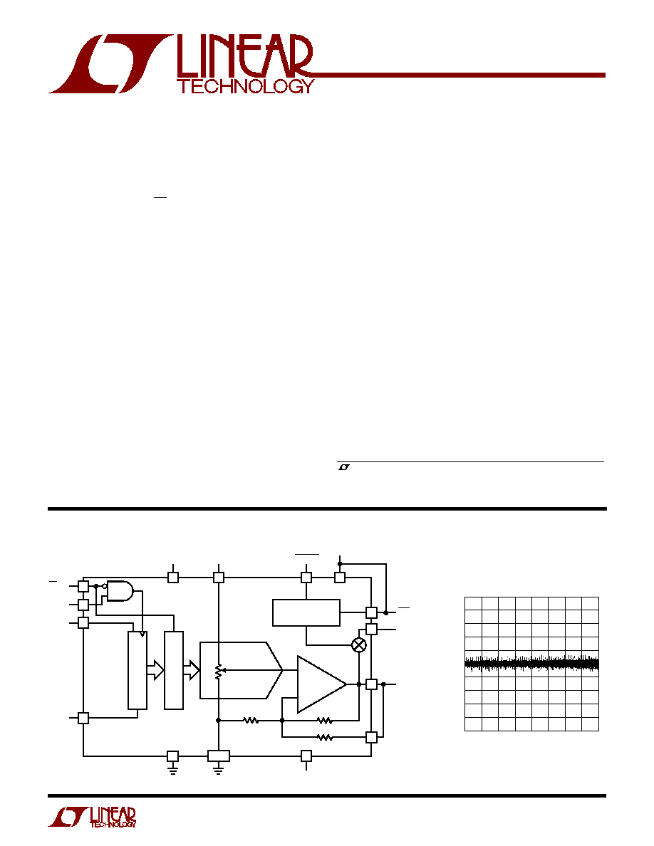
≠
+
16-BIT DAC
16-BIT DAC REGISTER
16-BIT SHIFT REGISTER
POWER-ON RESET
SUPPLY SENSE
CLR
V
RST
AV
DD
5V
RSTOUT
V
OUT
UNI/BIP
REFLO
DGND
1650 TA01
10
8
7
5
6
12,13
4.096V
5V
≠ 5V
CS/LD
CLK
D
IN
D
OUT
REFHI
11
15
9
2
1
16
4
AV
SS
14
DV
DD
3
CODE
0
≠ 1.0
DNL ERROR (LSB)
≠ 0.8
≠ 0.4
≠ 0.2
0
1.0
0.4
16384
32768
1650 TA02
≠ 0.6
0.6
0.8
0.2
49152
65535
Differential Nonlinearity
vs Input Code
s
16-Bit Monotonic Over Temperature
s
Low Glitch Impulse: 2nV-s
s
Low Noise: 30nV/
Hz
s
Buffered Rail-to-Rail Voltage Output
s
Low Power: 50mW from
±
5V Supplies
s
Unipolar or Bipolar Output (0V to V
REF
or
±
V
REF
)
s
4-Quadrant Multiplying Capability
s
Asynchronous Clear to User-Defined Voltage
s
Power-On Reset
s
Three-Wire SPI and MICROWIRE
TM
Compatible
Serial Interface
s
Schmitt Trigger On CLK Input Allows Direct
Optocoupler Interface
s
16-Pin Narrow SO Package
s
Industrial Process Control
s
Precision Industrial Equipment
s
Waveform Generation
s
Automatic Test Equipment
s
High Resolution Offset and Gain Adjustment
APPLICATIO S
U
TYPICAL APPLICATIO
U
FEATURES
DESCRIPTIO
U
, LTC and LT are registered trademarks of Linear Technology Corporation.
MICROWIRE is a trademark of National Semiconductor Corporation.
2
LTC1650
ABSOLUTE
M
AXI
M
U
M
RATINGS
W
W
W
U
ELECTRICAL CHARACTERISTICS
AV
DD
= 4.75V to 5.25V, AV
SS
= ≠ 4.75V to ≠ 5.25V, DV
DD
= 4.75V to 5.25V, REFLO = 0V, REFHI = 4.096V, V
OUT
unloaded,
T
A
= T
MIN
to T
MAX
unless otherwise noted.
(Note 1)
AV
DD
, DV
DD
to DGND .............................. ≠ 0.5V to 7.5V
TTL Input Voltage .................................... ≠ 0.5V to 7.5V
V
OUT
, V
RST
................................ ≠ 0.5V to (AV
DD
+ 0.5V)
AV
SS
.........................................................0.5V to ≠ 7.5V
Operating Temperature Range
LTC1650C............................................... 0
∞
C to 70
∞
C
LTC1650I ............................................ ≠ 40
∞
C to 85
∞
C
Maximum Junction Temperature ......................... 125
∞
C
Storage Temperature Range ................. ≠ 65
∞
C to 150
∞
C
Lead Temperature (Soldering, 10 sec)................. 300
∞
C
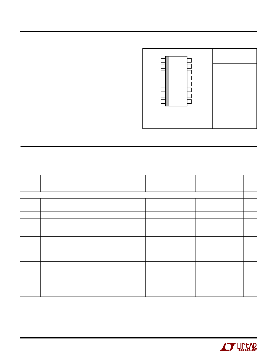
PACKAGE/ORDER I
N
FOR
M
ATIO
N
W
U
U
ORDER PART
NUMBER
TOP VIEW
S PACKAGE
16-LEAD PLASTIC SO
N PACKAGE
16-LEAD PDIP
1
2
3
4
5
6
7
8
16
15
14
13
12
11
10
9
V
OUT
V
RST
DV
DD
DGND
D
IN
D
OUT
CLK
CS/LD
UNI/BIP
AV
DD
AV
SS
REFLO S
REFLO F
REFHI
RSTOUT
CLR
T
JMAX
= 125
∞
C,
JA
= 85
∞
C/ W (N)
T
JMAX
= 125
∞
C,
JA
= 130
∞
C/ W (S)
LTC1650ACN
LTC1650AIN
LTC1650ACS
LTC1650AIS
LTC1650CN
LTC1650IN
LTC1650CS
LTC1650IS
LTC1650CS/CN
LTC1650ACS/ACN
LTC1650IS/IN
LTC1650AIS/AIN
SYMBOL
PARAMETER
CONDITIONS
MIN
TYP
MAX
MIN
TYP
MAX
UNITS
DAC Characteristics, Unipolar/Bipolar Output Unless Otherwise Noted
Resolution
q
16
16
Bits
Monotonicity
q
16
16
Bits
DNL
Differential Nonlinearity
Guaranteed Monotonic (Note 2)
q
±
0.15
±
0.9
±
0.15
±
0.5
LSB
INL
Integral Nonlinearity
Integral Nonlinearity (Note 2)
q
±
4
±
16
±
4
±
8
LSB
Bipolar Zero Error
T
A
= 25
∞
C
±
5
±
12
±
5
±
12
LSB
Bipolar Zero Error
T
A
= T
MIN
to T
MAX
q
±
18
±
18
LSB
V
OS
Unipolar Offset Error
T
A
= T
MIN
to T
MAX
q
±
0.5
±
12
±
0.5
±
12
LSB
V
OS
TC
Offset Error Temperature
±
0.5
±
0.5
µ
V/
∞
C
Coefficient
Gain Error
T
A
= T
MIN
to T
MAX
q
±
4
±
18
±
4
±
12
LSB
Gain Error Temperature
±
0.5
±
0.5
ppm/
∞
C
Coefficient
Bipolar Negative
T
A
= T
MIN
to T
MAX
q
±
1
±
16
±
1
±
12
LSB
Full-Scale Error
See Definitions Section
Bipolar Negative
See Definitions Section
±
0.75
±
0.75
ppm/
∞
C
Full-Scale Error Tempco
Consult factory for Military grade parts.
3
LTC1650
ELECTRICAL CHARACTERISTICS
AV
DD
= 4.75V to 5.25V, AV
SS
= ≠ 4.75V to ≠ 5.25V, DV
DD
= 4.75V to 5.25V, REFLO = 0V, REFHI = 4.096V, V
OUT
unloaded,
T
A
= T
MIN
to T
MAX
unless otherwise noted.
SYMBOL
PARAMETER
CONDITIONS
MIN
TYP
MAX
UNITS
Power Supply Characteristics
AV
DD
Positive Supply Voltage
q
4.75
5.0
5.25
V
DV
DD
Positive Supply Voltage
q
4.75
5.0
5.25
V
AV
SS
Negative Supply Voltage
q
≠ 4.75
≠ 5.0
≠ 5.25
V
I
AVDD
AV
DD
Supply Current
4.75V
AV
DD
5.25V (Note 5)
q
5
7.5
mA
I
AVSS
AV
SS
Supply Current
≠ 5.25V
AV
SS
≠ 4.75V (Note 5)
q
≠ 7.5
≠ 5
mA
I
DVDD
DV
DD
Supply Current
4.75V
DV
DD
5.25V (Note 5)
q
0.1
0.25
mA
PSRR
AV
DD
, DV
DD
Supply Rejection
4.75V
AV
DD
, DV
DD
5.25V
q
0.5
1.5
LSB/V
AV
SS
Supply Rejection
≠ 5.25V
AV
SS
≠ 4.75V
q
0.5
1.5
LSB/V
Reference Input
R
IN
Reference Input Resistance
q
2.5
5
7.5
k
REFHI Range
q
≠ 4.0
4.0
4.5
V
REFLO Range
q
≠ 1.0
0
1.0
V
Op Amp DC Performance
Short-Circuit Current Low
V
OUT
Shorted to GND
q
25
50
mA
Short-Circuit Current High
V
OUT
Shorted to V
CC
q
25
50
mA
Output Impedance
Measured at Midscale
0.15
DAC Output Range
Unipolar Mode (Note 9)
0V to V
REF
V
Bipolar Mode (Note 9)
±
V
REF
V
AC Performance
Voltage Output Slew Rate
q
0.8
2.0
V/
µ
s
Voltage Output Settling Time
Unloaded (Note 4)
4
µ
s
Midscale Glitch Impulse
1.8
nV-s
Digital Feedthrough
0.05
nV-s
Output Noise Voltage Density
1kHz to 100kHz (Note 6)
30
nV/
Hz
SINAD
Signal-to-Noise + Distortion Ratio
REFHI = 1kHz 4V
P-P
96
dB
4
LTC1650
ELECTRICAL CHARACTERISTICS
AV
DD
= 4.75V to 5.25V, AV
SS
= ≠ 4.75V to ≠ 5.25V, DV
DD
= 4.75V to 5.25V, REFLO = 0V, REFHI = 4.096V, V
OUT
unloaded,
T
A
= T
MIN
to T
MAX
unless otherwise noted.
Note 4: To
±
1LSB. Unipolar mode. DAC switched between all 1s and all 0s.
Note 5: Digital Inputs at 0V or DV
DD
.
Note 6: Measured at V
OUT
. REFHI = REFLO = 0V, unipolar mode.
Note 7: When part powers up or when it is reset, the output is connected
to V
RST
through this switch.
Note 8: Reset is active when any supply goes below this threshold.
Note 9: REFLO = 0V, REFHI = V
REF
. For REFLO
0V see Operation section.
The
q
denotes specifications which apply over the full operating
temperature range.
Note 1: Absolute Maximum Ratings are those values beyond which the life
of a device may be impaired.
Note 2: Nonlinearity is defined from code 0 to code 65535 (full scale)
(end point INL, see Definitions section).
Note 3: Guaranteed by design. Not subject to test.
SYMBOL
PARAMETER
CONDITIONS
MIN
TYP
MAX
UNITS
Digital I/O Characteristics
V
IH
Digital Input High Voltage
q
2.4
V
V
IL
Digital Input Low Voltage
q
0.8
V
V
OH
Digital Output High Voltage
I
OUT
= ≠1mA, D
OUT
Only
q
V
CC
≠ 1.0
V
V
OL
Digital Output Low Voltage
I
OUT
= 1mA, D
OUT
Only
q
0.4
V
I
LK
Digital Input Leakage
V
IN
= GND to V
CC
q
±
10
µ
A
C
IN
Digital Input Capacitance
(Note 3)
10
pF
Reset Characteristics
R
ON
V
OUT
and V
RST
Switch Resistance
V
RST
= 0.5V (Note 7)
q
200
500
Threshold Voltage for Reset
AV
DD
or DV
DD
(Note 8)
q
1.5
2.5
3.2
V
AV
SS
(Note 8)
q
1.5
2.5
3.2
V
Switching Characteristics
t
1
D
IN
Valid to CLK Setup
q
40
ns
t
2
D
IN
Valid to CLK Hold
q
0
ns
t
3
CLK High Time
(Note 3)
q
40
ns
t
4
CLK Low Time
(Note 3)
q
40
ns
t
5
CS/LD Pulse Width
(Note 3)
q
50
ns
t
6
LSB CLK to CS/LD
(Note 3)
q
40
ns
t
7
CS/LD Low to CLK
(Note 3)
q
20
ns
t
8
D
OUT
Output Delay
C
LOAD
= 100pF
q
5
45
150
ns
t
9
CLK Low to CS/LD Low
(Note 3)
q
20
ns
t
10
CLR Pulse Width
q
50
ns
5
LTC1650
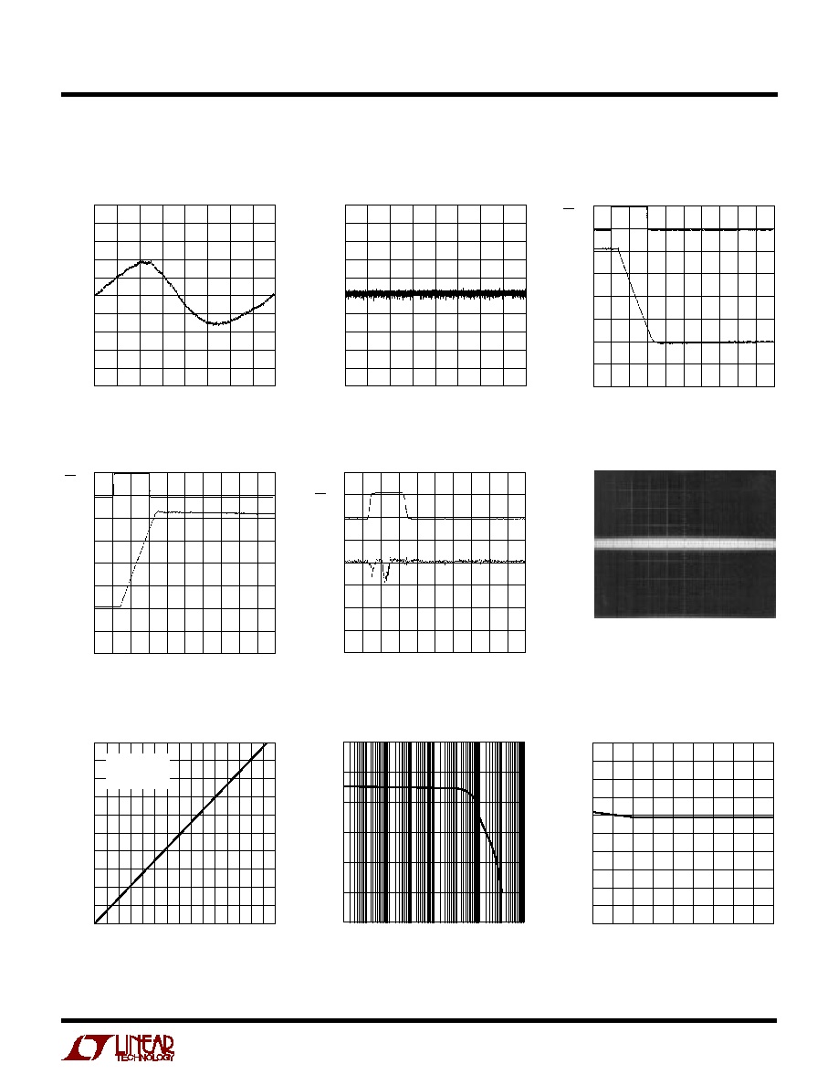
TYPICAL PERFOR A CE CHARACTERISTICS
U
W
Integral Nonlinearity (INL) vs
Input Code
CODE
0
16384
32768
49152
65535
INL ERROR (LSB)
1650 G01
5
4
3
2
1
0
≠1
≠2
≠3
≠4
≠5
1
µ
s/DIV
1650 G03
CS/LD
5V/DIV
4.096V
0V
V
OUT
1V/DIV
CODE
0
16384
32768
49152
65535
DNL ERROR (LSB)
1650 G02
1.0
0.8
0.6
0.4
0.2
0
≠0.2
≠0.4
≠0.6
≠0.8
≠1.0
Differential Nonlinearity (DNL) vs
Input Code
Large Signal Settling Time
Large Signal Settling Time
Mid-Scale Glitch
Broadband Noise
500ns/DIV
1650 G05
CS/LD
5V/DIV
V
OUT
10mV/DIV
1
µ
s/DIV
1650 G04
CS/LD
5V/DIV
V
OUT
1V/DIV
4.096V
0V
50
µ
V/DIV
REFERRED
TO DAC
OUTPUT
BW = 100kHz
200
µ
s/DIV
1650 G06
Minimum Supply Headroom for
Full Output Swing vs Load Current
Reference Feedthrough
AV
DD
Supply Current vs
Temperature
FREQUENCY (Hz)
ATTENUATION (dB)
100
90
80
70
60
50
40
1
10k
1M
100M
1650 G08
100
LOAD CURRENT (mA)
0
5.0
10.0
15.0
V
CC
≠ V
OUT
1650 G07
1.0
0.9
0.8
0.7
0.6
0.5
0.4
0.3
0.2
0.1
0
V
OUT
< 1LSB
V
OUT
= 4.096V
CODE: ALL 1's
TEMPERATURE (
∞
C)
≠55 ≠35 ≠15
5
25
45
65
85 105 125
SUPPLY CURRENT (mA)
1650 G09
5.5
5.4
5.3
5.2
5.1
5.0
4.9
4.8
4.7
4.6
4.5
6
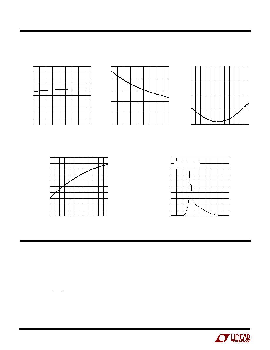
LTC1650
DV
DD
Supply Current vs
Temperature
Offset Error vs Temperature
TYPICAL PERFOR A CE CHARACTERISTICS
U
W
TEMPERATURE (
∞
C)
≠55 ≠35 ≠15
5
25
45
65
85 105 125
SUPPLY CURRENT (mA)
1650 G10
≠4.5
≠4.6
≠4.7
≠4.8
≠4.9
≠5.0
≠5.1
≠5.2
≠5.3
≠5.4
≠5.5
TEMPERATURE (
∞
C)
≠55 ≠35 ≠15
5
25
45
65
85 105 125
SUPPLY CURRENT (
µ
A)
1650 G11
25
20
15
10
5
0
TEMPERATURE (
∞
C)
OFFSET ERROR (LSB)
1650 G12
0
≠0.5
≠1.0
≠1.5
≠2.0
≠55
≠25
5
35
65
95
125
AV
SS
Supply Current vs
Temperature
Supply Current vs Logic Input
Voltage
Gain Error vs Temperature
LOGIC INPUT VOLTAGE (V)
0
1
2
3
4
5
D
VDD
SUPPLY CURRENT (mA)
1650 G14
2
1
0
ALL LOGIC INPUTS
TIED TOGETHER
TEMPERATURE (
∞
C)
≠55
≠25
5
35
65
95
125
GAIN ERROR (LSB)
1650 G13
0
≠1
≠2
≠3
≠4
≠5
≠6
≠7
≠8
≠9
≠10
PI
N
FU
N
CTIO
N
S
U
U
U
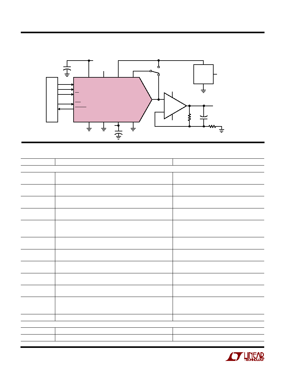
V
OUT
(Pin 1): The Rail-to-Rail Deglitched DAC Output.
The output will swing from REFLO to REFHI in unipolar
mode and from (2 ∑ REFLO ≠ REFHI) to REFHI in bipolar
mode.
V
RST
(Pin 2): The user-defined voltage to which the output
gets reset when CLR is active, when any of the supplies
drop below 2.5V or when the part powers-up. The output
will stay at this voltage until a new code is loaded into the
DAC register.
DV
DD
(Pin 3): The Digital Positive Supply Input. 4.75V
DV
DD
5.25V.
DGND (Pin 4): Digital Ground.
D
IN
(Pin 5): The TTL Level Input for the Serial Interface
Data. Data on the D
IN
pin is latched into the shift register
on the rising edge of the serial clock. Data is loaded as one
16-bit word, MSB first.
D
OUT
(Pin 6): The output of the shift register that be-
comes valid on the rising edge of the serial clock.
7
LTC1650
CLK (Pin 7): The TTL Level Input for the Serial Interface
Clock.
CS/LD (Pin 8): The TTL Level Input for the Serial Interface
Enable and Load Control. When CS/LD is low, the CLK
signal is enabled so the data can be clocked in. When
CS/LD is pulled high, data is loaded from the shift register
into the DAC register, updating the DAC output.
CLR (Pin 9): The DAC is cleared to V
RST
when this pin is
pulled low. It should be logic high for normal operation.
RSTOUT (Pin 10): The logic output pin that goes active
when any of the supplies drop below 2.5V. This pin is
active low.
REFHI (Pin 11): The Reference Input Pin. The DAC is
capable of 4-quadrant multiplying; this pin can swing
from 4.5V to ≠ 4V.
REFLO F/REFLO S (Pins 12, 13): The Force and Sense Pin
for the Lower Reference Input. This should nominally be
tied to ground. This pin can swing from ≠ 1V to 1V.
AV
SS
(Pin 14): The Analog Negative Supply Input. ≠ 5.25V
AV
SS
≠ 4.75V. Requires a bypass capacitor to ground.
AV
DD
(Pin 15): The Analog Positive Supply Input. 4.75V
AV
DD
5.25V. Requires a bypass capacitor to ground.
UNI/BIP (Pin 16): The Unipolar/Bipolar Selection Pin. For
unipolar operation, tie this pin to V
OUT
and for bipolar
operation, tie this pin the REFHI.
PI
N
FU
N
CTIO
N
S
U
U
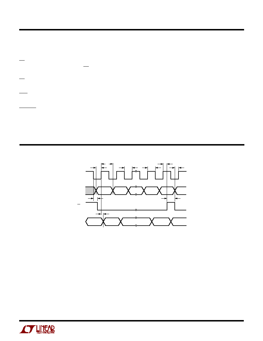
U
CLK
t
1
D
IN
CS/LD
D
OUT
B14
B15
B14
B13
B1
B0
LSB
B15
MSB
B13
B0
B1
1650 TD
(PREVIOUS
WORD)
t
9
t
8
t
6
t
7
t
4
t
3
t
5
t
2
TI I G DIAGRA
U
W
W

8
LTC1650
DEFI
N
ITIO
N
S
U
U
Resolution (n)
Resolution is defined as the number of digital input bits,
n. It defines the number of DAC output states (2
n
) that
divide the full-scale range. The resolution does not imply
linearity.
Full-Scale Voltage (V
FS
)
This is the output of the DAC when all bits are set to 1. The
output will swing from REFLO to REFHI in unipolar mode
and from (2 ∑ REFLO ≠ REFHI) to REFHI when in bipolar
mode.
Voltage Offset Error (V
OS
)
This is the voltage at the output when the DAC is loaded
with all zeros.
Least Significant Bit (LSB)
One LSB is the ideal voltage difference between two
successive codes.
LSB = (V
FS
≠ V
OS
)/(2
n
≠ 1) = (V
FS
≠ V
OS
)/65535
Integral Nonlinearity (INL)
Endpoint INL is the maximum deviation from a straight
line passing through the endpoints of the DAC transfer
curve. It is measured after adjusting out gain and offset
error for the DAC.
Differential Nonlinearity (DNL)
DNL is the difference between the measured change and
the ideal 1LSB change between any two adjacent codes.
The DNL error between any two codes is calculated as
follows:
DNL = (
V
OUT
≠ LSB)/LSB
V
OUT
= The measured voltage difference between two
adjacent codes.
Gain Error (GE)
Gain error is the difference between the full-scale output of
a DAC from its ideal full-scale value after offset error has
been adjusted for.
Bipolar Zero Error
When configured for bipolar output and with REFLO tied
to 0V, the LTC1650 output should be 0V with (100...00)
loaded in. Any deviation from 0V at this code is called
bipolar zero error.
Bipolar Negative Full-Scale Error
This is the offset error of the LTC1650 in bipolar mode.

9
LTC1650
OPERATIO
U
Serial Interface
The data on the D
IN
input is loaded into the shift register
on the rising edge of the clock. Data is loaded as one
16-bit word, MSB first. The DAC register loads the data
from the shift register when CS/LD is pulled high. The
clock is disabled internally when CS/LD is high. Note: CLK
must be low before CS/LD is pulled low to avoid an extra
internal clock pulse.
The buffered output of the 16-bit shift register is available
on the D
OUT
pin which swings from DGND to DV
DD
.
Multiple LTC1650s may be daisy-chained together by
connecting the D
OUT
pin to the D
IN
pin of the next chip
while the clock and CS/LD signals remain common to all
chips in the daisy chain. The serial data is clocked to all of
the chips, then the CS/LD signal is pulled high to update all
of them simultaneously.
When CLR is pulled low or when the part powers up, the
output connects through an internal pass gate to V
RST
and
will go to whatever voltage is on V
RST
. When any of three
supplies (DV
DD
, AV
DD
, |AV
SS
|) goes below 2.5V, the
RSTOUT pin goes low and stays low as long as the supply
is below 2.5V. The power-on reset is also activated when
one of the supplies drops below 2.5V and the output is
then connected to V
RST
. The output connects to V
RST
when any of three conditions occur: CLR goes low, the part
powers up or one of the supplies drops below 2.5V. This
condition exists as long as CS/LD is low. As soon as CS/
LD goes high, the DAC register is loaded with the data in
the shift register and the output will settle to its new value.
Voltage Output
The LTC1650 rail-to-rail buffered output can source or
sink 5mA over the entire operating temperature range. The
output can swing to within a few millivolts of either supply
rail when unloaded and has an equivalent output resis-
tance of 50
when driving a load to the rails. The buffer
amplifier can drive 1000pF without going into oscillation.
The LTC1650 has a deglitched voltage output. The midscale
glitch is less than 2nV-s. The digital feedthrough is about
0.05nV-s.
Output Ranges
The LTC1650 is capable of unipolar or bipolar output
swing. When the UNI/BIP pin is connected to V
OUT
the part
is configured for unipolar operation and the output will
swing from REFLO to REFHI. When UNI/BIP is connected
to REFHI the part is configured in bipolar mode and the
output will swing from (2 ∑ REFLO ≠ REFHI) to REFHI and
will be at REFLO at midscale. With REFLO = 0V the output
swing is
±
REFHI in bipolar mode and 0V to REFHI in
unipolar mode.
10
LTC1650
TYPICAL APPLICATIO
U
16-Bit Industrial Process Controller
5V
0.1
µ
F
+
µ
P
CONTROL VOLTAGE
0V TO 4.5V
(69
µ
V/LSB)
5V
5V
CLK
D
IN
CS/LD
CLR
RSTOUT
D
OUT
V
OUT
1650 TA03
LTC1650
REFHI
AV
DD
DV
DD
UNI/BIP
REFLO F/S
DGND
AV
SS
V
RST
IN
LT1019-4.5
4.5V
7.5V
0.1
µ
F
+
11
LTC1650
PACKAGE DESCRIPTIO
N
U
Dimensions in inches (millimeters) unless otherwise noted.
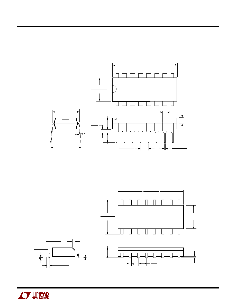
N Package
16-Lead PDIP (Narrow 0.300)
(LTC DWG # 05-08-1510)
N16 1197
0.255
±
0.015*
(6.477
±
0.381)
0.770*
(19.558)
MAX
16
1
2
3
4
5
6
7
8
9
10
11
12
13
14
15
0.020
(0.508)
MIN
0.125
(3.175)
MIN
0.130
±
0.005
(3.302
±
0.127)
0.065
(1.651)
TYP
0.045 ≠ 0.065
(1.143 ≠ 1.651)
0.018
±
0.003
(0.457
±
0.076)
0.100
±
0.010
(2.540
±
0.254)
0.009 ≠ 0.015
(0.229 ≠ 0.381)
0.300 ≠ 0.325
(7.620 ≠ 8.255)
0.325
+0.035
≠0.015
+0.889
≠0.381
8.255
(
)
*THESE DIMENSIONS DO NOT INCLUDE MOLD FLASH OR PROTRUSIONS.
MOLD FLASH OR PROTRUSIONS SHALL NOT EXCEED 0.010 INCH (0.254mm)
0.016 ≠ 0.050
0.406 ≠ 1.270
0.010 ≠ 0.020
(0.254 ≠ 0.508)
◊
45
∞
0
∞
≠ 8
∞
TYP
0.008 ≠ 0.010
(0.203 ≠ 0.254)
1
2
3
4
5
6
7
8
0.150 ≠ 0.157**
(3.810 ≠ 3.988)
16
15
14
13
0.386 ≠ 0.394*
(9.804 ≠ 10.008)
0.228 ≠ 0.244
(5.791 ≠ 6.197)
12
11
10
9
S16 0695
0.053 ≠ 0.069
(1.346 ≠ 1.752)
0.014 ≠ 0.019
(0.355 ≠ 0.483)
0.004 ≠ 0.010
(0.101 ≠ 0.254)
0.050
(1.270)
TYP
DIMENSION DOES NOT INCLUDE MOLD FLASH. MOLD FLASH
SHALL NOT EXCEED 0.006" (0.152mm) PER SIDE
DIMENSION DOES NOT INCLUDE INTERLEAD FLASH. INTERLEAD
FLASH SHALL NOT EXCEED 0.010" (0.254mm) PER SIDE
*
**
S Package
16-Lead Plastic Small Outline (Narrow 0.150)
(LTC DWG # 05-08-1610)
Information furnished by Linear Technology Corporation is believed to be accurate and reliable.
However, no responsibility is assumed for its use. Linear Technology Corporation makes no represen-
tation that the interconnection of its circuits as described herein will not infringe on existing patent rights.
12
LTC1650
©
LINEAR TECHNOLOGY CORPORATION 1998
1650f LT/TP 0199 4K ∑ PRINTED IN USA
Linear Technology Corporation
1630 McCarthy Blvd., Milpitas, CA 95035-7417
(408) 432-1900
q
FAX: (408) 434-0507
q
www.linear-tech.com
RELATED PARTS
TYPICAL APPLICATIO
U
A
±
10V Bipolar Output 16-Bit DAC
≠5V
0.1
µ
F
+
µ
P
0V TO 10V
(UNIPOLAR MODE)
≠10V TO 10V
(BIPOLAR MODE)
BIPOLAR
UNIPOLAR
5V
5V
15V
≠15V
CLK
D
IN
CS/LD
CLR
RSTOUT
V
OUT
1650 TA04
LTC1650
REFHI
AV
DD
DV
DD
UNI/BIP
REFLO
DGND
AV
SS
V
RST
IN
OUT
IN
LT1019-4.5
15V
0.1
µ
F
+
≠
+
LT1468
110k
90k
+
10pF
PART NUMBER
DESCRIPTION
COMMENTS
DACs
LTC1257
Single 12-Bit V
OUT
DAC, Full Scale: 2.048V, V
CC
: 4.75V to 15.75V,
5V to 15V Single Supply, Complete V
OUT
DAC in
Reference Can Be Overdriven Up to 12V, i.e., FS
MAX
= 12V
SO-8 Package
LTC1446/LTC1446L
Dual 12-Bit V
OUT
DACs in SO-8 Package
LTC1446: V
CC
= 4.5V to 5.5V, V
OUT
= 0V to 4.095V
LTC1446L: V
CC
= 2.7V to 5.5V, V
OUT
= 0V to 2.5V
LTC1448
Dual 12-Bit V
OUT
DAC, V
CC
: 2.7V to 5.5V
Output Swings from GND to REF. REF Input
Can Be Tied to V
CC
LTC1450/LTC1450L
Single 12-Bit V
OUT
DACs with Parallel Interface
LTC1450: V
CC
= 4.5V to 5.5V, V
OUT
= 0V to 4.095V
LTC1450L: V
CC
= 2.7V to 5.5V, V
OUT
= 0V to 2.5V
LTC1451/LTC1452/
Single 12-Bit V
OUT
DACs with Serial Interface
LTC1451: V
CC
= 4.5V to 5.5V, V
OUT
= 0V to 4.095V
LTC1453
LTC1452: V
CC
= 2.7V to 5.5V, V
OUT
= 0V to 2 ∑ V
REF
LTC1453: V
CC
= 2.7V to 5.5V, V
OUT
= 0V to 2.5V
LTC1454/LTC1454L
Dual 12-Bit V
OUT
DACs in SO-16 Package with Added Functionality
LTC1454: V
CC
= 4.5V to 5.5V, V
OUT
= 0V to 4.095V
LTC1454L: V
CC
= 2.7V to 5.5V, V
OUT
= 0V to 2.5V
LTC1456
Single Rail-to-Rail Output 12-Bit DAC with Clear Pin,
Low Power, Complete V
OUT
DAC in SO-8
Full Scale: 4.095V, V
CC
: 4.5V to 5.5V
Package with Clear Pin
LTC1458/LTC1458L
Quad 12 Bit Rail-to-Rail Output DACs with Added Functionality
LTC1458: V
CC
= 4.5V to 5.5V, V
OUT
= 0V to 4.095V
LTC1458L: V
CC
= 2.7V to 5.5V, V
OUT
= 0V to 2.5V
LTC1595
16-Bit Serial I/O Multiplying I
OUT
DAC in SO-8
±
1LSB Max INL/DNL, Low Glitch, DAC8043
is a Pin Compatible 12-Bit DAC
LTC1596
16-Bit Serial I/O Multiplying I
OUT
DAC with Clear Pin
±
1LSB Max INL/DNL, Low Glitch, AD7543/DAC8143
are Pin Compatible 12-Bit DACs
LTC1659
Single Rail-to-Rail 12-Bit V
OUT
DAC in MSOP-8 Package,
Low Power Multiplying V
OUT
DAC in MSOP-8 Package.
V
CC
: 2.7V TO 5.5V
Output Swings from GND to REF. REF Input Can be Tied
to V
CC
LTC8043
Serial I/O Multiplying I
OUT
12-Bit DAC
8-Pin SO and PDIP
References
LT1019
Precision Voltage Reference
Ultralow Drift 5ppm/
∞
C, Initial Accuracy: 0.05%
LT1634
Micropower Precision Reference
Low Drift 10ppm/
∞
C, Initial Accuracy: 0.05%